
A low viscosity, low boiling point, clean solvent system for the rapid crystallisation of highly specular perovskite films†
Nakita K.
Noel
 a,
Severin N.
Habisreutinger
a,
Bernard
Wenger
a,
Matthew T.
Klug
a,
Maximilian T.
Hörantner
a,
Michael B.
Johnston
a,
Robin J.
Nicholas
a,
David T.
Moore
*ab and
Henry J.
Snaith
*a
a,
Severin N.
Habisreutinger
a,
Bernard
Wenger
a,
Matthew T.
Klug
a,
Maximilian T.
Hörantner
a,
Michael B.
Johnston
a,
Robin J.
Nicholas
a,
David T.
Moore
*ab and
Henry J.
Snaith
*a
aClarendon Laboratory, Department of Physics, University of Oxford, Parks Road, Oxford, OX1 3PU, UK. E-mail: h.snaith1@physics.ox.ac.uk; david.moore@nrel.gov
bNational Renewable Energy Laboratory, 15013 Denver West Parkway, Golden, USA
First published on 26th September 2016
Abstract
Perovskite-based photovoltaics have, in recent years, become poised to revolutionise the solar industry. While there have been many approaches taken to the deposition of this material, one-step spin-coating remains the simplest and most widely used method in research laboratories. Although spin-coating is not recognised as the ideal manufacturing methodology, it represents a starting point from which more scalable deposition methods, such as slot-dye coating or ink-jet printing can be developed. Here, we introduce a new, low-boiling point, low viscosity solvent system that enables rapid, room temperature crystallisation of methylammonium lead triiodide perovskite films, without the use of strongly coordinating aprotic solvents. Through the use of this solvent, we produce dense, pinhole free films with uniform coverage, high specularity, and enhanced optoelectronic properties. We fabricate devices and achieve stabilised power conversion efficiencies of over 18% for films which have been annealed at 100 °C, and over 17% for films which have been dried under vacuum and have undergone no thermal processing. This deposition technique allows uniform coating on substrate areas of up to 125 cm2, showing tremendous promise for the fabrication of large area, high efficiency, solution processed devices, and represents a critical step towards industrial upscaling and large area printing of perovskite solar cells.
Broader contextRecently, perovskite-based solar cells have raced to the front of emerging photovoltaics, competing on efficiency against well-established solar technologies. One unique selling point for perovskites is the promise of low cost manufacturing via solution processing methodologies. One hurdle could prevent large scale production of this technology is the need to move away from employing toxic, highly coordinating, high boiling point solvents. With the currently employed solvent set (primarily dimethylformamide, dimethylsulfoxide and γ-butyrolactone), it is extremely difficult to formulate inks capable of processing uniform films over large areas, and subsequently, fully remove the solvents. Hence, a largely unexplored challenge is to find a more suitable solvent set for manufacturing perovskite solar cells. Here, we demonstrate the use of a low-viscosity, low boiling point solvent system for the deposition of perovskite films. Using a combination of methylamine and acetonitrile, we have formulated a solvent which completely dissolves the precursors of the CH3NH3PbI3 perovskite, resulting in rapid, room temperature crystallisation of highly specular films with enhanced carrier lifetimes as compared to their DMF based counterparts. Using this solvent, we demonstrate one step spin-coating which is able to deposit uniform, pinhole-free perovskite films on substrates as large as 125 cm2, and fabricate solar cells achieving stabilised efficiencies of over 18%. The reduction of viscosity, boiling point and toxicity of this solvent, coupled with the new ability to easily coat larger area substrates with little to no decrease in the film quality, overcomes a previous challenge for the commercialisation of printable perovskite photovoltaics. |
Introduction
When metal halide perovskites were first applied as light absorbing nanoparticles in solar cells by Miyasaka and co-workers in 2009, the solar light to electrical power conversion efficiency stood at 3%.1 However, the field took off in 2012 when reports were made of photovoltaic devices achieving power conversion efficiencies of 9.2% employing a mesoporous TiO2 layer,2 and 10.9% employing an Al2O3 scaffold.3 The latter showed that perovskites are not only efficient absorbers, but that they are capable of sustaining long range charge transport in thin films,4 and function well in simple thin-film planar heterojunctions.5 Since then, there has been burgeoning research into the field of perovskite photovoltaics, with perovskites being heralded as a “wonder material” that holds the promise to completely transform the energy landscape.6 From its humble beginnings, perovskite-based photovoltaics are now leading the pack of emerging solar technologies, already competing with inorganic thin-film solar cells and mainstream multi-crystalline silicon, with certified efficiencies of 22.1%,7 a feat which, remarkably, has been achieved in under 4 years since the first reports in 2012. Additionally, another extremely desirable feature of perovskite photovoltaics is that this technology possesses a far lower energy payback time than its crystalline silicon counterpart.8Apart from the obvious lure of high power conversion efficiencies, one of the most attractive features of perovskites is the simplicity with which high-quality films of this material can be fabricated. While perovskite films have been deposited through a variety of different methods,5,9–12 in a laboratory setting, one-step spin coating remains the simplest and quickest route to the formation of high quality perovskite layers. It must be noted however, that in the initial work done on thin solid films of CH3NH3PbI3, the biggest challenges were poor film morphology and inadequate surface coverage. Perovskite films formed from a DMF-based solution of methylammonium iodide (MAI) and PbI2 precursor salts were often quite rough with a large number of pinholes.4,13 In an effort to improve film morphology, different variations of this method have been developed, such as the utilisation of solvent mixtures,14 a variety of lead salt precursors,15–17 as well as the addition of a solvent quenching step.18 Most recently, a popular approach involves the inclusion of dimethyl sulfoxide (DMSO) in the precursor solution, whether through the simple addition of the solvent to the conventional DMF-based precursor solution,19–21 or via the use of a pre-synthesised PbI2(DMSO)2 complex.22,23 These methods have been shown to vastly improve film quality, allowing for the formation of much smoother films with greatly increased surface coverage.
To date, all reports of highly efficient perovskite solar cells, in which the perovskite layer is fabricated via solution techniques use or incorporate high boiling point, polar, aprotic solvents. While the most frequently used solvent is N,N-dimethylformamide (DMF),3,24–26 other solvents include dimethyl sulfoxide (DMSO),21 γ-butyrolactone (GBL) and dimethylacetamide (DMA),27 and mixtures thereof. The choice of solvent is limited by the lead halide salts, which are either sparingly or completely insoluble in most of the solvents commonly used in large scale deposition techniques. Solvent handling issues and toxicology concerns associated with a factory operating with highly coordinating, toxic solvents such as DMF, represent a major barrier to large scale manufacturing.28 As such, the substitution of these solvents is required to enable progression of the industrial upscaling of printable perovskite solar cells.29,30 Beyond these practical considerations, one of the disadvantages to using high boiling point solvents such as these, is the need to heat films (≥100 °C) for a prolonged period of time after deposition in order to drive off the excess solvent and to induce crystallisation of the perovskite films. This can be somewhat circumvented by the use of solvent quenching, where a film is drenched with an anti-solvent at a specified time during spin-coating, resulting in the immediate crystallisation of the perovskite material,18–20,31,32 or by applying a vacuum on the sample right after spin-coating.33 We note that while both these methods have been shown to produce smooth, pinhole free films, the addition of the quenching and vacuum steps are likely to reduce the ease with which the technique can be transferred from lab scale to large scale deposition techniques, especially roll-to-roll printing.
Another post-fabrication strategy to improve the film quality involves the use of methylamine (MA) gas to “heal” defects in crystalline perovskite films. This has previously been reported by Zhou et al.34 where, upon exposure to the methylamine, crystals of the methylammonium lead iodide (CH3NH3PbI3) were seen to “melt” and subsequently reform after the removal of the gas. This “healing” process served to significantly reduce the surface roughness of the perovskite films and form dense, pinhole free layers.
Herein, we propose an alternative strategy employing methylamine. We postulate that by introducing MA into an appropriate low boiling point, low viscosity solvent, we can increase the solvating power of that solvent with respect to the perovskite precursor salts. Through this method, we could combine the benefits of the methylamine treatment with the convenience of solution processing, giving us a precursor solution which would yield high quality films with a smaller defect density. This approach could open a myriad of different possibilities, such as the ability to use lower boiling point solvents to facilitate the rapid crystallisation of perovskite films.
Acetonitrile (ACN) is a low boiling point, highly polar, aprotic solvent which is very often employed in non-aqueous ink formulations and as such is a prime candidate for the solvation of the perovskite precursor salts. However, while methylammonium iodide (CH3NH3I) can be dissolved in neat ACN, PbI2 is completely insoluble in ACN, precluding its use as a solvent for perovskite materials. In the study presented here, we use methylamine to enhance the solvating power of acetonitrile. We show that the composite ACN/MA solvent system can be used for the dissolution of the CH3NH3PbI3 precursor salts. Upon spin-coating this precursor solution, we obtain extremely smooth, pinhole-free films of CH3NH3PbI3 which crystallise at room temperature. We present a spectroscopic and device based investigation and show that the films processed from the ACN/MA compound solvent exhibit long carrier lifetimes, allowing the corresponding planar heterojunction devices to achieve JV scanned efficiencies of up to 19% and stabilised efficiencies of over 18%. Additionally, we demonstrate larger 0.7 cm2 cells at over 15% efficiency and produce evenly coated, highly specular and uniform perovskite films on substrate sizes ranging from 1.44 cm2 to 125 cm2 without sacrificing film quality.
Results and discussion
To saturate the ACN with MA, we bubble MA gas into the ACN. We describe the details of solvent preparation, as well as the physical properties of the solvent in the ESI.† Before the MA is dissolved in the ACN, the perovskite precursor salts form a black precipitate of CH3NH3PbI3, which dissolves upon the addition of methylamine to give a pale yellow solution. We show photographs of the dispersion and corresponding solution in Fig. 1a. We illustrate the impact of using different carrier solvents in this way by comparing ACN against water and ethanol. Despite the presence of MA, we obtain either a milky white or yellow dispersion in both water and ethanol. We show photographs of these solutions in Fig. S2 (ESI†). This suggests that while the dissolution of the precursor salts is carried out by the MA, the choice of carrier solvent is of great importance. Like both DMF and DMSO, ACN is a polar, aprotic solvent; whereas both water and ethanol are protic solvents. Empirically, we postulate that the polar, aprotic nature is an important property of the solvent. We note that in this solvent system, the ACN primarily acts as a conduit for the methylamine gas. The dissolution of the perovskite precursors is carried out by the methylamine gas itself. In this case, we propose an interaction similar to that proposed by Zhou et al., where the methylamine serves to “melt” the perovskite material through the formation of a liquid perovskite phase (CH3NH3PbI3·xCH3NH2), which is miscible within the ACN, but which subsequently solidifies upon the evaporation of the ACN/MA solvent. | ||
Fig. 1 (a) Vials of perovskite precursors CH3NH3 I![[thin space (1/6-em)]](https://www.rsc.org/images/entities/char_2009.gif) :PbI2 (1:1.06 molar ratio) in neat ACN, and in the ACN/MA solvent mixture. (b) X-Ray diffractograms of a film of CH3NH3PbI3 spin coated from a precursor solution where ACN/MA is the solvent, measured at different annealing time intervals (Tanneal = 100 °C). :PbI2 (1:1.06 molar ratio) in neat ACN, and in the ACN/MA solvent mixture. (b) X-Ray diffractograms of a film of CH3NH3PbI3 spin coated from a precursor solution where ACN/MA is the solvent, measured at different annealing time intervals (Tanneal = 100 °C). | ||
With the knowledge that MA is able to dissolve perovskite salts, it follows then that other alkylamines should be able to perform a similar function. To test this theory, we used propylamine, butylamine and pentylamine to dissolve the perovskite precursor salts in combination with acetonitrile. However, while these amines do result in dissolution of the precursor material, upon spin-coating, they do not form films of neat CH3NH3PbI3 but appear to be compounds incorporating some fraction of the larger organic amines (see Fig. S3, ESI†).
Using the solution produced with the ACN/MA compound solvent, we proceeded to fabricate films of CH3NH3PbI3 for X-ray diffraction and optical characterisation. Acetonitrile is a solvent which has a boiling point of 82 °C and a vapour pressure of 9.71 kPa at standard room temperature and pressure (STP), whereas methylamine is a gas. In the case of the mixed solvent, where methylamine is dissolved in acetonitrile, we find that it has a boiling point of 80 °C and a viscosity of 0.25 cP. When depositing films of CH3NH3PbI3 from the ACN/MA compound solvent, the films appear to completely crystallise during spin-coating, showing the strong dark colour which is characteristic of polycrystalline CH3NH3PbI3. In Fig. 1b we show the X-ray diffractograms from a single representative film as spin-coated, and after annealing at 100 °C for different time intervals, alongside corresponding photographs of the film. From these diffraction patterns, we can confirm that even before annealing, the perovskite film is already formed, exhibiting the characteristic peaks of a tetragonal perovskite crystal structure. After annealing the film for 15 minutes at 100 °C, we observe the appearance of a small peak at 12.6°, which we assign to the presence of lead iodide.15 The appearance of this peak suggests the onset of “over-annealing” of the film, which is characterised by driving off some of the organic components; at the same time there is also a distinct sharpening of the characteristic perovskite peaks. The decrease in these peak widths suggests that with annealing there is either an increase in crystallinity, or grain coarsening in the films. We present the UV-Vis absorption and photoluminescence decays of the films at 0 min ≤ tanneal ≤ 60 min in Fig. S4 and S5 (ESI†).
We show the absorption and steady-state photoluminescence spectra of these films in Fig. 2. We observe the characteristic absorption onset at approximately 770 nm and steady-state photoluminescence (PL) peak at 780 nm. In Fig. 2b we show the time-resolved photoluminescence decays of a film of CH3NH3PbI3 processed from the ACN/MA mixed solvent, alongside that of films of CH3NH3PbI3−xClx and CH3NH3PbI3 fabricated from precursor solutions in DMF. We note that the CH3NH3PbI3 films are fabricated from a stoichiometric solution of MAI:PbI2, while the CH3NH3PbI3−xClx film is fabricated from a 3:1 molar ratio of MAI:PbCl2. The PL decay is influenced by a multitude of factors, including the radiative and non-radiative decay constants and the optoelectronic homogeneity of the polycrystalline films. As a general indication, the longer the PL lifetime, the slower the non-radiative decay and hence the longer lived the charge carriers and the longer the charge carrier diffusion length. We show the absorption and steady-state photoluminescence spectra of these films in Fig. 2. To quantify the photoluminescence lifetime, we fit the data with a stretched exponential function. The use of this model has been previously suggested to take into account a distribution of monomolecular recombination rates which has been observed in spatially-resolved PL studies.4,35 Although this does not explicitly consider bimolecular recombination, it provides a convenient way to compare the different films with previously published results. For the CH3NH3PbI3 film processed from the ACN/MA solvent, the average lifetime 〈τ〉 is 676 ns, much longer than that of the DMF processed films, which give 〈τ〉 values of 258 ns and 28 ns for CH3NH3PbI3−xClx and CH3NH3PbI3 respectively. This is indicative of a significant improvement of the optoelectronic quality of the films obtained through processing with this new solvent system. This result is consistent with previous results which have shown that methylamine “healing” improves the overall film quality of methylammonium based perovskite materials.34 We note however, that as a result of keeping the deposition parameters for all solutions the same, we obtain stark differences in the quality of films deposited from these different precursor solutions (see Fig. S6, ESI†).
 | ||
| Fig. 2 (a) Absorption and steady-state photoluminescence spectra of a film of MAPbI3 as spin coated from ACN/MA. (b) Time-resolved photoluminescence of films of CH3NH3PbI3 spin coated from an ACN/MA, CH3NH3PbI3−xClx spin coated from a DMF solution, and CH3NH3PbI3 spin coated from a DMF solution. The initial carrier density after pulsed excitation at 505 nm is 1016 cm−3. The solid lines are fits to a stretched exponential function. | ||
We also investigated the surface morphology of the films using scanning electron microscopy (SEM) and atomic force microscopy (AFM), and present these images in Fig. 3. As we show in Fig. 3a the crystal grains are densely packed with the sizes of individual domains ranging from between 500 nm and 700 nm. At lower magnification, the absence of pinholes in the film becomes more notable (Fig. S7, ESI†). Using AFM to estimate the surface roughness of the film we obtained a root mean square (rms) value of 7.8 nm (5 × 5 micron scan area, contact mode), a value which is comparable to the roughness which has previously been reported for this material in both films processed from a lead acetate precursor,15 and films deposited via vacuum based thermal evaporation.36 This rms value is also considerably smaller than those previously reported for films of CH3NH3PbI3 (52.2 nm) and CH3NH3PbI3−xClx (62.4 nm) processed from lead halide precursors in DMF.15 We have also fabricated a CH3NH3PbI3 film using the typically used DMF/DMSO mixture as a solvent for the precursors and obtained an rms value of 26.3 nm. Even through this method, which typically produces smooth, pinhole-free films, the surface roughness is three times higher than for those processed from the ACN/MA solvent mixture (see Fig. S8, ESI†). This effectively accounts for one of the most visually striking features of films processed from this solvent; their smooth, mirror-like appearance.
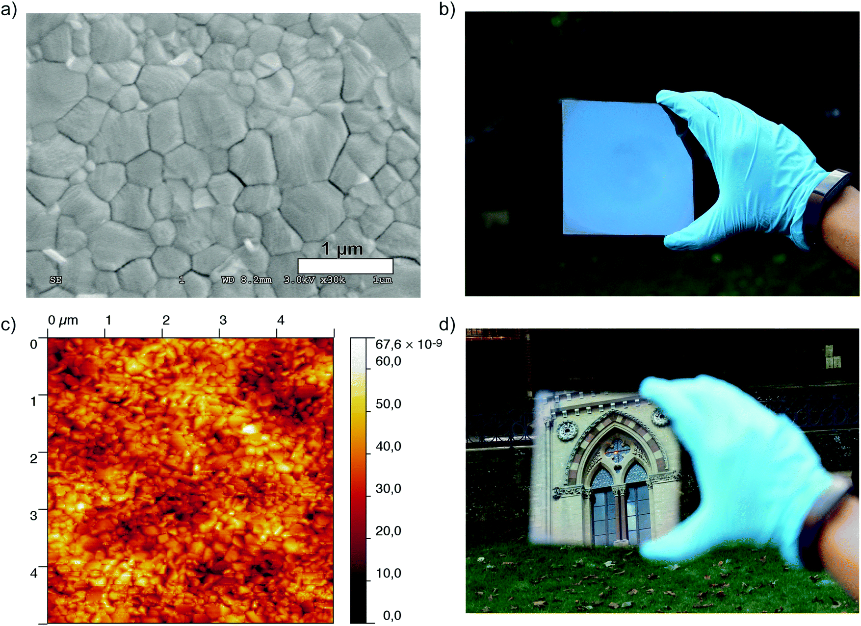 | ||
| Fig. 3 (a) Top-view SEM image of a crystalline film of CH3NH3PbI3 processed from an ACN/MA based solution. (c) A 5 μm × 5 μm AFM image of the film shown in (a). (b) and (d) Photographs of an 125 cm2, highly specular, pinhole free film of CH3NH3PbI3 deposited via spin coating from the ACN/MA solvent system. | ||
One of the added advantages of processing perovskite films from the ACN/MA solution is the ability to coat relatively large areas uniformly. In order to illustrate this, we coated a Si wafer (4 inch diameter) and investigated the film using spectral reflectance measurements. We probed the thickness at various points over the entire area and found that the perovskite layer was highly uniform, with a thickness of 329.6 ± 6.3 nm. We give the details of the measurement in the ESI† and a summary of the results obtained is presented in Fig. S9.
Having shown that through the manipulation of the solvent we can not only form incredibly smooth and pinhole-free films, but also increase the charge-carrier lifetimes, we proceed to integrate these films into photovoltaic devices. The optimal device fabrication procedure was determined by preparing a series of devices with increasing annealing times. We present the performance of these devices in Fig. S10 (ESI†). From this experiment, we determined the optimal annealing time to be 60 min. For these devices, the device stack which was used was FTO/TiO2/C60/CH3NH3PbI3/spiro-OMeTAD/Au. We show a cross-sectional SEM image of a typical device in Fig. S11 (ESI†). Consistent with previous reports on planar perovskite solar cells, we observe some hysteresis in the current–voltage curves of our devices.37 While the use of C60 has previously been shown to reduce hysteresis in the JV curves,38 we note that hysteresis is still present in these devices. A recent paper published by Yang et al. reported the elimination of hysteresis in planar CH3NH3PbI3 devices through the use of an ionic liquid, 1-butyl-3-methylimidazolium tetrafluoroborate, to modify the TiO2 compact layer.39 Through the use of this ionic liquid, while we have not been able to completely eliminate the hysteresis phenomenon, it has been greatly reduced, allowing us to achieve scanned device efficiencies of up to 19.0%, with a maximum stabilised efficiency of 18.2%. Utilising this precursor solution, we have also fabricated inverted, p–i–n, cells following the method of Wang et al.40 which deliver a maximum JV determined efficiency of 16.8% and a stabilised efficiency of 16.3%. We show the current–density voltage (JV) characteristics and steady-state efficiency of the best performing devices in Fig. 4. All devices shown in Fig. 4 have an active area of 0.09 cm2. We have also fabricated devices with larger active areas (0.7 cm2), and attained a maximum stabilised power conversion efficiency of over 15% for the p–i–n cell configuration. We show the JV curves and stabilised efficiencies for the larger area cells in the ESI† (Fig. S12–S14), and present the performance parameters in Table 1. We show the external quantum efficiency (EQE) of the champion annealed device in Fig. S15 (ESI†). By integrating the EQE over the AM 1.5 spectrum we obtain a JSC of 20.8 mA cm−2 for this device, a value which is within 5% of the JSC extracted from the solar simulator. In order to assess the diode quality of these devices we fit the JV curves to the diode equation and extracted shunt resistances of 2029 Ω cm2 and 7535 Ω cm2 for the small area n–i–p and p–i–n devices, respectively. For the larger area devices, shunt resistance values of 1862 Ω cm2 and 1189 Ω cm2 were obtained. These relatively high shunt resistances are further indication of the presence of little to no pinholes in the perovskite layer.
 | ||
| Fig. 4 Current–voltage characteristics. (a) Current–voltage characteristics of the champion ACN/MA device where the active layer annealed and 100 °C for 60 min and (c) the champion ACN/MA device in which the active layer was “degassed” under vacuum overnight. (e) Current–voltage characteristics of the champion inverted ACN/MA device where the active layer annealed and 100 °C for 60 min and (b), (d) and (f) stabilised photocurrents and efficiencies of the devices presented in (a), (c) and (e) respectively, measured by holding the devices at their JV determined maximum power point for 50 seconds. Performance parameters of each of these devices are given in Table 1. | ||
| Cell type | J sc (mA cm−2) | V oc (V) | F.F. | η (%) | η MPP | |
|---|---|---|---|---|---|---|
| Annealed (0.09 cm2) | Average | 22.4 ± 0.36 | 1.08 ± 0.02 | 0.74 ± 0.03 | 17.8 ± 0.1 | |
| Champion | 22.2 | 1.10 | 0.77 | 19.0 | 18.2 | |
| Unannealed (0.09 cm2) | Average | 22.4 ± 0.7 | 1.07 ± 0.02 | 0.66 ± 0.04 | 15.7 ± 1.3 | |
| Champion | 22.5 | 1.07 | 0.75 | 18.1 | 17.2 | |
| Inverted (0.09 cm2) | Average | 18.8 ± 0.7 | 1.10 ± 0.01 | 0.77 ± 0.03 | 16.0 ± 0.5 | |
| Champion | 19.2 | 1.10 | 0.80 | 16.8 | 16.3 | |
| Annealed (0.7 cm2) | Champion | 19.2 | 1.03 | 0.69 | 14.5 | 12.4 |
| Inverted (0.7 cm2) | Champion | 20.3 | 1.10 | 0.70 | 15.3 | 15.0 |
The annealing process can play several roles in perovskite thin films; beyond simply crystallising the material, heat treatments can serve to remove residual solvent, change grain structure, and result in advantageous changes to the overall film stoichiometry. It is interesting to note that although we do not observe an extremely significant change in the diffraction pattern of the material after 15 minutes of annealing (shown in Fig. 2), the power conversion efficiency of these devices is significantly enhanced with even a short annealing time. There could be multiple reasons for this: firstly, there may be residual solvent still present in the film just after spin-coating, and while heating the film is not a requirement for inducing crystallisation, it may be required for the removal of any residual solvent. Secondly, there could be residual methylamine or methylammonium iodide trapped at the grain boundaries of the film, inducing defect sites. Thirdly, it has been previously observed that the stoichiometry of the perovskite material can influence whether the film exhibits n-type or p-type behaviour.41 It may be the case that being slightly sub stoichiometric in MA+ (and or I−) is ideal for photovoltaic operation. This is an interesting consideration, since in the most efficient perovskite solar cells, and here when we have annealed the films, there is a measurable content of PbI2 in the films.42 The beneficial role of PbI2 in the films has been interpreted previously to be due to it acting as a surface passivation layer at the perovskite gran boundaries and interfaces.43 However, the presence of PbI2 may simply be indicative of sub stoichiometry in MA+ (and/or I−):Pb2+ in the crystals, and in achieving this sub-stoichiometry PbI2 is a by-product, which would not have to play an active role itself provided it is not detrimental to efficiency.
In the present case, while annealing is not required for crystallisation it still results in slightly more efficient devices than those degassed under vacuum without any thermal processing. The fact that annealing is not needed to induce crystallisation of the perovskite film, leads us to consider if the same effects can be realized by simply drying or degassing the film. If this is indeed the case, then the beneficial aspect of annealing the films lies in the removal of residual solvent or MA from the films. In light of this, subsequent to spin-coating, we degas the films in a vacuum chamber overnight at room temperature, after which we processed the films into devices. Of these devices, we observe a JV determined power conversion efficiency of 19.0% for the champion device, with a stabilized power output of 17.2%, a value quite close to the performance of the annealed films.
Conclusion
In summary, through the dissolution of methylamine in acetonitrile, we have developed a low boiling point, industrially scalable solvent system which allows for the solvation of the CH3NH3PbI3 perovskite precursor salts. By exploiting the swift evaporation of this solvent, we have, through a simple one-step spin-coating process, been able to induce the rapid crystallisation of the perovskite material at room temperature. This method allows for the formation of ultra-smooth, pinhole-free CH3NH3PbI3 films with significantly enhanced PL lifetimes as compared to films processed from DMF. Additionally, through the use of this new solvent mixture, we have been able to fabricate uniform perovskite films on substrates with areas of up to ∼125 cm2, where the standard deviation in film thickness is ±6.25 nm for a 300 nm thick film. By exploiting this new method of rapid crystallisation, we have been able to achieve photovoltaic devices that operate with stabilised efficiencies of over 18% for films that were annealed at 100 °C, and over 17% for films which underwent no thermal processing. The use of this solvent not only increases the ease with which traditional, lab scale perovskite devices can be fabricated, but also delivers a solvent system which, with small modifications, will be compatible with larger scale solution processing methods such as spray and slot-die coating as well as inkjet printing. Furthermore, this method is likely to open further possibilities of utilising methylamine in a variety of host solvents. This would allow for tuning of solvent properties, such as mixing of different solvents to have precise control over the viscosity and boiling point of the solution, factors which will be especially crucial to industrially scalable deposition techniques such as slot-die and gravure coating.Acknowledgements
This work was supported by the Engineering and Physical Sciences Research Council (EPSRC), and the European Research Council (ERC) HYPER PROJECT no. 27988. S. N. H. acknowledges support from the International Collaborative Energy Technology R&D Program of the Korean Institute of Energy Technology Evaluation and Planning (KETEP). D. T. M. is supported by the National Renewable Energy Laboratory Director's Fellowship, funded under DOE contract number DE-AC36-08GO28308. The authors would like to thank Dr Alexandra Ramadan and Dr Pabitra K. Nayak for helpful discussions, and Jay B. Patel for assistance with EQE measurements.References
- A. Kojima, K. Teshima, Y. Shirai and T. Miyasaka, J. Am. Chem. Soc., 2009, 131, 6050–6051 CrossRef CAS PubMed.
- H.-S. Kim, C.-R. Lee, J.-H. Im, K.-B. Lee, T. Moehl, A. Marchioro, S.-J. Moon, R. Humphry-Baker, J.-H. Yum, J. E. Moser, M. Gratzel and N.-G. Park, Sci. Rep., 2012, 2, 591 Search PubMed.
- M. M. Lee, J. Teuscher, T. Miyasaka, T. N. Murakami and H. J. Snaith, Science, 2012, 338, 643–647 CrossRef CAS PubMed.
- S. D. Stranks, G. E. Eperon, G. Grancini, C. Menelaou, M. J. P. Alcocer, T. Leijtens, L. M. Herz, A. Petrozza and H. J. Snaith, Science, 2013, 342, 341–344 CrossRef CAS PubMed.
- M. Liu, M. B. Johnston and H. J. Snaith, Nature, 2013, 501, 395–398 CrossRef CAS PubMed.
- V. Sivaram, S. D. Stranks and H. J. Snaith, Sci. Am., 2015, 313, 54–59 CrossRef PubMed.
- N. R. E. L. (NREL), Best Research-Call Efficiencies, http://www.nrel.gov/ncpv/images/efficiency_chart.jpg.
- J. Gong, S. B. Darling and F. You, Energy Environ. Sci., 2015, 8, 1953–1968 CAS.
- J. Burschka, N. Pellet, S.-J. Moon, R. Humphry-Baker, P. Gao, M. K. Nazeeruddin and M. Gratzel, Nature, 2013, 499, 316–319 CrossRef CAS PubMed.
- Z. Xiao, C. Bi, Y. Shao, Q. Dong, Q. Wang, Y. Yuan, C. Wang, Y. Gao and J. Huang, Energy Environ. Sci., 2014, 7, 2619–2623 CAS.
- A. T. Barrows, A. J. Pearson, C. K. Kwak, A. D. F. Dunbar, A. R. Buckley and D. G. Lidzey, Energy Environ. Sci., 2014, 7, 2944–2950 CAS.
- B. R. Sutherland, S. Hoogland, M. M. Adachi, P. Kanjanaboos, C. T. O. Wong, J. J. McDowell, J. Xu, O. Voznyy, Z. Ning, A. J. Houtepen and E. H. Sargent, Adv. Mater., 2015, 27, 53–58 CrossRef CAS PubMed.
- G. E. Eperon, V. M. Burlakov, P. Docampo, A. Goriely and H. J. Snaith, Adv. Funct. Mater., 2014, 24, 151–157 CrossRef CAS.
- N. J. Jeon, J. H. Noh, Y. C. Kim, W. S. Yang, S. Ryu and S. I. Seok, Nat. Mater., 2014, 13, 897–903 CrossRef CAS PubMed.
- W. Zhang, M. Saliba, D. T. Moore, S. K. Pathak, M. T. Hörantner, T. Stergiopoulos, S. D. Stranks, G. E. Eperon, J. A. Alexander-Webber, A. Abate, A. Sadhanala, S. Yao, Y. Chen, R. H. Friend, L. A. Estroff, U. Wiesner and H. J. Snaith, Nat. Commun., 2015, 6, 6142 CrossRef CAS PubMed.
- F. K. Aldibaja, L. Badia, E. Mas-Marzá, R. S. Sánchez, E. M. Barea and I. Mora-Sero, J. Mater. Chem. A, 2015, 3, 9194–9200 CAS.
- D. T. Moore, H. Sai, K. W. Tan, D.-M. Smilgies, W. Zhang, H. J. Snaith, U. Wiesner and L. A. Estroff, J. Am. Chem. Soc., 2015, 137, 2350–2358 CrossRef CAS PubMed.
- N. J. Jeon, J. H. Noh, Y. C. Kim, W. S. Yang, S. Ryu and S. I. Seok, Nat. Mater., 2014, 13, 897–903 CrossRef CAS PubMed.
- M. Saliba, T. Matsui, J.-Y. Seo, K. Domanski, J.-P. Correa-Baena, M. K. Nazeeruddin, S. M. Zakeeruddin, W. Tress, A. Abate, A. Hagfeldt and M. Gratzel, Energy Environ. Sci., 2016, 9, 1989–1997 CAS.
- A. Abate, S. Paek, F. Giordano, J.-P. Correa-Baena, M. Saliba, P. Gao, T. Matsui, J. Ko, S. M. Zakeeruddin, K. H. Dahmen, A. Hagfeldt, M. Gratzel and M. K. Nazeeruddin, Energy Environ. Sci., 2015, 8, 2946–2953 CAS.
- J. P. Correa Baena, L. Steier, W. Tress, M. Saliba, S. Neutzner, T. Matsui, F. Giordano, T. J. Jacobsson, A. R. Srimath Kandada, S. M. Zakeeruddin, A. Petrozza, A. Abate, M. K. Nazeeruddin, M. Gratzel and A. Hagfeldt, Energy Environ. Sci., 2015, 8, 2928–2934 CAS.
- W. S. Yang, J. H. Noh, N. J. Jeon, Y. C. Kim, S. Ryu, J. Seo and S. I. Seok, Science, 2015, 348, 1234–1237 CrossRef CAS PubMed.
- J.-W. Lee, H.-S. Kim and N.-G. Park, Acc. Chem. Res., 2016, 49, 311–319 CrossRef CAS PubMed.
- J. M. Ball, M. M. Lee, A. Hey and H. J. Snaith, Energy Environ. Sci., 2013, 6, 1739 CAS.
- G. E. Eperon, S. D. Stranks, C. Menelaou, M. B. Johnston, L. M. Herz and H. J. Snaith, Energy Environ. Sci., 2014, 7, 982–988 CAS.
- N. K. Noel, S. D. Stranks, A. Abate, C. Wehrenfennig, S. Guarnera, A.-A. Haghighirad, A. Sadhanala, G. E. Eperon, S. K. Pathak, M. B. Johnston, A. Petrozza, L. M. Herz and H. J. Snaith, Energy Environ. Sci., 2014, 7, 3061–3068 CAS.
- D. Shen, X. Yu, X. Cai, M. Peng, Y. Ma, X. Su, L. Xiao and D. Zou, J. Mater. Chem. A, 2014, 2, 20454–20461 CAS.
- T. H. Kim and S. G. Kim, Saf. Health Work, 2011, 2, 97–104 CrossRef CAS PubMed.
- K. L. Gardner, J. G. Tait, T. Merckx, W. Qiu, U. W. Paetzold, L. Kootstra, M. Jaysankar, R. Gehlhaar, D. Cheyns, P. Heremans and J. Poortmans, Adv. Energy Mater., 2016, 6, 1600386 CrossRef.
- J. G. Tait, T. Merckx, W. Li, C. Wong, R. Gehlhaar, D. Cheyns, M. Turbiez and P. Heremans, Adv. Funct. Mater., 2015, 25, 3393–3398 CrossRef CAS.
- M. Xiao, F. Huang, W. Huang, Y. Dkhissi, Y. Zhu, J. Etheridge, A. Gray-Weale, U. Bach, Y.-B. Cheng and L. Spiccia, Angew. Chem., 2014, 126, 10056–10061 CrossRef.
- N. Sakai, S. Pathak, H.-W. Chen, A. A. Haghighirad, S. D. Stranks, T. Miyasaka and H. J. Snaith, J. Mater. Chem. A, 2016, 4, 4464–4471 CAS.
- X. Li, D. Bi, C. Yi, J.-D. Décoppet, J. Luo, S. M. Zakeeruddin, A. Hagfeldt and M. Grätzel, Science, 2016, 353, 58–62 CrossRef CAS PubMed.
- Z. Zhou, Z. Wang, Y. Zhou, S. Pang, D. Wang, H. Xu, Z. Liu, N. P. Padture and G. Cui, Angew. Chem., Int. Ed., 2015, 54, 9705–9709 CrossRef CAS PubMed.
- D. W. de Quilettes, S. M. Vorpahl, S. D. Stranks, H. Nagaoka, G. E. Eperon, M. E. Ziffer, H. J. Snaith and D. S. Ginger, Science, 2015, 348, 683–686 CrossRef CAS PubMed.
- O. Malinkiewicz, A. Yella, Y. H. Lee, G. M. Espallargas, M. Graetzel, M. K. Nazeeruddin and H. J. Bolink, Nat. Photonics, 2014, 8, 128–132 CrossRef CAS.
- H. J. Snaith, A. Abate, J. M. Ball, G. E. Eperon, T. Leijtens, N. K. Noel, S. D. Stranks, J. T.-W. Wang, K. Wojciechowski and W. Zhang, J. Phys. Lett., 2014, 1511–1515, DOI:10.1021/jz500113x.
- K. Wojciechowski, T. Leijtens, S. Siprova, C. Schlueter, M. T. Hörantner, J. T.-W. Wang, C.-Z. Li, A. K. Y. Jen, T.-L. Lee and H. J. Snaith, J. Phys. Lett., 2015, 6, 2399–2405 CAS.
- D. Yang, X. Zhou, R. Yang, Z. Yang, W. Yu, X. Wang, C. Li, S. F. Liu and R. P. H. Chang, Energy Environ. Sci., 2016 10.1039/C6EE02139E.
- J. T.-W. Wang, Z. Wang, S. Pathak, W. Zhang, D. W. de Quilettes, F. Wisnivesky-Rocca-Rivarola, J. Huang, P. K. Nayak, J. B. Patel, H. A. Mohd Yusof, Y. Vaynzof, R. Zhu, I. Ramirez, J. Zhang, C. Ducati, C. Grovenor, M. B. Johnston, D. S. Ginger, R. J. Nicholas and H. J. Snaith, Energy Environ. Sci., 2016, 9, 2892–2901 CAS.
- Q. Wang, Y. Shao, H. Xie, L. Lyu, X. Liu, Y. Gao and J. Huang, Appl. Phys. Lett., 2014, 105, 163508 CrossRef.
- T. J. Jacobsson, J.-P. Correa-Baena, E. Halvani Anaraki, B. Philippe, S. D. Stranks, M. E. F. Bouduban, W. Tress, K. Schenk, J. Teuscher, J.-E. Moser, H. Rensmo and A. Hagfeldt, J. Am. Chem. Soc., 2016, 138, 10331–10343 CrossRef CAS PubMed.
- Q. Chen, H. Zhou, T.-B. Song, S. Luo, Z. Hong, H.-S. Duan, L. Dou, Y. Liu and Y. Yang, Nano Lett., 2014, 14, 4158–4163 CrossRef CAS PubMed.
Footnote |
| † Electronic supplementary information (ESI) available. See DOI: 10.1039/c6ee02373h |
| This journal is © The Royal Society of Chemistry 2017 |