 Open Access Article
Electron injection and scaffold effects in perovskite solar cells†
Miguel
Anaya
a,
Wei
Zhang
bc,
Bruno Clasen
Hames
d,
Yuelong
Li
a,
Francisco
Fabregat-Santiago
d,
Mauricio E.
Calvo
a,
Henry J.
Snaith
*b,
Hernán
Míguez
*a and
Iván
Mora-Seró
 *d
*d
aInstituto de Ciencia de Materiales de Sevilla, CSIC-US, Avenida Américo Vespucio s/n, Isla de La Cartuja, 41092, Sevilla, Spain. E-mail: h.miguez@csic.es
bDepartment of Physics, University of Oxford, Clarendon Laboratory, Parks Road, Oxford, X1 3PU, UK. E-mail: henry.snaith@physics.ox.ac.uk
cSchool of Chemistry, University of Lincoln, Beevor Street, Lincoln LN6 7DL, UK
dInstitute of Advanced Materials (INAM), Universitat Jaume I, 12006 Castelló, Spain. E-mail: sero@fca.uji.es
First published on 6th December 2016
Abstract
In spite of the impressive efficiencies reported for perovskite solar cells (PSCs), key aspects of their working principles, such as electron injection at the contacts or the suitability of the utilization of a specific scaffold layer, are not yet fully understood. Increasingly complex scaffolds attained by the sequential deposition of TiO2 and SiO2 mesoporous layers onto transparent conducting substrates are used to perform a systematic characterization of both the injection process at the electron selective contact and the scaffold effect in PSCs. By forcing multiple electron injection processes at a controlled sequence of perovskite–TiO2 interfaces before extraction, interfacial injection effects are magnified and hence characterized in detail. An anomalous injection behavior is observed, the fingerprint of which is the presence of significant inductive loops in the impedance spectra with a magnitude that correlates with the number of interfaces in the scaffold. Analysis of the resistive and capacitive behavior of the impedance spectra indicates that the scaffolds could hinder ion migration, with positive consequences such as lowering the recombination rate and implications for the current–potential curve hysteresis. Our results suggest that an appropriate balance between these advantageous effects and the unavoidable charge transport resistive losses introduced by the scaffolds will help in the optimization of PSC performance.
Introduction
Perovskite solar cells (PSCs) have experienced an impressive efficiency enhancement in the last few years, with current efficiencies reaching up to 22.1%,1 competing in terms of efficiency with well-established technologies such as multicrystalline silicon and thin film solar cells. However, significant challenges still need to be overcome for this new photovoltaic technology to settle permanently, such as an increase in long term stability or the optimization of the energy conversion efficiency. These goals must be addressed through the understanding of the working principles of these devices, whose mechanisms have not been fully described yet. In this regard, a significant example is the effect of a mesostructured scaffold on the performance of an operating device. At the early stages of this technology, a TiO2 mesoporous scaffold was commonly employed in the sensitized solar cell configuration of PSCs, where photogenerated electrons in the perovskite are injected into TiO2 due to the appropriate band alignment and transported through it.2,3 In this type of cell, TiO2 acts as an electron transporting material, while a liquid with a dissolved redox couple behaves as the hole transporter. The biggest jump in perovskite solar cell performance and stability was attained when the liquid electrolyte was substituted by a solid hole conductor.4,5 However, in the new all-solid state configuration, the role of the mesostructured scaffold had to be re-evaluated to account for the striking experimental observations that were being reported: seminal works demonstrated very high performance from devices that made use of mesoporous alumina,5 into which electrons from perovskite cannot be injected, instead of titania scaffolds. Also challenging the conception of the role that the porous scaffold has in sensitized devices, it was shown that solar cells with a perovskite capping layer on top of the mesostructured scaffold,6,7 or even without any scaffold,8 could be highly efficient devices. Other indicators revealed that the part the scaffold played in the perovskite solar cell was fundamentally different, such as the absence of charge accumulation in TiO2 mesoporous scaffolds, characteristic of all sensitized solar cells.9 Nowadays, the configuration that gives the highest efficiencies consists of a thin scaffold of mesostructured TiO2, which is infiltrated by perovskite and combined with a thick perovskite capping layer.10,13,37,38 The presence of the TiO2 scaffold diminishes the hysteresis frequently observed in the photocurrent–voltage (J–V) curve in comparison with planar devices, which is in turn highly dependent, among other parameters, on its thickness.10,11Another important aspect affecting the cell performance is the influence of injection processes at the selective contacts. A thin TiO2 compact layer is probably the most common electron selective contact employed in PSCs.4,5 However, it has been shown that the electron injection process between perovskite and TiO2 is not optimum, being significantly improved by depositing fullerene derivatives on top of TiO2.12,13 Very interesting results have also been reported when different metal oxides are used instead of TiO2 as electron selective contacts.14 Devices incorporating electron selective contacts based on SnO2, prepared by atomic layer deposition, exhibit significantly higher efficiency than samples fabricated with TiO2, while Nb2O5 layers gave rise to negligible efficiencies.15 The specific characteristics of the injection processes dramatically affect the final cell performance, as illustrated by the observation of an inductive loop at intermediate frequencies by impedance spectroscopy (IS).15 A multistep electron injection process could be the origin of this behavior, where electrons are not directly injected from perovskite into TiO2, but through an intermediate state/s.
In this work, we take advantage of the recent development of periodic multilayered structures (PMSs) as scaffolds to achieve colored solar cells in order to magnify the effect of both the scaffold and the electron selective layer, to understand their influence on the cell performance.16–18 In order to do so, different series of mesoporous SiO2 scaffolds and TiO2 compact layers were periodically stacked by a liquid processing method, which is fully compatible with the cell preparation process and allows the thickness to be precisely controlled. Despite the low porosity of the TiO2 compact layers, ∼5%, perovskite precursors can get through and fill the voids of the SiO2 layers (porosity around 40%), as has been demonstrated before.18 The use of a PMS allows, on one hand, the insertion of TiO2 layers that are not directly connected with the electron extracting contact but are connected through the perovskite within the PMS pore network. Thus electrons that travel to the extracting contact crossing the low porosity TiO2 layers can follow two parallel pathways: (i) percolation through the perovskite and (ii) injection into the TiO2 scaffold followed by reinjection into the perovskite layer, as no holes are present in TiO2 and consequently the electrons cannot recombine in this material. The use of very low porosity TiO2 layers increases the weight of the second pathway, emphasizing the effect of electron injection at the TiO2 layer, especially when the number of TiO2 layers that the electrons need to cross increases, as we discuss in this work. On the other hand, the intercalation of insulating SiO2 scaffolds separating the TiO2 layers assures that injection only takes place from the perovskite into the alternating TiO2 compact layers.18,19 The low porosity of the TiO2 films forces some of the electrons to carry out several injection processes between perovskite and TiO2 and vice versa in order to finally reach the FTO extracting contact. Our results demonstrate that the influence of alternating electron transport layers and insulating scaffolds is strongly dependent on their thicknesses as well as on the number of interfaces. Our conclusions are supported by the results attained from structural (high resolution transmission electron microscopy, HRTEM), optical (absorption spectrophotometry) and electrical (current–voltage, J–V, curves; impedance spectroscopy, IS; open circuit voltage decay, OCVD) characterization techniques.
Experimental section
Synthesis of materials
A dispersion of TiO2 was prepared by adding a solution containing 0.034 ml of 2 M hydrochloric acid in 1.690 ml to a solution in which 0.254 ml of titanium tetraisopropoxide (TTIP, Sigma Aldrich, 377996) was diluted in 1.690 ml of ethanol. The solution was then stirred for 10 minutes, avoiding humidity exposure, before the final solution was filtered. A silica (SiO2) nanoparticle suspension was obtained by diluting Ludox (Sigma-Aldrich, 420859) in methanol to a final concentration between 2% and 3%. The polystyrene (PS) solution was made by dissolving solid polystyrene (Aldrich, 182427) in toluene to a concentration of 0.5 wt%. In order to prepare the perovskite solution, methylammonium iodide (Dyesol) was dissolved at a 3![[thin space (1/6-em)]](https://www.rsc.org/images/entities/char_2009.gif) :
:![[thin space (1/6-em)]](https://www.rsc.org/images/entities/char_2009.gif) 1 molar ratio with PbCl2 (Sigma-Aldrich, 268690) in N,N-dimethylformamide (DMF) to a final concentration of 40 wt%.
1 molar ratio with PbCl2 (Sigma-Aldrich, 268690) in N,N-dimethylformamide (DMF) to a final concentration of 40 wt%.
Multilayered scaffold based device fabrication procedure
A 3 mm glass slide coated with a 600 nm thick fluorine-doped tin oxide (FTO) film was employed as the substrate (TEC 7, 7 Ω sq−1) for the device fabrication. A 2 M HCl solution and zinc powder were employed to etch the FTO from regions under the anode contact. Next, the substrate was cleaned sequentially with 2% Hellmanex, acetone, 2-propanol and oxygen plasma. In order to make the photonic structure, the TiO2 solution was spin coated at 2500 (3000) rpm and then calcined at 500 °C for 5 minutes. The SiO2 nanoparticle suspension was then deposited at 5000 (8000) rpm on top of the TiO2 dense film by spin coating. The pores of the SiO2 layer were filled with PS with the aim of allowing the deposition of the next TiO2 layer precursor solution, without percolation within the voids. After that, the structure was stabilized using a 500 °C heat treatment of the sample for a further 5 minutes. This process leads to a 3 layer scaffold (sample PMS1, see Fig. 1), which can be promoted to a 5 or 7 layer one by repeating the described sequence. Please notice that the thickness of the resulting deposited layer increases with the concentration of the SiO2 suspension. Independently of the number of layers, all of the structures were treated with the same annealing cycles in order to avoid any substrate pre-treatment influence on the device performance, especially in the OCVD measurements. Once the final multilayer structure had been treated at 500 °C for 30 min, the perovskite precursor solution was deposited by spin-coating at 2000 rpm in a glovebox with a nitrogen atmosphere. A final annealing at 100 °C for 2 hours was performed to form the crystalline perovskite active layer. Afterwards, the hole-transporting material spiro-OMeTAD in a 80 mM chlorobenzene solution doped with lithium bis(trifluoromethanesulfonyl)imide and 4-tert-butylpyridine was deposited on top of the stabilized perovskite layer. Finally, the back contact of the device was made by evaporating gold under a vacuum of 10−6 Torr at a rate of 0.1 nm s−1.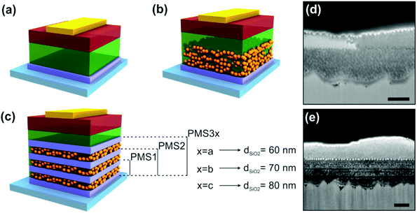 | ||
| Fig. 1 Scheme of the different perovskite solar cell architectures under analysis: (a) planar, (b) mesostructured, and (c) multilayer structure based configurations. See Table 1 for thickness information. (d) SEM picture of the reference device S. (e) SEM picture of the PMS-based device PMS3a. Scale bars represent 200 nm. | ||
Structural, optical and photovoltaic characterization
A combined focused ion beam-scanning electron microscope (FIB-SEM, Zeiss Auriga) was employed to estimate the thicknesses of the different layers composing the devices. Cross sections of the whole solar cells were obtained from a lamella prepared also with FIB in order to have a clean cut and thus prevent degradation of the materials and the collapse of the layers. Then, a secondary electron detector was used to take the images with the SEM operating at 5 kV.Characteristic perovskite crystal planes were observed with a transmission electron microscope (TEM, FEI Talos) equipped with a high angle annular dark field (HAADF) detector. Then, energy-dispersive X-ray spectroscopy (EDS) analysis was performed by scanning a 0.64 μm2 area of the cross-section of the device. The spot diameter for the elemental analysis was set to 3 nm.
Reflectance, transmittance and absorptance spectra were measured from 400 nm to 800 nm with a setup consisting of a light source (Ocean Optics HL-2000) as the incident beam and an integrating sphere (Labsphere RTC-060-SF) to collect photons coming from the solar cell device. This particular design of the setup allowed us to measure the fraction of diffuse light.
Current density–voltage (J–V) curves were obtained (2400 Series SourceMeter, Keithley Instruments) under simulated AM 1.5 irradiance at 100 mW cm−2 (Abet Class AAB sun 2000 simulator). An NREL calibrated KG5 filtered Si cell was used as a reference to calibrate the intensity, giving a mismatch factor of less than 1%. The active area of the devices was determined using a 0.092 cm2 mask.
Impedance and OCVD
Impedance spectroscopy measurements were carried out using a FRA equipped PGSTAT-30 from Autolab, under 100 mW cm−2 illumination conditions using a 150 W Xe lamp. A 20 mV AC perturbation was applied over the constant forward applied bias, between 0 V and 1 V, with the frequency ranging between 1 MHz and 0.05 Hz. OCVD measurements were recorded with the same Autolab system after switching off the illumination by employing a shutter. The voltage decay was recorded for 5 min. The devices were carefully treated under identical illumination conditions.Results and discussion
PSCs were prepared by depositing CH3NH3PbI3 perovskite precursors on porous substrates with different multilayered configurations, as shown in Fig. 1a. The configuration of the substrate, considered as a piece of transparent conducting glass onto which a series of compact electron selective layers and porous scaffolds are deposited, was systematically varied from sample to sample. On the other hand, the perovskite capping layer, the spiro-OMeTAD hole selective contact, and the Au hole extracting contact remained constant. Details of the thickness of all the different layers that form the devices under study are displayed in Table 1. Further details on sample preparation may be found in the Methods section. Two different sets of samples were prepared in order to confirm the trends observed, see ESI† for more data. Two kinds of reference samples with standard PSC architectures were prepared, namely, P samples, which are planar devices prepared using no scaffold and just a TiO2 compact layer as a selective electron contact deposited onto a FTO substrate (Fig. 1a), and S samples, which are PSCs made by depositing a SiO2 mesoporous scaffold on top of the TiO2 compact layer (Fig. 1b). In addition, PMSs were prepared by alternating SiO2/TiO2 bilayers (Fig. 1d). More specifically, PMS1, PMS2 and PMS3 were attained by successively stacking 1, 2 and 3 SiO2/TiO2 bilayers on top of the TiO2 layer used in the P configuration. By doing so, we intended to magnify the effect that the injection process may have on the performance of the device. For the case of the PMS-based devices presenting 3 SiO2/TiO2 bilayers, the thickness of the SiO2 scaffold was also varied (PMS3a, PMS3b and PMS3c, see Fig. 1d). This was done to extract information on the influence of the insulating mesoporous scaffold on the charge transport along the cell. All of the TiO2 layers were deposited following exactly the same procedure, so they present a similar thickness and low porosity in all cases.16,18 After perovskite infiltration, all of the devices presented a comparable light harvesting efficiency, i.e., absorptance, as was confirmed by optical analysis (please see the ESI,† Sections S1 and S2, and Fig. S1, as well as Table 1). Although the discussion of our results will mainly be based on the set of devices described in Table 1, we prepared another set with a different thickness of the TiO2 compact layers in the PMS in order to check the reproducibility of the analysis. For the sake of space, the structural features and the results of the characterization of those devices, corresponding to the second set of samples, are fully described in the ESI† (Tables S1, S2, Fig. S3a, S7, S8 and S10). Suffice it to say here that similar conclusions can be extracted from the analysis of both sets of devices.| P | S | PMS1 | PMS2 | PMS3c | PMS3b | PMS3a | |
|---|---|---|---|---|---|---|---|
| FTO thickness (nm) | 600 ± 60 | 600 ± 60 | 600 ± 60 | 600 ± 60 | 600 ± 60 | 600 ± 60 | 600 ± 60 |
| No. TiO2 layers | 1 | 1 | 2 | 3 | 4 | 4 | 4 |
| Total TiO2 thickness (nm) | 27 ± 3 | 27 ± 3 | 54 ± 6 | 81 ± 9 | 108 ± 12 | 108 ± 12 | 108 ± 12 |
| No. SiO2 layers | 0 | 1 | 1 | 2 | 3 | 3 | 3 |
| Total SiO2 thickness (nm) | 0 | 275 ± 35 | 80 ± 5 | 160 ± 10 | 240 ± 15 | 210 ± 15 | 180 ± 15 |
| Perovskite capping thickness (nm) | 245 ± 50 | 245 ± 50 | 245 ± 50 | 245 ± 50 | 245 ± 50 | 245 ± 50 | 245 ± 50 |
| Spiro-OMeTAD thickness (nm) | 485 ± 35 | 485 ± 35 | 485 ± 35 | 485 ± 35 | 485 ± 35 | 485 ± 35 | 485 ± 35 |
| Au thickness (nm) | 50 | 50 | 50 | 50 | 50 | 50 | 50 |
| Normalized absorptance | 1 | 0.83 | 0.95 | 0.96 | 0.99 | 0.94 | 0.95 |
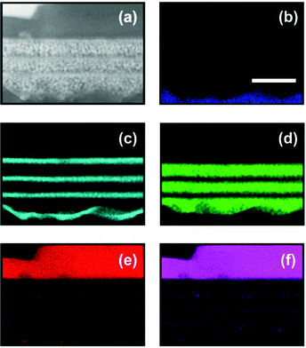
In order to determine how perovskite is distributed along the cross-section of the PMS-based devices, high resolution transmission electron microscopy (HRTEM) of the cells was performed. Fig. 2 shows a HRTEM picture of the cross-section of sample PMS3c, as well as the energy-dispersive X-ray spectroscopy (EDS) elementary analysis of Sn, Ti, Si, Pb and I evaluated from the same area. From these data it can be clearly recognized that, once the rough surface of the FTO substrate is leveled by the first layer of porous SiO2, flat and homogeneous TiO2 and SiO2 layers are produced. The perovskite precursors percolate the multilayered structure and crystallize appropriately within the SiO2 layers. Interestingly, the perovskite levels within the TiO2 layers are below the detection limit, although it must be present as its precursors embed the whole PMS. This observation suggests that, in PMS based devices, electrons may find an easier pathway to reach the electron collecting contact through the TiO2, rather than percolating through the low amount of infiltrated perovskite, increasing the ratio between the electrons injected into TiO2 and the electrons that had been transported just through the perovskite. This means that some of the electrons should experience more than one perovskite–TiO2, and vice versa, injection process in order to get to the FTO. This hypothesis is supported by recent experimental analysis that indicates that the energy levels of hybrid perovskite compounds and TiO2 are close.14 Indeed, the effect of electron injection processes is extraordinarily amplified in PMS based samples, as we show below, allowing us to study in depth its effect on the cell performance. At the same time the low amount of perovskite infiltrated into TiO2 allows the transport of holes to the collecting contact, although simultaneous transport through the TiO2 layers cannot be fully disregarded, as it has recently been demonstrated for electronically defective slabs.20 Please see Fig. S2 in the ESI† for a more detailed TEM analysis of the perovskite crystallization around the different interfaces.
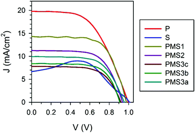
In order to test the validity of this hypothesis, we performed an analysis of the different photovoltaic parameters of the devices. From the analysis of the J–V curves, it could be readily inferred that the multilayered electrode configuration had a strong effect on the solar cell performance. Fig. 3 plots the J–V characteristics measured for the devices whose structural parameters are listed in Table 1 (see Fig. S3a for the J–V curves of the samples summarized in Table S1, ESI†). All of the analyzed samples present J–V curve hysteresis (see Fig. S3b, ESI†), mainly affecting the open circuit voltage (Voc) and fill factor (FF), as listed in detail in Table S3 (ESI†). The reverse scan of the S sample presents a photocurrent peak suggesting that, when operating under forward voltages, charge is accumulated in the device in such a way that, when the potential is reversed, it is delivered back.21,22 The most significant difference among all of the samples herein considered lies in the value of the short circuit photocurrent attained. The planar reference sample P is the one with the highest photocurrent, while the porous scaffold based sample S is the one with the lowest one. Interestingly the photocurrent gradually decreases for the samples with a PMS as the number of TiO2 layers and/or the thickness of the SiO2 scaffold increases. Among these two factors, the number of TiO2 layers is the factor that has a more significant effect. Please notice that although reduction of the photocurrent could be partially attributed to the small decrease in absorptance observed, see Table 1, this is by no means enough to explain its magnitude.
For a further verification of this hypothesis, open circuit voltage decay (OCVD) measurements were performed. This technique has been extensively utilized for the characterization of both dye sensitized23 and perovskite solar cells.24Fig. 4 plots the instantaneous relaxation time, τir, obtained from the data of the OCVD experiments, Fig. S4 (ESI†). A representation of the τir values against voltage in a log–log scale allows identification of the nature of the relaxation phenomena: constant τir values are obtained for exponential decay processes, while a straight line behavior is observed for processes following a power law.24Fig. 4a shows that the analyzed samples do not present these simplified relaxation behaviors. The devices display different relaxation domains with stretched exponential relaxation at the highest voltages in most of the cases, as has been already observed for other types of PSCs.24 Interestingly, it can be easily appreciated that there are significant differences among the samples (Fig. 4b). It can be observed that τir shifts to larger values as the number of TiO2 layers in the samples increases (please see dashed lines in Fig. 4b). However, varying the total thickness of the SiO2 scaffold for the samples built with four TiO2 layers, does not affect significantly τir. It is well known that the use of a compact TiO2 layer on top of FTO increases significantly the lifetime of the photocarriers in dye sensitized solar cells with OCVD, as this type of layer hinders the back-reaction from the substrate.25 In the same way, it can be concluded from the results shown in Fig. 4 that the increase of τir is due to the injection of electrons into TiO2, hindering the recombination with holes in the perovskite and slowing down the Voc decay. This observation hence indicates that the increase of the number of TiO2 layers in a device results in a gradual rise of the number of electron injection processes, as intended, thus magnifying their effect and opening the path to their systematic analysis.
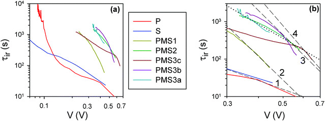 | ||
| Fig. 4 (a) Instantaneous relaxation time24 obtained from the data of OCVD experiments with a 5 minute decay time. (b) Zoomed-in view of the high voltage region in (a); the black dashed and dotted lines are guides for the eye. The dashed lines overlap, at high voltage, the curves for the samples with different numbers of TiO2 layers. The black dotted line connects the samples with 4 TiO2 layers, but different total thicknesses of SiO2. | ||
For further analysis, impedance spectroscopy (IS) under illumination was carried out for a series of different forward applied biases. Fig. 5 shows an example of the impedance patterns of the different samples attained using a DC applied voltage of 0.7 V. The patterns at short circuit can be found in Fig. S5 (ESI†). Similar patterns have been obtained from the second set of samples. Huge differences are observed in the IS pattern depending on the configuration of the electron selecting contact with the introduction of scaffold and/or multilayer structures. It should be remarked that all of the samples present a similar perovskite capping layer, as confirmed by the structural characterization analysis, which results in all of them presenting almost identical light harvesting efficiencies (please see Table 1). Hence, the scaffold mainly affects the electrical behavior of the cell. It modifies the electron selective contact properties, as has been previously hypothesized,26 and thus plays a determinant role in the cell performance and in the impedance spectra.15
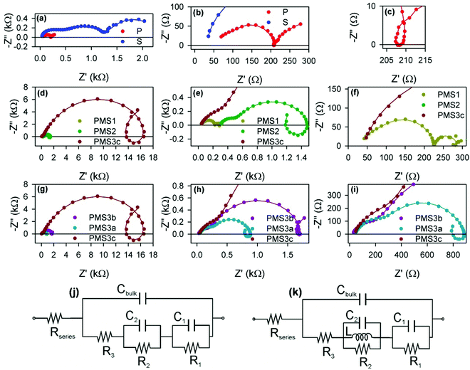 | ||
| Fig. 5 Nyquist plots of impedance spectra obtained under illumination and with an applied bias of 0.7 V. (a) Reference samples P and S. (b) Zoomed-in view of (a). (c) Zoomed-in view of the intermediate frequency loop of (a). (d) Samples with different numbers of TiO2 layers: PMS1, PMS2 and PMS3c. (e) and (f) Zoomed-in view of (d). (g) Samples with the same number of TiO2 layer, PMS3a, PMS3b and PMS3c, but different thicknesses of the SiO2 layers. (h) and (i) Zoomed-in view of (g). Equivalent circuits used to fit the impedance spectra when (j) no loop feature is observed, or (k) a loop is observed.15 The circles in (a)–(i) represent the experimental points, while the solid lines are the fitting curves using the equivalent circuits displayed in (j) and (k), but with non-ideal elements. See S6 for further information (ESI†). | ||
The impedance spectra present rich patterns, with several arcs and loops being displayed with positive imaginary impedance. The spectra were fitted using a recently reported equivalent circuit approximation analysis, see Fig. 5j and k.15 Briefly three arcs at different frequency domains can be observed for reference S, see Fig. 5a, and can be fitted with the equivalent circuit from Fig. 5j. The series resistance, Rseries, is produced by the effect of the FTO substrate and wiring, and can be extracted from the analysis of the high frequency region of the spectra (lower Z′ values). The diameter of the arcs determines the resistive elements: the successive arcs from high frequency to low frequency (low Z′ to high Z′) correspond to R3, R2 and R1, respectively. The frequency of the arc maximum and the resistance of each arc determine the capacitance values27 of Cbulk, C1 and C2. Cbulk is the geometric capacitance of the layer due to diverse dipolar mechanisms.15,28 Below we discuss the physical meaning of the other parameters.
Except for the case of reference sample P, the impedance spectra present very significant loops, as can be readily seen in Fig. 5c–e, g and h. The observation of such kinds of loops has already been reported for both highly efficient (∼17%) PSCs based on SnO2 and TiO2 electron selecting contacts15 and in devices in which the perovskite layer is sandwiched between FTO and Au contacts,29 although the magnitude we herein report is extraordinarily larger than those previously observed. This fact points to a general behavior of PSCs that sometimes could be concealed by other features. Indeed, some voltage must be applied when dealing with TiO2 electron selecting contacts in order to reduce the resistance that disguises the loop effect (please compare the impedance spectra of sample P at 0 V and 0.7 V, displayed in Fig. S5c (ESI†) and Fig. 5c respectively, for an illustrative example of this effect). This feature can be conveniently fitted by adding an inductive element, L, to the equivalent circuit, see Fig. 5k.15 Consequently, the choice of the type of equivalent circuit used to fit the impedance spectrum of a specific sample depends on the presence or not of loops in such patterns. Inductance versus applied voltage curves attained from the fitting of the impedance spectra of the different samples under illumination are plotted in Fig. 6. Fig. 6a shows a clear increase in L with the number of TiO2 layers. In contrast, the effect of the total thickness of mesoporous SiO2 is minor when the number of TiO2 layers is kept constant, see Fig. 6b. These results show a clear correlation between L and the electron injection processes, augmented with the number of TiO2 layers, and are in good qualitative agreement with inductive effects observed previously in impedance patterns of organic LEDs, which have been precisely attributed to a multistep injection process.30 In the case of organic LEDs, it has been shown that for certain cinematic conditions, it should be possible to depopulate the interfacial state when the applied voltage increases causing the negative capacitance,30i.e. the inductive behavior. Further research is required in order to clearly establish to what extent it is related to the oxide contacts or perovskite interfacial states, and to fully clarify the physical origin of this behavior. Similar trends and maximum values of L at 0.6 V were observed for the samples in the second batch (Fig. S7, ESI†).
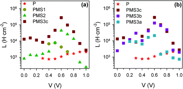 | ||
| Fig. 6 Inductance values obtained from the fit of the impedance spectra under illumination for the first set of samples, using the equivalent circuits plotted in Fig. 4. (a) Comparison of samples with different numbers of TiO2 layers; (b) comparison of samples with four TiO2 layers, but different total thicknesses of SiO2 scaffold. | ||
The rest of the resistive and capacitive parameters were also obtained by fitting the impedance patterns to the equivalent circuits plotted in either Fig. 5j or k. The resistance values are depicted in Fig. 7. The increase of R3 with the compact TiO2 layer thickness indicates that R3 is influenced by the transport resistance of electrons along the selective contact.15 In good agreement with this result, we observe a clear increase in R3 with the number of TiO2 layers, see Fig. 7a. Furthermore, when the thickness of the conductive TiO2 scaffold is kept constant, we observe that R3 is also modulated by the thickness of the insulating SiO2 scaffold infiltrated with perovskite (see Fig. 7d). This effect has not been reported yet, and it is clearly observed for the PMS3a, PMS3b and PMS3c samples containing four TiO2 layers, but also for reference samples P and S with just a single one. In this regard, it is well known that the charge diffusion lengths in perovskite infiltrated within a mesoporous scaffold are significantly lower than the ones observed for flat perovskite films.26 Consequently, we associate the R3 increase with the SiO2 scaffold thickness to a detrimental contribution of the charge transport along the perovskite infiltrated in the mesoporous layer. Compared to the case of planar perovskite layers, the higher transport resistance that we report is likely caused by the smaller perovskite grain size, due to the limited pore size of the mesoporous SiO2 layer. An analysis similar to the one herein presented was realized for the second set of samples, see Fig. S8 (ESI†), leading to similar conclusions.
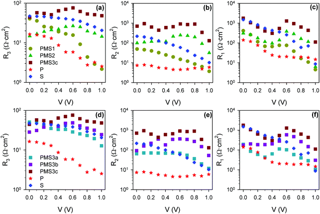 | ||
| Fig. 7 Resistance values obtained from the fitting of impedance spectra using the equivalent circuits plotted in Fig. 5j and k. (a) R3, (b) R2 and (c) R1 for the reference samples and PMS samples with different numbers of TiO2 layers. (d) R3, (e) R2 and (f) R1 for reference samples and PMS samples with the same number of TiO2 layers, but different thicknesses of the SiO2 layers. | ||
The low frequency resistance, R1, is typically considered to be an estimation of the recombination resistance,29,31–34 and the configuration of the electron selecting contact is known to dramatically affect the interfacial recombination resistance.29 Thus, we expect a strong dependence of R1 on the PMS parameters herein studied. Fig. 7c and f actually show an increase of R1 (reduction of recombination rate) as the number of TiO2 layers increases, but also as the total thickness of SiO2 increases, as can be clearly inferred from the comparison between the reference samples. This interpretation of the effect of R1 is in good agreement with the very close Voc observed for all the samples (Fig. 2 and Fig. S1a, ESI†), despite the different photocurrents.
Regarding R2, although there is significantly less discussion in the literature, it has been also related with recombination resistance,35 as well as with interfacial processes, as its presence and magnitude depend strongly on the electron selective material used in the PSC preparation.15,29 Notice that these two interpretations do not have to be mutually exclusive. From Fig. 7b and e it can be concluded that R2 presents a stronger dependence on the number of TiO2 layers, that is the number of perovskite–TiO2 interfaces, than on the total amount of SiO2, but it is influenced by both. Very recently, a correlation between high R2 values and low photocurrents has been highlighted.15 Interestingly, analogous correlation can be observed here, see Fig. 2 (Fig. S1, ESI†) and Fig. 7 (Fig. S8, ESI†) for the two sets of samples analyzed. It should be noted that R2 should not be considered merely a series resistance if the correlation with the photocurrent is finally confirmed, as this kind of resistance does not affect the photocurrent. Further research will be necessary in order to validate this correlation and, more importantly, to determine the physical origin of this resistive process (or processes).
Investigation of the capacitive values, displayed in Fig. 8, Fig. S9 and S10 (ESI†), also provides an interesting insight. As expected, Cbulk (Fig. S9a and c, ESI†) is a voltage independent parameter, confirming the interpretation of this capacitance as the geometrical capacitance of the layer.15 The low frequency capacitances, C1, present very high values that are heavily reliant on the applied bias conditions (Fig. 8).36 This capacitance is considered to be determined by majority carrier accumulation at the perovskite–compact TiO2 layer interface.37 Consequently, the contact materials, surface morphology and device configuration can affect these mechanisms. Indeed, a difference between the values corresponding to the PMS-based devices and those of reference cells P and S can be clearly observed, with the latter presenting a significantly lower C1 than the former, see Fig. 8a. Accumulation capacitance is proportional to the amount of charge,38 but charge accumulation must be compensated for by moving ions,37 which is actually the reason why its effect is detected at lower frequencies instead of at higher ones, as should be expected for electronic phenomena. Our results indicate a hindering of the ionic motion caused by the use of porous SiO2 scaffolds as a possible cause of the observed behavior. The systematic decrease of C1 with the increase of the total amount of SiO2 observed for all samples regardless of the number of TiO2 layers (Fig. 8a and b, respectively) also points in the same direction.
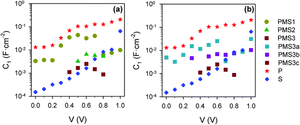 | ||
| Fig. 8 Capacitance values obtained from the fitting of impedance spectra using the equivalent circuits plotted in Fig. 5j and k. (a) C1 for the reference samples and PMS samples with different numbers of TiO2 layers. (b) C1 for the reference samples and PMS samples with the same number of TiO2 layers, but different thicknesses of the SiO2 layers. | ||
Interestingly, C2 has the opposite behavior comparing reference samples P and S (Fig. S9b, ESI†). This result allows identifying C2 as a surface state capacitance, considering not only the perovskite–TiO2 but also the perovskite–SiO2 interface. Capacitance C2 for PMS-based devices, built with the same number of TiO2 layers, takes values in between those obtained for both reference samples, although no clear trend is observed. Note that the discussion about results obtained and summarized in Fig. 7 and 8, is perfectly matched and validated by the results obtained for the second set of samples (Fig. S8 and S10, ESI†).
After the early report of non-transporting scaffolds prepared with alumina5 and the preparation of efficient planar PSCs,8 it seemed that the unique role of the mesoporous frame was to favor the growth of a uniform and pinhole-free perovskite layer. In spite of having demonstrated the viability of flat perovskite films as efficient photovoltaic materials, it seems that the presence of a thin TiO2 mesoporous scaffold still helps devices to reach higher efficiencies and low hysteresis. In fact, all of the certified record efficiency PSCs contain a thin mesoporous TiO2 scaffold followed by a thick perovskite capping layer on top.11,39–41 Our results indicate that the role of the scaffold goes beyond just providing a suitable matrix to grow perovskite crystals and influencing their geometry. The presence of the scaffold hinders and/or reduces the ionic migration, as can be deduced from the behavior of the C1 capacitance. This fact has two important effects. On the one hand, the presence of the scaffold reduces charge accumulation at the TiO2/perovskite interface (as a lower C1 is reported when a scaffold is present, see Fig. 8) and interfacial recombination, as its rate depends on carrier density, Fig. 7c and f. On the other hand, as ion migration has been signaled as the main source of hysteresis,42–45 the thickness of the scaffold should strongly influence this effect. Extrapolation of these results could help in understanding the observed effect of the scaffold on hysteresis reduction.10,11 However, the use of a scaffold also introduces a deleterious effect, as has been detected by the increase of the R1 and R2 resistances. The tortuosity of the scaffold not only hinders the motion of ions, but also that of electrons and holes, resulting overall in a transport resistance increase. An optimum cell design requires an appropriate balance between the lower recombination and hysteresis provided by the scaffold, but keeping the transport losses low in order to avoid the decrease of the diffusion length. This compromise requires the use of thin scaffolds, like the ones presented in the devices exhibiting the highest efficiencies.10,13,37,38
Conclusions
We have employed compact TiO2 and mesoporous SiO2 layers combined in different configurations in order to systematically characterize the impedance of perovskite solar cells. In particular, our experimental method allows the fabrication of periodic multilayer scaffolds, which enables the presence of a tailored number of perovskite–TiO2 interfaces within the device. This architecture boosts the injection effects, as indicated by open circuit voltage decay measurements, opening a novel path for their study in detail. We observe an inductive loop in the impedance spectra that becomes more evident when the number of perovskite–TiO2 interfaces increases. This anomalous injection behavior is the result of a multistep injection process. Moreover, we have observed that far from the optimum situation in which every single feature in the impedance pattern is produced by a single physical process, perovskite solar cells present complex spectra in which a single feature is affected by different processes. As a matter of fact, we demonstrate that R3, which has been previously related to the transport at the electron selective contact, is also influenced by transport taking place in the perovskite infiltrated within the mesoporous scaffold. Another interesting trend has been extracted from the analysis of impedance characterization herein reported: the reduction of the low frequency capacitance when a mesoporous SiO2 scaffold is introduced in the system points to a hindering of ionic migration and, consequently, majority charge accumulation at perovskite–TiO2 interfaces.37 This observation could have important implications in the search for configurations in which recombination and hysteresis are reduced, although it should also be noted that the scaffold also has a deleterious effect due to an increase in transport losses. An appropriate balance of both effects is therefore required. In this context, the continuous thinning of the mesoporous scaffold reported for perovskite based devices with the highest certified efficiencies can be appropriately understood.11,39,40 Our work constitutes a step towards the completion of the puzzle that impedance modeling and charge carrier transport in perovskite solar cells represent nowadays. We foresee that our conclusions on the anomalous injection detected in perovskite devices and the scaffold effect will have important implications for understanding their working principles and consequently for their further optimization.Acknowledgements
The research leading to these results received funding from the European Research Council under the European Union's Seventh Framework Program (FP7/2007–2013)/ERC grant agreement no. 307081 (POLIGHT) and the Spanish Ministry of Economy and Competitiveness under grants MAT2014-54852-R and MAT2015-70611-ERC. MA is grateful to “La Caixa” Foundation and VPPI of the University of Seville for their financial support. Structural characterization was performed at CITIUS, and we are grateful for their support. B. C. H. is grateful for the support of the National Council of Technological and Scientific Development (CNPq), Brazil, through the Science without Borders program.References
- http://www.nrel.gov/ncpv/images/efficiency_chart.jpg .
- A. Kojima, K. Teshima, Y. Shirai and T. Miyasaka, J. Am. Chem. Soc., 2009, 131, 6050–6051 CrossRef CAS PubMed.
- J.-H. Im, C.-R. Lee, J.-W. Lee, S.-W. Park and N.-G. Park, Nanoscale, 2011, 3, 4088–4093 RSC.
- H.-S. Kim, C.-R. Lee, J.-H. Im, K.-B. Lee, T. Moehl, A. Marchioro, S.-J. Moon, R. Humphry-Baker, J.-H. Yum, J. E. Moser, M. Gratzel and N.-G. Park, Sci. Rep., 2012, 2, 591 Search PubMed.
- M. M. Lee, J. Teuscher, T. Miyasaka, T. N. Murakami and H. J. Snaith, Science, 2012, 338, 643–647 CrossRef CAS PubMed.
- J. M. Ball, M. M. Lee, A. Hey and H. J. Snaith, Energy Environ. Sci., 2013, 6, 1739–1743 CAS.
- J. H. Heo, S. H. Im, J. H. Noh, T. N. Mandal, C.-S. Lim, J. A. Chang, Y. H. Lee, H.-J. Kim, A. Sarkar, M. K. Nazeeruddin, M. Gratzel and S. I. Seok, Nat. Photonics, 2013, 7, 486–491 CrossRef CAS.
- M. Liu, M. B. Johnston and H. J. Snaith, Nature, 2013, 501, 395–398 CrossRef CAS PubMed.
- H.-S. Kim, I. Mora-Sero, V. Gonzalez-Pedro, F. Fabregat-Santiago, E. J. Juarez-Perez, N.-G. Park and J. Bisquert, Nat. Commun., 2013, 4, 2242 Search PubMed.
- H.-S. Kim and N.-G. Park, J. Phys. Lett., 2014, 5, 2927–2934 CAS.
- N. J. Jeon, J. H. Noh, Y. C. Kim, W. S. Yang, S. Ryu and S. I. Seok, Nat. Mater., 2014, 13, 897–903 CrossRef CAS PubMed.
- C. Tao, S. Neutzner, L. Colella, S. Marras, A. R. Srimath Kandada, M. Gandini, M. D. Bastiani, G. Pace, L. Manna, M. Caironi, C. Bertarelli and A. Petrozza, Energy Environ. Sci., 2015, 8, 2365–2370 CAS.
- K. Wojciechowski, S. D. Stranks, A. Abate, G. Sadoughi, A. Sadhanala, N. Kopidakis, G. Rumbles, C.-Z. Li, R. H. Friend, A. K. Y. Jen and H. J. Snaith, ACS Nano, 2014, 8, 12701–12709 CrossRef CAS PubMed.
- J. P. Correa Baena, L. Steier, W. Tress, M. Saliba, S. Neutzner, T. Matsui, F. Giordano, T. J. Jacobsson, A. R. Srimath Kandada, S. M. Zakeeruddin, A. Petrozza, A. Abate, M. K. Nazeeruddin, M. Gratzel and A. Hagfeldt, Energy Environ. Sci., 2015, 8, 2928–2934 CAS.
- A. Guerrero, G. Garcia-Belmonte, I. Mora-Sero, J. Bisquert, Y. S. Kang, T. J. Jacobsson, J.-P. Correa-Baena and A. Hagfeldt, J. Phys. Chem. C, 2016, 120, 8023 CAS.
- M. Anaya, A. Rubino, M. E. Calvo and H. Miguez, J. Mater. Chem. C, 2016, 4, 4532–4537 RSC.
- C. Lopez-Lopez, S. Colodrero, M. E. Calvo and H. Miguez, Energy Environ. Sci., 2013, 6, 1260–1266 CAS.
- W. Zhang, M. Anaya, G. Lozano, M. E. Calvo, M. B. Johnston, H. Míguez and H. J. Snaith, Nano Lett., 2015, 15, 1698–1702 CrossRef CAS PubMed.
- S. H. Hwang, J. Roh, J. Lee, J. Ryu, J. Yun and J. Jang, J. Mater. Chem. A, 2014, 2, 16429–16433 CAS.
- S. Hu, M. R. Shaner, J. A. Beardslee, M. Lichterman, B. S. Brunschwig and N. S. Lewis, Science, 2014, 344, 1005–1009 CrossRef CAS PubMed.
- F. Fabregat-Santiago, I. Mora-Seró, G. Garcia-Belmonte and J. Bisquert, J. Phys. Chem. B, 2003, 107, 758–768 CrossRef CAS.
- J. Bisquert, F. Fabregat-Santiago, I. Mora-Seró, G. Garcia-Belmonte, E. M. Barea and E. Palomares, Inorg. Chim. Acta, 2008, 361, 684–698 CrossRef CAS.
- J. Bisquert, A. Zaban, M. Greenshtein and I. Mora-Seró, J. Am. Chem. Soc., 2004, 126, 13550–13559 CrossRef CAS PubMed.
- L. Bertoluzzi, R. S. Sanchez, L. Liu, J.-W. Lee, E. Mas-Marza, H. Han, N.-G. Park, I. Mora-Sero and J. Bisquert, Energy Environ. Sci., 2015, 8, 910–915 CAS.
- P. J. Cameron and L. M. Peter, J. Phys. Chem. B, 2005, 109, 7392–7398 CrossRef CAS PubMed.
- A. Listorti, E. J. Juarez-Perez, C. Frontera, V. Roiati, L. Garcia-Andrade, S. Colella, A. Rizzo, P. Ortiz and I. Mora-Sero, J. Phys. Lett., 2015, 6, 1628–1637 CAS.
- F. Fabregat-Santiago, G. Garcia-Belmonte, I. Mora-Seró and J. Bisquert, Phys. Chem. Chem. Phys., 2011, 13, 9083–9118 RSC.
- O. Almora, I. Zarazua, E. Mas-Marza, I. Mora-Sero, J. Bisquert and G. Garcia-Belmonte, J. Phys. Lett., 2015, 6, 1645–1652 CAS.
- E. J. Juarez-Perez, M. Wuβler, F. Fabregat-Santiago, K. Lakus-Wollny, E. Mankel, T. Mayer, W. Jaegermann and I. Mora-Sero, J. Phys. Lett., 2014, 5, 680–685 CAS.
- J. Bisquert, G. Garcia-Belmonte, Á. Pitarch and H. J. Bolink, Chem. Phys. Lett., 2006, 422, 184–191 CrossRef CAS.
- A. Dualeh, T. Moehl, N. Tétreault, J. Teuscher, P. Gao, M. K. Nazeeruddin and M. Grätzel, ACS Nano, 2014, 8, 362–373 CrossRef CAS PubMed.
- V. Gonzalez-Pedro, E. J. Juarez-Perez, W.-S. Arsyad, E. M. Barea, F. Fabregat-Santiago, I. Mora-Sero and J. Bisquert, Nano Lett., 2014, 14, 888–893 CrossRef CAS PubMed.
- B. Suarez, V. Gonzalez-Pedro, T. S. Ripolles, R. S. Sanchez, L. Otero and I. Mora-Sero, J. Phys. Lett., 2014, 5, 1628–1635 CAS.
- A. Pockett, G. E. Eperon, T. Peltola, H. J. Snaith, A. Walker, L. M. Peter and P. J. Cameron, J. Phys. Chem. C, 2015, 119, 3456–3465 CAS.
- E. Guillén, F. J. Ramos, J. A. Anta and S. Ahmad, J. Phys. Chem. C, 2014, 118, 22913–22922 Search PubMed.
- E. J. Juarez-Perez, R. S. Sanchez, L. Badia, G. Garcia-Belmonte, Y. S. Kang, I. Mora-Sero and J. Bisquert, J. Phys. Lett., 2014, 5, 2390–2394 CAS.
- I. Zarazua, J. Bisquert and G. Garcia-Belmonte, J. Phys. Lett., 2016, 7, 525–528 CAS.
- W. Mönch, Semiconductor Surfaces and Interfaces, Berlin, 1993 Search PubMed.
- W. S. Yang, J. H. Noh, N. J. Jeon, Y. C. Kim, S. Ryu, J. Seo and S. I. Seok, Science, 2015, 348, 1234–1237 CrossRef CAS PubMed.
- N. J. Jeon, J. H. Noh, W. S. Yang, Y. C. Kim, S. Ryu, J. Seo and S. I. Seok, Nature, 2015, 517, 476–480 CrossRef CAS PubMed.
- D. Bi, W. Tress, M. I. Dar, P. Gao, J. Luo, C. Renevier, K. Schenk, A. Abate, F. Giordano, J.-P. Correa Baena, J.-D. Decoppet, S. M. Zakeeruddin, M. K. Nazeeruddin, M. Grätzel and A. Hagfeldt, Sci. Adv., 2016, 2, e1501170 Search PubMed.
- E. L. Unger, E. T. Hoke, C. D. Bailie, W. H. Nguyen, A. R. Bowring, T. Heumuller, M. G. Christoforo and M. D. McGehee, Energy Environ. Sci., 2014, 7, 3690–3698 CAS.
- W. Tress, N. Marinova, T. Moehl, S. M. Zakeeruddin, M. K. Nazeeruddin and M. Gratzel, Energy Environ. Sci., 2015, 8, 995–1004 CAS.
- S. Meloni, T. Moehl, W. Tress, M. Franckevicius, M. Saliba, Y. H. Lee, P. Gao, M. K. Nazeeruddin, S. M. Zakeeruddin, U. Rothlisberger and M. Graetzel, Nat. Commun., 2016, 7, 10334 CrossRef CAS PubMed.
- G. Richardson, S. E. J. O'Kane, R. G. Niemann, T. A. Peltola, J. M. Foster, P. J. Cameron and A. B. Walker, Energy Environ. Sci., 2016, 9, 1476–1485 CAS.
Footnote |
| † Electronic supplementary information (ESI) available. See DOI: 10.1039/c6tc04639h |
| This journal is © The Royal Society of Chemistry 2017 |

