
 Open Access Article
 This Open Access Article is licensed under a
 Creative Commons Attribution 3.0 Unported Licence
Zinc diketonates as single source precursors for ZnO nanoparticles: microwave-assisted synthesis, electrophoretic deposition and field-effect transistor device properties†
Rudolf C.
Hoffmann
a,
Shawn
Sanctis
a,
Emre
Erdem
b,
Stefan
Weber
b and
Jörg J.
Schneider
 *a
*a
aDepartment of Chemistry, Eduard-Zintl-Institute, Inorganic Chemistry, Technische Universität Darmstadt, Alarich-Weiss-Straße 12, 64287 Darmstadt, Germany. E-mail: joerg.schneider@ac.chemie.tu-darmstadt.de
bInstitut für Physikalische Chemie, Albert-Ludwigs Ludwigs-Universität Freiburg, Alberstraße 21, 79104 Freiburg, Germany
First published on 19th July 2016
Abstract
The microwave-assisted decomposition of zinc diketonates in acetonitrile leads to stable dispersions of zinc oxide nanoparticles. The variation of the diketonato ligand framework permits controlling the size of primary crystallites and soft agglomerates, which allows the synthesis of nanoparticles in the range of 4–6 nm. Field-effect transistors are fabricated with charge carrier mobility as high as 0.32 cm2 V−1 s−1 and an Ion/off ratio of ∼106 after post-annealing at only 250 °C in air. Their superior performance is attributed to the dense packing of the ZnO particles in the semiconducting layer. Dispersions in aprotic solvent are suitable for a cathodic electrophoretic deposition of ZnO layers on ITO coated glass electrodes. Uniform ZnO coatings exhibiting interference colours can be obtained with thicknesses of several hundred nanometers.
Introduction
Zinc oxide provides one of the greatest assortments of varied particle morphologies occuring in one- (1D), two- (2D), and three-dimensional (3D) structures.1,2 Thus, a multitude of preparative strategies have been developed for the controlled formation of nanomaterials,3 but only a limited number of approaches are suitable for the solution-deposition of thin films in electronic applications.4 The desired functionality imposes a number of strict demands, which remain a challenge for the experimentalists.5 In a typical application ZnO nanoparticles should exhibit a morphology which allows uniform film formation with a high packing density. Furthermore, stable dispersions must be obtainable, which can be employed in commonly used deposition techniques. All this must be achieved without corruption of the electronic performance. Therefore typical synthetic procedures are disadvantageous, which apply larger and thus sterically demanding capping agents. In fact this necessarily introduces higher amounts of organic residues in the resulting films prepared therefrom.6 Furthermore, metathetical reactions must also be avoided, which could lead to contamination by alkali metals or halide ions.Recently, microwave-assisted routes for the synthesis of oxide nanoparticles by the decomposition of tailored molecular precusors have been suggested as a promising alternative. Rapid heating by microwaves ensures a high fraction of seeding particles and thus often a small particle size which is typically in the order of only several nanometers.7,8 Stabilisation of the nanoparticle dispersions is achieved by residual molecular fragments or solvents which remain on the particle surface.9–11
Herein we firstly report on the suitability of different zinc complexes with 1,3-diketonato ligands as single-source precursors for the microwave-assisted synthesis of dispersions of zinc oxide nanoparticles in acetonitrile. The influence of the systematic variation of the ligand framework on the size, morphology as well as the electronic properties of the obtained ZnO is investigated. Secondly, films can be obtained and employed as semiconducting layers in field-effect transistor devices (FET) which exhibit good performance. Thirdly, further work focuses on the electrophoretic deposition (EPD)12 of ZnO nanocrystals from stable dispersions onto indium tin oxide (ITO)-coated glass electrodes. The polar aprotic solvent which stabilizes the dispersions as well as the absence of foreign ions ensures low conductivity and thus allows the employment of higher voltages during the deposition.
Experimental
Precursors
Bis(acetylacetonato)zinc monohydrate (1) was purchased (Aldrich, 99.9%). Bis(methylacetato)zinc (2) and bis(dimethylmalonato)zinc (3) were synthesized by using a previously published procedure.13 All operations related to the synthesis of (2) and (3) were carried out under an inert atmosphere and with dry solvents. The final products were stored under argon in a glove box until further employment for the nanoparticle synthesis.Microwave reaction
Microwave reactions were carried out in a Discover (CEM) microwave reactor with original CEM reaction tubes and silicon stoppers supplied by the manufacturer. The precursors (1)–(3) were dissolved in acetonitrile (12.5 and 25 mM solutions). The resulting solution was filtered through a syringe filter and filled into the reaction tube (20 mL solution in 35 mL tubes). The solution was heated to the required temperature (160–220 °C) with a power of 300 W. The maximum temperature was reached in about 5 minutes. The vessel was then kept at this temperature for a further 25 minutes under constant microwave heating and was cooled afterwards to room temperature with compressive air cooling. The solvent was removed by condensation into a cold trap under vacuum which leads to a brownish residue, which was redispersed in tetrahydrofuran. The addition of pentane to the dispersion caused flocculation of an off-white precipitate, which was separated by centrifugation and dried in a drying cabinet at 100 °C for about 3 hours.FET measurements
FET-substrates (1.5 × 1.5 cm2, interdigital structure obtained from Fraunhofer IWS-Dresden, Germany) consisted of n-doped silicon with a 90 nm layer of SiO2, on which gold electrodes were deposited with an intermediate adhesive layer of indium tin oxide (ITO). The channel width of source/drain electrodes was W = 10 mm with a channel length L = 10 μm. FET substrates were cleaned by consecutive ultrasonication in acetone, 2-propanol and deionized water for 5 min and dried by purging with argon. The dispersions for deposition of ZnO were obtained from 12.5 mM solutions of the precursors (1) or (2), respectively, in acetonitrile and reaction in the microwave at 180 °C. Films were produced by spincoating (20 s at 2000 rpm) and heating on a hotplate for 4 min at elevated temperatures (250–450 °C) in air. By iteration of this coating procedure five layers were deposited in total. The film thicknesses were determined by AFM from scratched or etched edges and are between 28 and 35 nm for samples from different precursors and annealing at various temperatures.FET characteristics were determined using an HP 4155A Semiconductor Parameter Analyzer (Agilent) in a glove box in the dark under controlled conditions (argon, H2O exclusion). FET devices were stored in the dark for about 24 h prior to measurement to exclude photoconductive effects. Charge carrier mobility μSAT and the threshold voltage Vth were derived from a linear fitting of the square root of the source–drain current (IDS 0.5) as a function of gate–source voltage VGS.
Electrophoretic deposition
Electrodes (1.5 × 6 cm2) for the electrophoretic deposition consisted of a layer of 140 nm indium tin oxide on 0.4 mm soda lime glass. Zinc oxide dispersions were prepared from 25 mM solutions of (1) and reaction in the microwave at 180 °C. The electrodes were inserted (immersion depth ∼4 cm) into 40 mL of the ZnO dispersion in a beaker. The electrode distance was kept fixed at 1 cm. Deposition times were varied from 30 to 120 minutes with voltages from 20 to 40 V. The zinc oxide layer formed on the negative electrode (cathodic deposition). No obvious film formation was observed on the positive electrode.Characterisation
Atomic Force Microscopy (AFM): CP-II (Bruker-Veeco), tapping mode, 1 Hz, silicon cantilevers (T 3.75 μm, L 125 μm, W 35 μm, f0 300 kHz, k 40 N m−1). Thermogravimetry (TG): TG209F1-Iris (Netzsch). Samples were measured in oxygen at a heating rate of 10 °C min−1 in the range of 30–600 °C in aluminium crucibles. Dynamic Light Scattering (DLS): Zetasizer Nano (Malvern). Samples were measured in 10 mm quartz cuvettes. IR Spectroscopy: Nicolet 6700 (ThermoScientifc). Powders were measured using an Attenuated Total Reflection (ATR) unit. Transmission Electron Microscopy (TEM): Tecnai F20 (FEI) operated at 200 kV. Samples were supported on a lacey-carbon copper grid (300 mesh). Focussed Ion Beam (FIB): cross sections were prepared using a Helios Nanolab 400S (FEI). X-Ray diffraction (XRD): Miniflex 600 (Rigaku), Cu-Kα radiation, 600 W in the Bragg–Brentano geometry. Ellipsometry measurements were carried out using a Nanofilm_ep3 (Accurion) with the modelling software provided by the manufacturer. Curve fitting for the determination of the thickness of the ZnO layer was carried out using a three-layer model (glass substrate with ITO and ZnO films). Electron Paramagnetic Resonance (EPR): X-band (9.86 GHz) continuous-wave (cw)-EPR measurements were performed using a Bruker EMX spectrometer with a rectangular TE102 (X-band) resonator from Bruker. The offset in the magnetic field and the exact g-factors in X-band measurements were determined using a polycrystalline DPPH (2-diphenyl-1-picrylhydrazyl) reference sample with g-factor, g = 2.0036.Results and discussion
Precursor synthesis and particle formation
The precursor molecules were synthesized by reaction of diethyl zinc in pentane or hexane with the protonated form of the ligand (Scheme 1).13 The use of toluene, though, leads to incorporation of the latter as a solvate in the precipitate. For convenience, (1) was employed as the commercially available monohydrate in the following reactions. This material exhibited no obvious differences in comparison to batches obtained from the before-mentioned reaction. The course of the thermal decomposition was investigated in detail (Fig. 1 and Fig. S1, ESI†). Precursor (1) undergoes sublimation in dry oxygen (depicted for completeness in ESI,† Fig. S1). DSC investigations by other groups revealed several decomposition steps between 195 and 365 °C.14,15 Compounds (2) and (3) exhibited a gradual decay between 160 and 400 °C in several steps (Fig. 1). | ||
| Scheme 1 Synthesis of the precursors (1)–(3) from diethylzinc and the corresponding 1,3-diketone. | ||
 | ||
| Fig. 1 Thermogravimetric mass loss curve in air (solid black) and argon (solid grey) as well as the corresponding Gram–Schmidt signal (dashed) of (a) (2) and (b) (3). | ||
Although the course of the mass loss curves of (2) and (3) appeared to be very similar, an analysis of the volatile products by means of analysing them using TG-IR (Fig. 2 and 3) revealed different decomposition mechanisms. No obvious differences for the decomposition in oxygen in comparison to argon, however, were observed in the IR spectra for (2) as well as for (3). In the case of (2) the formation of methylacetate and methanol was detected besides decarboxylation. For (3) signals of dimethylmalonate (i.e. the ligand itself) were found at lower temperatures (about 175 °C, maximum in the Gram–Schmidt curve, i.e. the integrated intensity of the IR signals of the entire spectral range from 500 to 4000 cm−1) and no formation of carbon dioxide. The latter corresponds to our earlier investigations on the decomposition of metal complexes with 1,3-diketones with ester functionalities, in which similar rearrangements occurred.16,17
 | ||
| Fig. 2 Gas phase IR spectra corresponding to (a) the maximum of the Gram–Schmidt signal in Fig. 1a from the decomposition of precursor (2) as well as reference spectra of (b) methylacetate and (c) methanol. | ||
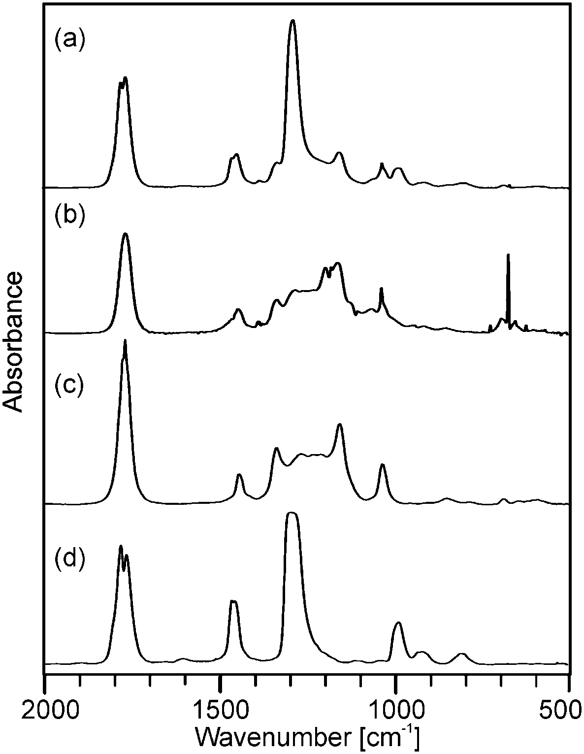 | ||
| Fig. 3 Gas phase IR spectra corresponding to (a) the maximum and (b) the right shoulder of the Gram–Schmidt signal in Fig. 1b from the decomposition of precursor (3) as well as the reference spectra of (c) dimethyl malonate and (d) dimethyl carbonate. | ||
The synthesis of spherical zinc oxide nanoparticles besides a number of platelet-shaped crystallites from the decomposition of (1) in acetonitrile in an autoclave at 100 °C over a period of two days was reported by Niederberger.18 Since acetonitrile possesses a dielectric constant κ of 37.5,7 a microwave-assisted route can be employed alternatively, which has the advantage of a drastic decrease in reaction time.
Obviously, a number of reaction parameters can be varied in the particle synthesis, such as precursor concentration and reaction temperature. The central aim, however, was to obtain dispersions with no larger agglomerates, as this is detrimental for application in substrate coating procedures. We found that following this paradigm prohibits very high precursor concentrations and reaction temperatures (Fig. 4).
 | ||
| Fig. 4 Hydrodynamic diameter determined by DLS for ZnO nanoparticles obtained from the decomposition of precursors (1) and (2) at concentrations of 12.5 and 25 mM in acetonitrile at various reaction temperatures. (Dotted lines are guides to the eye and have no physical meaning.) | ||
On the other hand lower concentrations resulted in an insufficient amount of solid material, whereas lower temperatures did not lead to detectable formation of oxide particles within reasonable reaction times (i.e. less than one hour). Best results with respect to particle size were obtained using concentrations of 12.5 and 25 mM as well as temperatures between 160 and 220 °C. Thereby almost clear or only slightly turbid dispersions could be synthesized using precursors (1) and (2). DLS investigations (Fig. 4) showed that monodisperse suspensions were formed containing particles in the range of 20 to 60 nm.
HRTEM (see below) confirmed that these are rather soft ZnO particle agglomerates. The removal of the solvent under vacuum leads to greasy residues, which could be redispersed in tetrahydrofuran. The particles were precipitated therefrom by the addition of pentane and subsequent centrifugation.
XRD diffractrograms (Fig. 5 and Fig. S2, ESI†) indicated reflections with a distinct line broadening, which can be attributed to the wurzite phase (JCPDS card 36-1451). Thereby samples from the microwave-assisted decomposition of (1) lead to significantly larger crystallites in comparison to those from the reaction of (2). ZnO powder samples obtained at reaction temperatures of 180 °C (corresponding to the conditions employed for dispersions used in FET fabrication) were investigated by means of TEM. The findings corresponded nicely to the XRD investigations giving a diameter of 13–16 nm for the crystallites (Fig. 6) in samples from (1) and 3–6 nm (Fig. 7) for those obtained from (2), respectively. The particles were spherical and had a narrow size distribution, but formed agglomerates after the removal of the solvent.
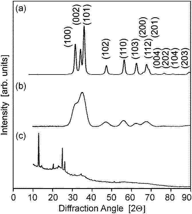 | ||
| Fig. 5 (a–c) X-ray diffractograms of ZnO powders obtained by the decomposition of the precursors (1)–(3) in acetonitrile (12.5 mM, 180 °C), respectively. | ||
 | ||
| Fig. 6 (a and b) HRTEM images at different magnifications of nanocrystalline zinc oxide obtained from microwave processing of the precursor (1) (12.5 mM, 180 °C). Inset in (a) shows the corresponding SAED pattern. | ||
 | ||
| Fig. 7 (a and b) HRTEM images at different magnifications of nanocrystalline zinc oxide obtained from microwave processing of precursor (2) (12.5 mM, 180 °C). Inset in (a) shows the corresponding SAED pattern. | ||
The reaction of acetonitrile solutions of (3) yielded only very turbid suspensions, from which yellow precipitates were isolated. The X-ray diffractrogram did not comprise reflections from zinc oxide, but from other crystalline compounds instead (Fig. 5c). The IR spectrum (ESI,† Fig. S3) exhibited no peak expected for ν(M–O) stretching vibrations at about 450 cm−1, but instead a prominent signal at 2180 cm−1, which could be assigned to a ν(C![[triple bond, length as m-dash]](https://www.rsc.org/images/entities/char_e002.gif) N) stretching vibration, was detected.19 This indicated the formation of zinc cyanide due to the cleavage of the solvent. Thus, under the employed conditions (3) is not a suitable precursor for zinc oxide. Furthermore this finding points to the fact that the choice of the appropriate ligand/solvent combination is crucial for steering the microwave reaction.
N) stretching vibration, was detected.19 This indicated the formation of zinc cyanide due to the cleavage of the solvent. Thus, under the employed conditions (3) is not a suitable precursor for zinc oxide. Furthermore this finding points to the fact that the choice of the appropriate ligand/solvent combination is crucial for steering the microwave reaction.
Electron paramagnetic resonance studies
The room temperature X-band continuous wave EPR spectrum of zinc oxide particles obtained from (1) consists of two distinct EPR lines. One appears at a higher magnetic field at g1 = 1.962 and the other one in the lower magnetic field region at g2 = 2.004. These two EPR signals have already been discussed within the concept of a core–shell model.10,20–22The core–shell model is a semi-empirical model for nanoparticles of compounds with a hexagonal structure that explains size effects based on EPR and PL results.21,22 The nanoparticle is thereby divided into a core with hexagonal symmetry, which is equal to the bulk material and a shell with a cubic structure. Due to their different chemical environments each of the intrinsic defect centers yields a distinctly different g-factor. In this model, the EPR signals at around g ∼ 1.96 and around g ∼ 2.00 can be assigned directly to the core and shell, respectively. In the case of the EPR spectrum of zinc oxide particles obtained from (2) we observed that the signal from the core at g = 1.962 disappeared. This proves that the defect concentrations localized at the core such as vacancies or interstitials are too low to detect by EPR while the detection limit of EPR spectroscopy is already very high at 10−11.23 Here the contribution to the EPR spectrum is only from the surface defects which give an EPR signal at g = 2.004 as well. However, the shape and the intensity of the signal assigned to these surface defects drastically change compared to the surface defect signal of ZnO from (1). This is mainly due to the change in particle size which correlates with a change of the number of defects due to size and also probably the change of the kinds of defects going from Zn vacancy to O vacancy or interstitials. Thus, it is a further proof for the before-mentioned finding that very small crystallites with a diameter below 6 nm are present in this sample. The broadening of the EPR signal of zinc oxide derived from precursor (1) in comparison to the ZnO derived from precursor (2) is also in agreement with the findings of the XRD studies which indicate a close relation of surface defects with size and structural changes.20,24 These findings already indicate a possible employment of the ZnO particles as a promising semiconductor material (Fig. 8).
 | ||
| Fig. 8 Room temperature X-band cw-EPR spectra of ZnO powders obtained by the decomposition of precursors (1) and (2) in acetonitrile (12.5 mM, 180 °C). | ||
Semiconducting properties and field effect transistor device studies
A series of FETs with a bottom gate/bottom contact setup (Fig. 9a) were manufactured by spincoating dispersions of nanoparticles from the microwave reaction of (1) and (2) on prefabricated substrates (support/gate highly n-doped silicon, dielectric silicon dioxide and interdigital gold electrodes). The films were obtained by spincoating and annealing on a hotplate at temperatures from 250 to 450 °C in air. | ||
Fig. 9 (a) Schematic setup of the FET device. (b and c) Performance of an FET with ZnO nanoparticles (12.5 mM, 180 °C) obtained from the microwave-assisted decomposition of precursor (2) and additional annealing at 250 °C in air. The ZnO film was deposited from five individual layers resulting in a total thickness of 33 nm. (b) Output characteristics obtained from variation of the drain–source voltage from 0 to 30 V for gate–source voltages from 0 to 30 V in 5 V steps. Data were acquired for increasing as well as decreasing drain–source voltages. (c) Transfer characteristics for the constant drain–source voltage of 25 V (μ 0.32 cm2 V−1 s−1, Vth + 16.4 V, Ion/off ratio ∼960![[thin space (1/6-em)]](https://www.rsc.org/images/entities/char_2009.gif) 000). 000). | ||
Additional calcination after the deposition of metal oxide nanoparticles might be required in order to remove the remaining solvent or other residual organics.6,25 However, acetonitrile is a low boiling solvent25 having the advantage of facile removal and low annealing times to obtain the final films. Furthermore annealing will affect the charge carrier concentration and is a valuable means to adjust the film composition and morphology towards an optimum of performance.10 Sintering is, however, not expected at such low temperatures.26
Films from nanoparticles derived from (1) exhibited only very low charge carrier mobilities after calcination at 250 and 350 °C below 0.02 cm2 V−1 s−1. After calcination at 450 °C, however, FETs exhibited a mobility μ of 0.21 cm2 V−1 s−1 with a threshold voltage Vth of +16.4 V and an Ion/off ratio of 750000 (ESI,† Fig. S4). In contrast, films (ESI,† Fig. S5) from nanoparticles of (2) showed a mobility μ of 0.32 cm2 V−1 s−1 with a threshold voltage Vth of +16.4 V and an Ion/off ratio of 960000 after calcination at only 250 °C (Fig. 9b and c). Annealing at higher temperatures did not lead to further improvement, but resulted in samples with no clear saturation in the transfer characteristics. Instead these samples rather showed a conductive behavior.
Comparisons with the work of other groups is complicated by the influence of the set-up and geometry on the electronic parameters. The employment of sol–gel procedures with annealing at temperatures above 500 °C can achieve charge carrier mobilities as high as 5–6 cm2 V−1 s−1.27 The comparison with investigations, in which the semiconducting layers likewise were built up from ZnO particles, seems to be more instructive. Thus larger particles (aggregates >50 nm) from a microwave-reaction of a precursor in methoxyethanol, exhibited a lower performance μ 0.045 cm2 V−1 s−1.10 In another investigation rod-like particles of a similar size (65 nm long and 10 nm wide) yielded comparable values of 0.023 cm2 V−1 s−1. Notably, an intricate post-deposition hydrothermal growth of additional ZnO to fill voids and calcination at 230 °C could raise the mobility to 0.65 cm2 V−1 s−1.28,29 By combining very small ZnO particles (∼3–4 nm) with an additional unreacted precursor in the deposition solution films with a higher density could be fabricated which exhibited charge carrier mobilities of 1.75 cm2 V−1 s−1 after processing at 250 °C.30
Thus, smaller particles, which allow a higher packing density, clearly offer a better performance. Possibly, the morphology as well as the size is of importance. Several authors report an improvement of the charge transport of rod-shaped particles in comparison to equally sized spherical counterparts.31,32
Electrophoretic deposition, EPD
Further investigations dealt with the formation of ZnO coatings on ITO coated glass substrates by means of EPD (Fig. 10a). The experiments were performed with ZnO dispersions in acetonitrile obtained from decomposition of (1). ZnO cathodic deposition was observed at DC voltages of 20 to 40 V and deposition times between 30 and 120 minutes. | ||
| Fig. 10 (a) Schematic depiction of the electrophoretic deposition process. (b) Film thickness of ZnO deposits obtained at different voltages (circles 20 V, squares 30 V and triangles 40 V) on ITO/glass substrates from nanoparticles synthesized from the microwave-assisted decomposition of (1) in acetonitrile. | ||
These conditions lead to adherent films exhibiting interference colours. Longer reaction times and higher voltages yielded thicker films, which can be peeled off the substrate after drying. Thinner ones adhered well to the substrate. The thickness of these adherent films was determined by ellipsometry (Fig. 10b) as well as SEM and HRTEM cross sections (Fig. 11). As expected, longer deposition times lead to a higher film thickness, whereby the growth rate decreased significantly with prolonged deposition time.33,34 SEM top views showed that higher voltages lead to more uniform films (ESI,† Fig. S6). Furthermore, longer deposition times lead to a higher surface roughness (ESI,† Fig. S7). It is noteworthy that in all cases a crack free, homogeneous surface coverage was observed and no larger agglomerates or other flaws in the as deposited layers were observed. A cross section of the thin film was prepared by means of the FIB technique. This allowed a more detailed HTREM investigation of the thin film layer deposited by EPD (Fig. 11).
 | ||
| Fig. 11 HRTEM images of a cross section prepared by FIB from ZnO films on ITO/glass substrates. Pt and Au are due to the FIB preparation procedure. The used ITO/glass substrates possess an anti-diffusion layer, ADL. The ZnO film was obtained after 30 minutes deposition time at 30 V. | ||
In support of the previous findings the images revealed a continuous layer with consistent thickness. High resolution TEM micrographs of the ZnO layer (ESI,† Fig. S8) allow characterization of the granular microcrystalline structure of the formed ZnO film. Although oriented attachment35–37 seems to occur in areas close to the surface, the overall film consists of randomly oriented ZnO crystallites.
Conclusions
Complexes of zinc with 1,3-diketonates are suitable as single-source precursors for solution processed zinc oxide nanoparticles. Thereby microwave heating of precursor solutions leads to stable dispersions which can be employed for the manufacturing of dense ZnO coatings. This process is fast, highly reproducible and avoids contamination by alkali metals. The variation of the ligand framework allows controlling the size of the crystallites which form in the decomposition reaction. In particular, ZnO crystallites with sizes below 5 nm are accessible and advantageous for the spincoating of semiconducting layers in a field effect transistor geometry. This is due to a high packing density of the ZnO nanoparticles. The performance of these dense ZnO layers is superior in comparison to films from larger particles as well as layers synthesized from the direct thermal decomposition of molecular precursors for ZnO. The latter process suffers from the generation of thin films with a significant porosity due to the evolution of volatile combustion products during film formation. The before-mentioned precursors are also compatible with aprotic, polar solvents such as acetonitrile, which are favorable for the manufacturing of coatings by means of electrophoretic deposition.Acknowledgements
JJS, RWH and SS acknowledge financial support through program DFG SPP 1576. TEM and FIB studies were performed at ERC Jülich under contract ERC-TUD1. We acknowledge technical staff at ERC Jülich for performing the FIB sample preparation and Dr J. Engstler (TUDa) for performing TEM experiments.References
- B. Ludi and M. Niederberger, Dalton Trans., 2013, 42, 12554–12568 RSC.
- Z. L. Wang, J. Phys.: Condens. Matter, 2004, 16, R829–R858 CrossRef CAS.
- S. Diodati, P. Dolcet, M. Casarin and S. Gross, Chem. Rev., 2015, 115, 11449–11502 CrossRef CAS PubMed.
- R. Pasquarelli, D. Ginley and R. O'Hayre, Chem. Soc. Rev., 2011, 40, 5406–5441 RSC.
- S. R. Thomas, P. Pattanasattayavong and T. D. Anthopoulos, Chem. Soc. Rev., 2013, 42, 6910–6923 RSC.
- T. V. Richter, F. Stelzl, J. Schulz-Gericke, B. Kerscher, U. Wurfel, M. Niggemann and S. Ludwigs, J. Mater. Chem., 2010, 20, 874–879 RSC.
- M. Baghbanzadeh, L. Carbone, P. D. Cozzoli and C. O. Kappe, Angew. Chem., Int. Ed., 2011, 50, 11312–11359 CrossRef CAS PubMed.
- Y. Zhu and F. Chen, Chem. Rev., 2014, 114, 6462–6555 CrossRef CAS PubMed.
- M. König, S. Höhn, R. Hoffmann, J. Suffner, S. Lauterbach, L. Weiler, O. Guillon and J. Rödel, J. Mater. Res., 2010, 25, 2125–2134 CrossRef.
- J. J. Schneider, R. C. Hoffmann, J. Engstler, A. Klyszcz, E. Erdem, P. Jakes, R.-A. Eichel, L. Pitta-Bauermann and J. Bill, Chem. Mater., 2010, 22, 2203–2212 CrossRef CAS.
- A. Famengo, S. Anantharaman, G. Ischia, V. Causin, M. M. Natile, C. Maccato, E. Tondello, H. Bertagnolli and S. Gross, Eur. J. Inorg. Chem., 2009, 5017–5028 CrossRef CAS.
- H. K. Yadav and V. Gupta, J. Appl. Phys., 2012, 111, 102809 CrossRef.
- D. Bekermann, D. Pilard and R. Fischer, ECS Trans., 2009, 25, 601–608 CAS.
- T. Arii and A. Kishi, J. Therm. Anal. Calorim., 2006, 83, 253–260 CrossRef CAS.
- S. Music, A. Saric and S. Popovic, Ceram. Int., 2010, 36, 1117–1123 CrossRef CAS.
- R. C. Hoffmann and J. J. Schneider, Eur. J. Inorg. Chem., 2014, 2241–2247 CrossRef CAS.
- R. C. Hoffmann and J. J. Schneider, Eur. J. Inorg. Chem., 2015, 4254–4259 CrossRef CAS.
- J. Buha, I. Djerdj and M. Niederberger, Cryst. Growth Des., 2007, 7, 113–116 CAS.
- G. W. Chantry and R. A. Plane, J. Chem. Phys., 1960, 33, 736–740 CrossRef CAS.
- E. Erdem, J. Alloys Compd., 2014, 605, 34–44 CrossRef CAS.
- H. Kaftelen, K. Ocakoglu, R. Thomann, S. Tu, S. Weber and E. Erdem, Phys. Rev. B: Condens. Matter Mater. Phys., 2012, 86, 014113 CrossRef.
- S. K. S. Parashar, B. S. Murty, S. Repp, S. Weber and E. Erdem, J. Appl. Phys., 2012, 111, 113712 CrossRef.
- P. Erhart, K. Albe and A. Klein, Phys. Rev. B: Condens. Matter Mater. Phys., 2006, 73, 9 Search PubMed.
- S. Repp and E. Erdem, Spectrochim. Acta, Part A, 2016, 152, 637–644 CrossRef CAS PubMed.
- R. Branquinho, D. Salgueiro, A. Santa, A. Kiazadeh, P. Barquinha, L. Pereira, R. Martins and E. Fortunato, Semicond. Sci. Technol., 2015, 30, 024007 CrossRef.
- S. Schwarz, A. M. Thron, J. Rufner, K. van Benthem and O. Guillon, J. Am. Ceram. Soc., 2012, 95, 2451–2457 CrossRef CAS.
- C. S. Li, Y. N. Li, Y. L. Wu, B. S. Ong and R. O. Loutfy, J. Mater. Chem., 2009, 19, 1626–1634 RSC.
- B. Sun and H. Sirringhaus, Nano Lett., 2005, 5, 2408–2413 CrossRef CAS PubMed.
- B. Q. Sun, R. L. Peterson, H. Sirringhaus and K. Mori, J. Phys. Chem. C, 2007, 111, 18831–18835 CAS.
- S. Y. Cho, Y. H. Kang, J. Y. Jung, S. Y. Nam, J. Lim, S. C. Yoon, D. H. Choi and C. Lee, Chem. Mater., 2012, 24, 3517–3524 CrossRef CAS.
- S. Oh, I. Jang, S. G. Oh and S. S. Im, Sol. Energy, 2015, 114, 32–38 CrossRef CAS.
- Y. J. Pu, N. Morishita, T. Chiba, S. Ohisa, M. Igarashi, A. Masuhara and J. Kido, ACS Appl. Mater. Interfaces, 2015, 7, 25373–25377 CAS.
- M. Verde, M. Peiteado, A. C. Caballero, M. Villegas and B. Ferrari, J. Colloid Interface Sci., 2012, 373, 27–33 CrossRef CAS PubMed.
- M. Verde, M. Peiteado, M. Villegas, B. Ferrari and A. C. Caballero, Mater. Chem. Phys., 2013, 140, 75–80 CrossRef CAS.
- G. Falk, J. Phys. Chem. B, 2013, 117, 1527–1536 CrossRef CAS PubMed.
- A. Singh, N. J. English and K. M. Ryan, J. Phys. Chem. B, 2013, 117, 1608–1615 CrossRef CAS PubMed.
- K. R. Kort and S. Banerjee, J. Phys. Chem. B, 2013, 117, 1585–1591 CrossRef CAS PubMed.
Footnote |
| † Electronic supplementary information (ESI) available: TGA of precursors, XRD and IR data for ZnO nanoparticles, AFM, FET characterisation, SEM and HTREM micrographs of films from EPD. See DOI: 10.1039/c6tc02489k |
| This journal is © The Royal Society of Chemistry 2016 |