
 Open Access Article
 This Open Access Article is licensed under a Creative Commons Attribution-Non Commercial 3.0 Unported Licence
Tuning the electronic properties of monolayer and bilayer PtSe2via strain engineering†
Pengfei
Li
a,
Lei
Li
b and
Xiao Cheng
Zeng
*ab
aHefei National Laboratory for Physical Sciences at Microscale and Department of Chemical Physics, University of Science and Technology of China, Hefei, Anhui 230026, China
bDepartment of Chemistry, University of Nebraska-Lincoln, Lincoln, Nebraska 68588, USA. E-mail: xzeng1@unl.edu
First published on 14th March 2016
Abstract
The recently synthesized monolayer PtSe2 belongs to the class of two-dimensional transition metal dichalcogenide (TMDC) materials (Nano Lett., 2015, 15, 4013). Based on first-principles calculations, we show that the band gaps of monolayer and bilayer PtSe2 can be tuned over a wide range via strain engineering. Both isotropic and uniaxial strains are investigated. For bilayer PtSe2, the vertical out-of-plane strain is also considered. In most cases, the strain can reduce the band gap except for the bilayer PtSe2 under the isotropic strain (ε ≤ 4%) for which the band gap can be slightly enlarged. Importantly, the monolayer can be transformed from the indirect-gap to the direct-gap semiconductor at the compressive strain of εy = −8%. Moreover, the bilayer can undergo the semiconductor-to-metal (S–M) transition at a critical vertical strain due to the chemical interaction (p orbital coupling) between the Se atoms of the two opposite layers. Overall, the ability to modulate the band gap of monolayer and bilayer PtSe2 over an appreciable range of strains opens up new opportunities for their applications in nanoelectronic devices.
Introduction
Two dimensional (2D) graphene has attracted intensive research interest over the past ten years1–5 due to its novel properties such as unconventional quantum Hall effect, superior electronic conductivity, and high mechanical strength. However, the zero-band gap apparently hinders the wide application of graphene in optoelectronic nanodevices. This situation has led to extensive efforts devoted to the exploration of other 2D materials with finite band gaps such as phosphorene,6–10 BN,11 transition-metal dichalcogenides (TMDCs),12–17 and transition-metal trichalcogenides (TMTCs).18,19 The general formula of 2D TMDCs is MX2, where M is a transition metal in groups 4–10 while X is a chalcogen. Depending on the combination of metal and chalcogen, bulk TMDCs display diverse properties, ranging from insulators (HfS2), semiconductors (MoS2, WS2), semimetals (WTe2, TiSe2), metals (NbS2, VSe2) to superconductors (NbSe2, TaS2).20 Low-dimensional counterparts of bulk MX2 may preserve certain bulk properties but can also bring new characteristics due to quantum confinement effects.21–23 For example, low-dimensional TMDCs can offer new opportunities for research in many fields, such as in catalysis, energy storage, sensing and electronic devices.To date, most experimental studies of 2D TMDCs have been mainly focused on semiconducting MX2 with group 6 transition metals (Mo, W), e.g., MoS2, MoSe2, and WSe2. Recently, many other monolayer TMDCs beyond MoX2 and WX2 have been shown to exhibit unique physical or chemical properties as well. Specifically, Wang et al. reported a newly synthesized PtSe2 monolayer.24 Unlike the conventional method for the fabrication of MX2 through exfoliation or chemical vapor deposition, the synthesis of PtSe2 can be achieved via the direct deposition of Se atoms on a Pt substrate. Through angle-resolved photoemission spectroscopy (ARPES) and band structure calculations, it is found that monolayer PtSe2 is a semiconductor, contrary to the semimetal properties of its bulk counterpart. Moreover, the photo-degradation experiment suggests that monolayer PtSe2 can serve as a visible light-driven photocatalyst.
Many previous theoretical studies25–28 have shown that the electronic structures of 2D TMDCs can be notably modified by external electric fields or by in-plane strains. In this study, we show the strain-dependent electronic properties of monolayer and bilayer PtSe2 on the basis of the first-principles computations. Both isotropic and uniaxial in-plane strains are considered. In addition, for the bilayer PtSe2, we also considered normal compressive strain (out-of-plane vertical strain). We found that monolayer PtSe2 can maintain its indirect semiconducting character under strain except for the uniaxial compressive strain beyond −8% along the y direction (see below for definition), which induce a transition from the indirect semiconductor to the direct one. In general, the strains can reduce the band gap of monolayer PtSe2 regardless of the magnitude and direction of the strain. Under an isotropic in-plane strain, the tensile strain appears to be more effective for reducing the band gap of monolayer PtSe2 than the compressive strain except for the case of 8% tensile strain. On the other hand, the trend is opposite in the case of uniaxial strain. For the bilayer PtSe2, the isotropic in-plane compressive strain can enlarge the band gap first and then reduce the band gap, while the isotropic tensile strain reduces the band gap continuously. Hence, the strain-engineering behavior of monolayer or bilayer PtSe2 is very different from that of MoS2.25 Furthermore, the reversible semiconductor-to-metal transition is predicted for the PtSe2 bilayer under normal compressive strain in the critical range of 0.4 < ε ≤ 0.45. The transition stems from the p orbital coupling of the inner Se atoms of the two layers.
Computational methods
All the calculations are performed using the density functional theory within the generalized gradient approximation, as implemented in the Vienna Ab initio Simulation Package (VASP) 5.3.3 code.29 The all-electron plane-wave basis set within the projector augmented wave (PAW) method is adopted with 5d96s1 and 4s24p4 treated as valence electrons for Pt and Se, respectively, and the Perdew–Burke–Ernzerhof (PBE) exchange–correlation functional is selected. The cutoff energy for expansion of the wavefunction into plane waves is set to be 360 eV, and a k-point set of 25 × 25 × 1 is used for total-energy computation and a dense k-point set of 40 × 40 × 1 is used for electronic structure computation. The conjugate-gradient scheme is employed for the geometric relaxation until the force on each atom is less than 0.01 eV Å−1, and the total energy change is less than 1 × 10⁻⁵ eV. Sufficient vacuum space (≥15 Å) is used along the z direction (normal to the 2D sheet) to avoid spurious interaction among the periodic images. The van der Waals interaction originating from dynamical correlations between fluctuating charge distributions cannot be effectively described by the PBE functional. Hence, we incorporate the van der Waals interactions by adding a semi-empirical dispersion potential (D) to the conventional Kohn–Sham DFT energy, through a pair-wise force field following the Grimme's DFT-D3 method.30Results and discussion
The bulk PtSe2 belongs to the D33d (P![[3 with combining macron]](https://www.rsc.org/images/entities/char_0033_0304.gif) m1) space group of the trigonal system.31 As shown in Fig. 1(a), the monolayer PtSe2 can be viewed as cleaved from the (0001) surface of the bulk PtSe2, where one Pt atom layer is sandwiched between two Se layers. The optimized lattice parameter is 3.75 Å, very close to the experimental value of 3.70 Å.24 The Pt–Se bond length and the total energy per atom of PtSe2versus isotropic in-plane strain are examined. As shown in Fig. 1(b), the Pt–Se bond length increases almost linearly with the increasing tensile strain, but shows a gentle decrease with the increasing compressive strain. The bond length alteration surely correlates with the energy change. As shown in Fig. 1(c), the isotropic strain shows asymmetric quadratic dependence on the total energy per atom. The energy is −4.576 eV per atom at the compressive strain ε = −8%, but is −4.602 eV per atom at the tensile strain of ε = 8%. Therefore, from the energetic point of view, the tensile strain is easier to implement than the compressive strain.
m1) space group of the trigonal system.31 As shown in Fig. 1(a), the monolayer PtSe2 can be viewed as cleaved from the (0001) surface of the bulk PtSe2, where one Pt atom layer is sandwiched between two Se layers. The optimized lattice parameter is 3.75 Å, very close to the experimental value of 3.70 Å.24 The Pt–Se bond length and the total energy per atom of PtSe2versus isotropic in-plane strain are examined. As shown in Fig. 1(b), the Pt–Se bond length increases almost linearly with the increasing tensile strain, but shows a gentle decrease with the increasing compressive strain. The bond length alteration surely correlates with the energy change. As shown in Fig. 1(c), the isotropic strain shows asymmetric quadratic dependence on the total energy per atom. The energy is −4.576 eV per atom at the compressive strain ε = −8%, but is −4.602 eV per atom at the tensile strain of ε = 8%. Therefore, from the energetic point of view, the tensile strain is easier to implement than the compressive strain.
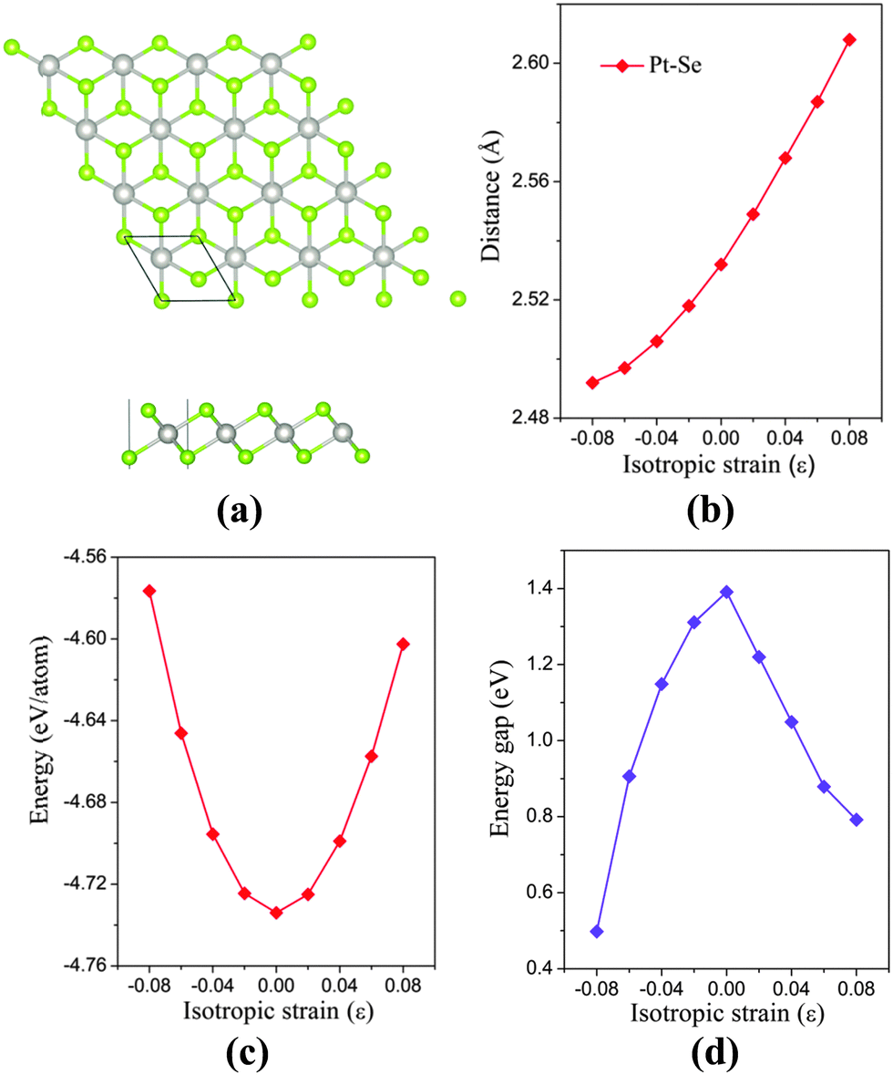 | ||
| Fig. 1 (a) Top and side views of monolayer PtSe2. The green and gray balls represent Pt and Se atoms, respectively. (b) Pt–Se bond length versus isotropic in-plane strain. (c) Total energy per atom of the monolayer PtSe2versus isotropic strain. (d) Computed band gap of monolayer PtSe2versus isotropic strain. | ||
The electronic structure of monolayer PtSe2 under the isotropic strain is shown in Fig. 2(a) and (b). The strain-free monolayer PtSe2 is an indirect semiconductor with a band gap of 1.39 eV, consistent with the previously predicted value of 1.41 eV (PBE).32 The valence band maximum (VBM) and conduction band minimum (CBM) are located at ΓH and TL points (see Fig. 2(a) and (b)), respectively. Upon increasing the compressive strain, the VBM remains at the ΓH point, while the CBM is shifted downward (Fig. 2(a)). When the compressive strain reaches −4%, the UL point exhibits lower energy than the TL point, leading to the relocation of the CBM. In contrast, as shown in Fig. 2(b), the tensile strain can significantly lower the position of ΓH point so that the VBM is shifted from the ΓH to the VH point whose energy remains unchanged, regardless of the tensile strain. In addition, the CBM (TL point) is shifted downward with the increasing tensile strain. In general, the band gap of the monolayer PtSe2 can be reduced by either the compressive or the tensile strain. As plotted in Fig. 1(d), the band gap of monolayer PtSe2 decreases linearly from 1.39 to 0.88 eV with the increasing tensile strain up to ε = 6%, and then to 0.79 eV at ε = 8%. However, the band gap of monolayer PtSe2 is correlated parabolically with the compressive strain, decreasing from 1.39 to 0.5 eV at ε = −8%. Moreover, it is known that semi-local DFT methods (such as the PBE functional) can markedly over-delocalize electrons. To address this issue, we performed an independent benchmark computation based on the DFT+U method as it can give more reasonable electronic properties than the semi-local DFT methods.33,34 We examined several values of U and found for U = 4 eV, the relaxed lattice constant of the monolayer PtSe2 is 3.725 Å, which is very close to the experimental value of 3.70 Å. The computed band structures of monolayer PtSe2 under the isotropic strain ε = −8%, 0% and 8% are plotted as shown in Fig. S1 (ESI†). It can be seen that the semiconducting character remains unchanged although the computed band gap is lowered by 0.1–0.4 eV for U = 4 eV.
 | ||
| Fig. 2 Computed band structures of monolayer PtSe2 under (a) isotropic compressive, and (b) isotropic tensile strain. The bands with different colors denote the band structures under different strain, i.e., blue (ε = 0%), cyan (ε = ± 2%), green (ε = ± 4%), yellow (ε = ± 6%) and red (ε = ± 8%). The Fermi level is located at 0 eV. | ||
To analyze the strain dependent electronic properties, the partial density of state (PDOS) and partial charge densities corresponding to the VBM and the CBM of the monolayer PtSe2 at the isotropic strain of −8%, 0% and 8%, respectively, are plotted as shown in Fig. 3(a)–(f). As shown in Fig. 3(b) and (e), for the strain-free monolayer, the VBM (ΓH point) is mainly contributed by Se p orbitals and the coupling between the Pt d orbitals (mainly dxy + dx2) and Se p orbitals. Yet the CBM (TL point) is mainly contributed by Pt dyz + dxz orbitals and, to less extent, by Se p orbitals and Pt dxy + dx2 orbitals. At the isotropic strain, as shown in Fig. 3(a), (c), (d) and (f), the VBM is mainly contributed by Se p orbitals and also slightly by Se-p and Pt-d coupling, different from the strain-free case. The isotropic strain significantly lowers the coupling between the Pt d orbitals and Se p orbitals near the VBM. However, the electronic component of the CBM under strain somewhat differs from that without strain. Fig. 2(a) and (b) clearly shows that, under isotropic strain, the change of band gap of monolayer PtSe2 is mainly induced by the location change of CBM. As shown in Fig. 3(f), at a tensile strain of 8%, the CBM (TL point) is mainly contributed by the Pt dxy + dx2 orbitals, Se p orbitals and somewhat by Pt dyz + dxz orbitals, apparently different from the case of zero strain. We therefore conclude that the electronic component of CBM is changed by the tensile strain, causing the descent of CBM energy and band gap reduction for the monolayer PtSe2. As for the monolayer PtSe2 under compressive strain, Fig. 3(d) shows that the electronic component of CBM is little changed, and is still contributed mainly by the Pt dyz + dxz orbitals. But the repulsion of charge density of the dyz + dxz orbitals can be enhanced under compressive strain, thereby lowering the CBM (UL point) and resulting in band gap reduction for the monolayer PtSe2.
 | ||
| Fig. 3 Partial charge densities corresponding to the VBM and CBM, and partial densities of states (PDOS) of the monolayer PtSe2 under isotropic strain of −8% (a and d), 0% (b and e) and 8% (c and f), respectively. Due to the specific symmetry, the contribution from dxy is the same as that from dx2, and the contribution from dyz is the same as that from dxz. The isosurface value is 0.001. | ||
We have also considered uniaxial strain along either the x or the y direction (see Fig. 4(a)). The computed electronic structure of the monolayer PtSe2 based on the rectangle supercell under the uniaxial strain are shown in Fig. 4(e)–(i) and in the ESI,† Fig. S2. At zero strain, the VBM is located at the ΓH point and the CBM at the AL point (Fig. 4(g)). As in the case of the isotropic strain, the uniaxial strain along either the x- or the y-direction can significantly lower the energy of CBM, but makes little change to the VBM (less than 50 meV), thereby reducing the band gap of the PtSe2 monolayer. Moreover, the uniaxial compressive strain along either the x- or the y-direction does not change the VBM position (always at the Γ point), similar to the case of isotropic strain. Interestingly, the monolayer PtSe2 undergoes the indirect-to-direct transition at the compressive strain of εy = −8% along the y direction, contrary to the isotropic strain. However, such a transition is not seen with the strain in the x direction even with a compressive strain of up to εx = −8%. In Fig. 4(d), the change in the energy value of AL and ΓL points (with respect to the Fermi level) is plotted as a function of the strain εy. It can be seen that the energy difference (EAL − EΓL) decreases almost linearly with the increasing compressive strain εy and becomes negative as εy is beyond −6%, causing an indirect-to-direct transition. Hence, we conclude that the indirect-to-direct transition can be attributed in part to the difference in strain dependence of EAL and EΓL. The curves of band gap of monolayer PtSe2versus uniaxial strain are plotted as shown in Fig. 4(c). Notably, the uniaxial strain along x- and y-directions results in exactly the same modulation to the band gap in the strain range of −6% (0.96 eV gap) to 4% (1.19 eV gap) and to strain 8% (0.94 eV gap). A slight difference is seen at the uniaxial strain of −8% and 6%, where the band gap Eg (εx = −8%) is 0.72 eV, Eg (εy = −8%) is 0.65 eV, Eg (εx = 6%) is 1.03 eV, and Eg (εy = 6%) is 1.10 eV. Fig. 4(b) shows the plot of Pt–Se bond length versus uniaxial strain, where the slope of the two curves is quite different. As a result, the monolayer PtSe2 shows direct semiconducting character at εy = −8% (Fig. 4(e)), but indirect semiconducting character at εx = −8% (Fig. 4(f)). In general, the uniaxial strain can modulate the band gap of the monolayer PtSe2 but less strongly compared to the isotropic strain. The specific uniaxial strain (εy = −8%), however, can transform the monolayer PtSe2 from an indirect semiconductor to a direct one.
 | ||
| Fig. 4 (a) A rectangle supercell of monolayer PtSe2 where x- and y-directions are defined. (b and c) Pt–Se bond length and band gap of monolayer PtSe2versus uniaxial strain, respectively. (d) The energy of the AL and ΓL points with respect to the Fermi level versus εy. Computed band structure of monolayer PtSe2 with strain values of (e) εy = −8%, (f) εx = −8%, (g) ε = 0%, (h) εx = 8% and (i) εy = 8%. The Fermi level is set to be 0 eV. | ||
The 2D bilayer materials may possess different electronic properties from the monolayer counterpart due in part to the weak van der Waals interlayer interaction. First, the electronic structures of bilayer PtSe2 under the isotropic strain are examined. Two different stacking patterns, namely, the AA-stacking and AB-stacking, are shown in Fig. 5(a). Our DFT computations show that both types of PtSe2 bilayers are almost degenerate in energy and also exhibit similar band structures. As shown in Fig. 5(c) and (e), both PtSe2 bilayers are indirect semiconductors with a band gap of 0.99 eV. The VBM and CBM are located at VH and TL points (see Fig. 5(c) and (e)), respectively. With the compressive strain, the position of VBM changes from the VH to the ΓH point but with small energy variation (<50 meV), while the CBM is kept at the TL point and moves up slightly for ε ≤ 4% and then downward to the Fermi level. As a result, the band gap of PtSe2 bilayers firstly increases for ε ≤ 4%, from 0.99 to 1.09 eV (see Fig. 5(b)) and then decreases for ε ≥ 4%, from 1.09 to 0.43 or 0.51 eV (Fig. 5(b)). Fig. 5(d) and (f) shows the tensile strain-dependent band structures of both PtSe2 bilayers, where one can see that the position of VBM moves slightly toward the K point with little energy change while the CBM is shifted toward the Fermi level. Therefore, the tensile strain reduces the band gap of PtSe2 bilayers from 0.99 eV to 0.48 or 0.56 eV (Fig. 5(b)).
 | ||
| Fig. 5 (a) Atomic structure of two kinds of PtSe2 bilayers. (b) Band gap of PtSe2 bilayers versus isotropic strain. Computed band structure of AA stacking bilayers under (c) ε = −8 to 0%, (d) ε = 0–8% and AB stacking bilayers under (e) ε = −8 to 0%, (f) ε = 0–8%. The bands with different colors represent the band structures under various strain values, i.e., blue (ε = 0%), green (ε = ±4%) and red (ε = ±8%). The Fermi level is located at 0 eV. | ||
Besides the in-plane strain, the electronic structures of the bilayer can also be modulated by applying an out-of-plane vertical strain. Taking the AB-stacking PtSe2 bilayer as an example, the vertical compressive strain (VCS) is defined as ε = (d0 − d)/d0 where d0 and d are the equilibrium and constrained interlayer distance, respectively. In the constrained configuration, the positions of the Pt atoms remain unchanged while other atoms are relaxed. The band structures of the bilayer under different VCS values are shown in Fig. 6(a)–(c), where it can be seen that the double degeneracy is lifted gradually due to the increasing interlayer chemical interaction as the interlayer distance decreases. The VBM is still located at the VH point with little change in energy, while the CBM (TL point) is shifted towards the Fermi level as the VCS increases, thereby reducing the band gap (Fig. 6(d)). It is interesting that the semiconductor-to-metal (S–M) transition occurs when the VBM and CBM crosses the Fermi level at the critical VCS (0.4 < ε ≤ 0.45; see Fig. 6(c)). To assess the experimental feasibility of the S–M transition, we estimated the required pressure as done previously by others.35,36 The applied pressure (P) is calculated from the energy cost per unit cell in reducing the interlayer distance by Δd = d0 − d, that is, P = (E0 − E)/((d0 − d) × A), where A is the area of unit cell, and E and E0 are the energies of strained and unstrained bilayers. As a result, the estimated transition pressure is between 1.2 and 3.6 GPa.
 | ||
| Fig. 6 (a–c) Computed band structure and partial densities of states of PtSe2 bilayer under three different VCS values, with the corresponding differential charge densities plotted in (e–g). The Fermi level is located at 0 eV. (d) Band gap of bilayer versus normal strain. | ||
To gain more insights into the electronic properties of the bilayer under VCS, the PDOSs are computed (Fig. 6(a)–(c)). With the increasing VCS, the contribution to the CBM from Pt d and Se p orbitals increases, while that to the VBM from Se p orbitals decreases. From Fig. 6(c), it is seen that density of states near the Fermi level is mostly contributed by Se p orbitals, giving the metal character of the bilayer. This is due to the enhanced interlayer interaction that leads to the p orbital interaction of the inner Se atoms of the two opposite layers. This conclusion can be further supported through redistribution of the charges, computed by taking the difference between the total charge of the bilayer and the two isolated PtSe2 layers (see Fig. 6(e)–(g)). The redistribution of the charge mainly arises around the inner Se atoms of the two layers. As expected, for a low VCS (ε ≤ 0.16), almost no charge redistribution is observed. With the increasing VCS, the degree of charge redistribution also increases, indicating enhanced Se–Se interaction which can lead to the S–M transition.
Conclusion
In conclusion, we investigate band-gap engineering of semiconducting PtSe2 monolayer and bilayer through applied isotropic, uniaxial, as well as vertical strains based on the first-principles calculations. Our electronic structure computations demonstrate that the electronic properties of PtSe2 monolayer and bilayer are dependent on both the magnitude and direction of the strain. As a result, the band gap can be tuned over a wide range. In addition, the PtSe2 monolayer can transform from an indirect semiconductor into a direct one when the compressive strain εy = −8%, which may be exploited for special applications in nanoelectronics. Furthermore, a reversible semiconductor-to-metal transition is predicted for the PtSe2 bilayer under critical VCSs (0.4 < ε ≤ 0.45, 1.2 GPa < P ≤ 3.6 GPa). This stems from the p orbital coupling of the inner Se atoms of the two layers. The possibility of reversibly tuning the band gap by about 1.0 eV through application of different strains will render the 2D PtSe2 a potential candidate for optoelectronic applications.Acknowledgements
P. F. Li and L. Li contributed equally to this work. This work was supported by USTC Qian-ren B Summer Research Fund and by the University of Nebraska's Holland Computing Center.References
- K. S. Novoselov, A. K. Geim, S. V. Morozov, D. Jiang, Y. Zhang, S. V. Dubonos, I. V. Grigorieva and A. A. Firsov, Science, 2014, 306, 666 CrossRef PubMed
.
- K. S. Novoselov, A. K. Geim, S. V. Morozov, D. Jiang, M. I. Katsnelson, I. V. Grigorieva, S. V. Dubonos and A. A. Firsov, Nature, 2005, 438, 197 CrossRef CAS PubMed
- K. S. Novoselov, E. McCann, S. V. Morozov, V. I. Falko, M. I. Katsnelson, U. Zeitler, D. Jiang, F. Schedin and A. K. Geim, Nat. Phys., 2006, 2, 177 CrossRef
- Y. B. Zhang, Y. W. Tan, H. L. Stormer and P. Kim, Nature, 2005, 438, 201 CrossRef CAS PubMed
- Q. Tang, Z. Zhou and Z. Chen, Nanoscale, 2013, 5, 4541 RSC
- L. Li, Y. Yu, G. J. Ye, Q. Ge, X. Ou, H. Wu, D. Feng, X. H. Chen and Y. Zhang, Nat. Nanotechnol., 2014, 9, 372 CrossRef CAS PubMed
- J. Dai and X. C. Zeng, J. Phys. Chem. Lett., 2014, 5, 1289 CrossRef CAS PubMed
- Y. H. Xu, J. Dai and X. C. Zeng, J. Phys. Chem. Lett., 2015, 6, 1996 CrossRef CAS PubMed
- M. H. Wu, H. Fu, L. Zhou, K. L. Yao and X. C. Zeng, Nano Lett., 2015, 15, 3557 CrossRef CAS PubMed
- H. Guo, N. Lu, J. Dai, X. J. Wu and X. C. Zeng, J. Phys. Chem. C, 2014, 118, 14051 CAS
- D. Pacile, J. C. Meyer, C. O. Girit and A. Zettl, Appl. Phys. Lett., 2008, 92, 133107 CrossRef
- B. Radisavljevic, A. Radenovic, J. Brivio, V. Giacometti and A. Kis, Nat. Nanotechnol., 2011, 6, 147 CrossRef CAS PubMed
- Q. H. Wang, K. Kalantar-Zadeh, A. Kis, J. N. Coleman and M. S. Strano, Nat. Nanotechnol., 2012, 7, 699 CrossRef CAS PubMed
- H. S. S. Ramakrishna Matte, A. Gomathi, A. K. Manna, D. J. Late, R. Datta, S. K. Patiand and C. N. R. Rao, Angew. Chem., Int. Ed., 2010, 49, 4059 CrossRef PubMed
- J. Feng, L. Peng, C. Wu, X. Sun, S. Hu, C. Lin, J. Dai, J. Yang and Y. Xie, Adv. Mater., 2012, 24, 1969 CrossRef CAS PubMed
- P. J. Jeon, S. Min, J. S. Kim, S. R. A. Raza, K. Choi, H. S. Lee, Y. T. Lee, D. K. Hwang, H. J. Choi and S. Im, J. Mater. Chem. C, 2015, 3, 2751 RSC
- H. Fang, S. Chuang, T. C. Chang, K. Takei, T. Takahashi and A. Javey, Nano Lett., 2012, 12, 3788 CrossRef CAS PubMed
- J. Dai and X. C. Zeng, Angew. Chem., Int. Ed., 2015, 54, 7572 CrossRef CAS PubMed
- M. Li, J. Dai and X. C. Zeng, Nanoscale, 2015, 7, 15385 RSC
- M. Chhowalla, H. S. Shin, G. Eda, L. Li, K. P. Loh and H. Zhang, Nat. Chem., 2013, 5, 263 CrossRef PubMed
- T. Cao, G. Wang, W. Han, H. Ye, C. Zhu, J. Shi, Q. Niu, P. Tan, E. Wang, B. Liu and J. Feng, Nat. Commun., 2012, 3, 887 CrossRef PubMed
- H. Zeng, J. Dai, W. Yao, D. Xiao and X. Cui, Nat. Nanotechnol., 2012, 7, 490 CrossRef CAS PubMed
- K. F. Mak, K. He, J. Shan and T. F. Heinz, Nat. Nanotechnol., 2012, 7, 494 CrossRef CAS PubMed
- Y. Wang, L. Li, W. Yao, S. Song, J. T. Sun, J. Pan, X. Ren, C. Li, E. Okunishi, Y. Q. Wang, E. Wang, Y. Shao, Y. Y. Zhang, H. Yang, E. F. Schwier, H. Iwasawa, K. Shimada, M. Taniguchi, Z. Cheng, S. Zhou, S. Du, S. J. Pennycook, S. T. Pantelides and H. J. Gao, Nano Lett., 2015, 15, 4013 CrossRef CAS PubMed
- P. Lu, X. Wu, W. Guo and X. C. Zeng, Phys. Chem. Chem. Phys., 2012, 14, 13035 RSC
- N. Lu, H. Guo, L. Li, J. Dai, L. Wang, W. Mei, X. Wu and X. C. Zeng, Nanoscale, 2014, 6, 2879 RSC
- A. Ramasubramaniam, D. Naveh and E. Towe, Phys. Rev. B: Condens. Matter Mater. Phys., 2011, 84, 205325 CrossRef
- P. Johari and V. B. Shenoy, ACS Nano, 2012, 6, 5449 CrossRef CAS PubMed
- G. Kresse and J. Furthmuller, Phys. Rev. B: Condens. Matter Mater. Phys., 1996, 54, 11169 CrossRef CAS
- S. Grimme, J. Antony, S. Ehrlich and S. Krieg, J. Chem. Phys., 2010, 132, 154104 CrossRef PubMed
- G. Y. Guo and W. Y. Liang, J. Phys. C: Solid State Phys., 1986, 19, 995 CrossRef CAS
- H. L. Zhuang and R. G. Hennig, J. Phys. Chem. C, 2013, 117, 20440 CAS
- V. I. Anisimov, F. Aryasetiawan and A. I. Lichtenstein, J. Phys.: Condens. Matter, 1997, 9, 767 CrossRef CAS
- P. Guss, M. E. Foster, B. M. Wong, F. P. Doty, K. Shah, M. R. Squillante, U. Shirwadkar, R. Hawrami, J. Tower and D. Yuan, J. Appl. Phys., 2014, 115, 034908 CrossRef
- L. Kou, B. Yan, F. Hu, S. Wu, T. O. Wehling, C. Felser, C. Chen and T. Frauenheim, Nano Lett., 2013, 13, 6251 CrossRef CAS PubMed
- L. Kou, S. Wu, C. Felser, T. Frauenheim, C. Chen and B. Yan, ACS Nano, 2014, 8, 10448 CrossRef CAS PubMed
Footnote |
| † Electronic supplementary information (ESI) available. See DOI: 10.1039/c6tc00130k |
| This journal is © The Royal Society of Chemistry 2016 |