Electrophoretic deposition of Ca2Nb3O10− nanosheets synthesized by soft-chemical exfoliation
Sang-Hyo
Kweon
a,
Mir
Im
b,
Woong-Hee
Lee
a,
Sahn
Nahm
*ab,
Ji-Won
Choi
c and
Seong-Ju
Hwang
d
aDepartment of Materials Science and Engineering, Korea University, Seoul 136-701, South Korea. E-mail: snahm@korea.ac.kr; Fax: +82 2 928 3584; Tel: +82 2 3290 3279
bKU-KIST Graduate School of Converging Science and Technology, Korea University, Seoul 136-701, South Korea
cElectronic Materials Center, Korea Institute of Science and Technology (KIST), Seoul 137-791, South Korea
dCenter for Intelligent Nano-Bio Materials (CINBM), Department of Chemistry and Nano Sciences, Ewha Womans University, Seoul 120-750, South Korea
First published on 25th November 2015
Abstract
Ca2Nb3O10− (CNO−) nanosheets exfoliated from a KCa2Nb3O10 ceramic were deposited on a Pt/Ti/SiO2/Si substrate at room temperature (RT) using the electrophoresis method, and subsequently annealed at various temperatures to remove organic defects. The inter-planar distance of the (001) plane of the CNO film deposited at RT was large (1.68 nm). This distance gradually decreased to 1.44 nm when the annealing temperature was increased to 600 °C due to the removal of organic defects. For CNO films annealed at temperatures higher than 600 °C, a CaNb2O6 secondary phase was formed, indicating that annealing should be conducted at 600 °C to obtain a homogeneous CNO film. Moreover, the CNO film annealed at 600 °C showed a large εr value of 65 with a low tan![[thin space (1/6-em)]](https://www.rsc.org/images/entities/char_2009.gif) δ of 0.01 at 1.0 MHz. This film also exhibited a high breakdown electric field of 0.43 MV cm−1 and a very low leakage current density of 3 × 10⁻⁸ A cm−2 at 0.4 MV cm−1.
δ of 0.01 at 1.0 MHz. This film also exhibited a high breakdown electric field of 0.43 MV cm−1 and a very low leakage current density of 3 × 10⁻⁸ A cm−2 at 0.4 MV cm−1.
Introduction
Demand for the miniaturization of electronic devices with performance enhancements has increased with the development of mobile electronic systems. In particular, size reduction of the capacitor is required for the miniaturization of electronic devices because the capacitor generally occupies a large area of the electronic device. A multilayer ceramic capacitor (MLCC) has been developed to achieve size reduction with performance enhancement of capacitors. BaTiO3 tape with a thickness close to 0.8 μm that was produced by 100 nm BaTiO3 nanoparticles with a large tetragonality (>1.008) has been used for the synthesis of an MLCC.1,2 Recently, a further reduction in the tape thickness with an increase of the capacitance has been called for.3 However, it is very difficult to synthesize a BaTiO3 tape thinner than 0.8 μm because of the difficulty of the synthesis of BaTiO3 nanoparticles smaller than 100 nm having a large tetragonality. In order to overcome this limitation, many efforts have been undertaken to produce thin film capacitors. (Ba1−xSrx)TiO3,4,5 Al2O3,6,7 TiO2,7,8 and HfO27 thin film capacitors have been extensively studied in an effort to satisfy these demands. However, the εr value of these films decreased with a reduction of the film thickness owing to the presence of a dead-layer.9–12 Moreover, the insulating properties of these thin films degraded when the film thickness was less than 10 nm, resulting in a large leakage current. Therefore, it is necessary to develop a new type of thin film material, which will maintain a high εr value with a low leakage current for use in high-performance MLCCs.13Recently, it has been reported that a very thin film (≤10 nm) with a high εr value can be grown using nanosheets that were delaminated from layered-structure compounds such as Ruddlesden–Popper, Aurivillius, and Dion–Jacobson materials.14–16 These materials generally have alkali metal or [Bi2O2]2+ ions in the layer between two perovskite slabs. Protons in acid solution can be substituted for these ions and the nanosheets then formed through an exfoliation process in which a proton is replaced by an organic polycation. Examples of such polycations are the tetrabutylammonium ion (TBA+) and poly(diallyldimethylammonium) ion (PDDA+).15–22 Finally, the nanosheets are deposited onto a substrate using various methods such as the Langmuir–Blodgett (LB) method and the layer-by-layer (LBL) method.15,18–22 Ti2NbO7− and Ca2Nb3O10− nanosheets were deposited on a SrRuO3 substrate using the LB method. They exhibited a high εr with a low leakage current density.21,22 The LBL method was used to grow a 10 nm-thick Ti0.87O2 film and it showed a εr of 125 and a leakage current density of 10−9–10−7 A cm−2 at 1 V.18 Although the nanosized thin films were well formed using both LB and LBL methods, a very long process time was required to obtain them. The deposition rate of the electrophoretic method is approximately 500 times larger than that of the LB and layer-by-layer methods.19,20 Moreover, it is possible to deposit nanosheets on an irregular-shaped electrode by using the electrophoretic method. Therefore, electrophoresis is a very useful deposition method for large-scale applications. Moreover, electrophoresis is an easy and convenient method to grow thin films using exfoliated nanosheets. For example, TiO2 thin films were formed on a Pt plate using H1.7Ti4O90.3− nanosheets by the electrophoresis method and their structural properties were reported.23 Other films also were grown by the electrophoresis method but the dielectric properties of these films have not been reported.24–27 In this work, Ca2Nb3O10 (CNO) films were grown on a Pt/Ti/SiO2/Si (Pt–Si) substrate by the electrophoresis method using CNO− nanosheets exfoliated from KCa2Nb3O10 (KCNO) ceramics. The growth process and the structural and electric properties of these CNO films were investigated.
Experimental section
KCNO precursor ceramics were synthesized by a conventional solid-state reaction. The detailed sintering processes of these KCNO ceramics have been reported in previous work.28 The sintered KCNO ceramics were stirred at 200 rpm in 2 M HCl for 7 days. A homogeneous protonic form of HCa2Nb3O10 (HCNO) was obtained after a filtration process. 0.1 g of HCNO was added into a vial that contained 20 mL of distilled water and an equivalent molar quantity of TBA+ ions. The TBA+ ions penetrated into the channel between two perovskite layers, resulting in the exfoliation of the CNO− nanosheets from the HCNO particles. Centrifugation was carried out to eliminate the un-reacted HCNO particles and the large CNO− nanosheets. All the electrophoretic thin films were grown in acetone, a polar solvent, to keep the CNO− nanosheets dispersed homogeneously in the electrophoresis solution. An electrical potential of 100 V was used to deposit the nanosheets on a Pt–Si substrate at RT. As-deposited CNO thin films were exposed to 200 W ultraviolet C light (main wavelength of 254 nm) to burn out the residual organic TBA+ cations. These films were annealed at 400–800 °C for 30 min under air. The structural properties of the films were examined using scanning electron microscopy (SEM: Hitachi S-4800, Japan), atomic force microscopy (AFM: Park systems NX-10), X-ray diffraction (XRD: Rigaku D/max-RC) and transmission electron microscopy (TEM: Jeol JEM 2100F). Thermogravimetric analysis (TGA: TA instruments Q50) and Fourier transform infrared spectroscopy (FTIR: Varian 640-IR) were carried out on colloidal suspensions annealed over the temperature range of RT–800 °C to examine the behavior of the organic components. To measure the dielectric properties over the frequency range from 75.0 kHz to 1.0 MHz, Pt was deposited on the films using conventional DC sputtering to form the top electrode of a metal–insulator–metal (MIM) capacitor. The top electrode was patterned using a shadow mask to form a 300 μm-diameter disk. The capacitance and the dissipation factor were measured using a precision LCR meter (Agilent 4285A, USA). The leakage current was measured by using a programmable electrometer (Keithley 6517B, USA).Results and discussion
Fig. 1(a) shows the XRD pattern of the KCNO ceramic precursor sintered at 1375 °C for 10 h after calcination at 900 °C. Therefore, all specimens were heated at 900 °C and subsequently annealed at 1375 °C. A homogeneous KCNO phase, which has a tetragonal structure with the lattice parameters of a = b = 0.77 nm and c = 2.95 nm, was well formed in this specimen without any secondary phases. Moreover, the intensity of the (00c) (c = 2, 4, 6, 8 and 14) peaks was very large, suggesting that most of the grains developed in this specimen had a large (002) plane. Fig. 1(b) shows the XRD pattern of the HCNO powders obtained from the sintered KCNO precursor after the exchange of K+ ions by H+ ions in HCl solution. This specimen showed a homogeneous HCNO phase that had a tetragonal structure with the lattice parameters of a = b = 0.39 nm and c = 1.44 nm. The HCNO powders obtained from the sintered KCNO exhibited high intensity (00l) (l = 1, 2, 3, 4 and 7) peaks, probably owing to the development of grains having a large (001) plane. The XRD patterns of the TBA+ and the mixture of CNO− nanosheets and TBA+ cations (TBA+/CNO−) are shown in Fig. 1(c). Two broad reflections with very low intensity were observed at approximately 11 and 25 degrees in the XRD pattern of TBA+. The XRD pattern of the TBA+/CNO− mixture is completely different from that of TBA+; a broad diffraction feature was observed below 10 degrees, indicating the presence of CNO− nanosheets without agglomeration such as osmotic swelling or restacking which cause reflections at low angles.29–31 The TBA+/CNO− mixture also showed broad reflections approximately at 12, 21, and 44 degrees, which were formed as a result of scattering from water and CNO− nanosheets.29 Peaks for the unreacted HCa2Nb3O10·5H2O phase were also observed but they were removed after filtration. Therefore, the XRD results show that the CNO− nanosheets were well synthesized from the sintered KCNO ceramics.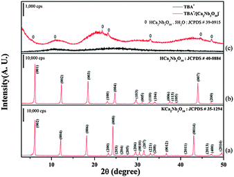 | ||
| Fig. 1 XRD pattern of (a) the KCNO precursor sintered at 1375 °C, (b) HCNO powders, and (c) the TBA+ cation and the mixture of CNO− nanosheets and TBA+ cations. | ||
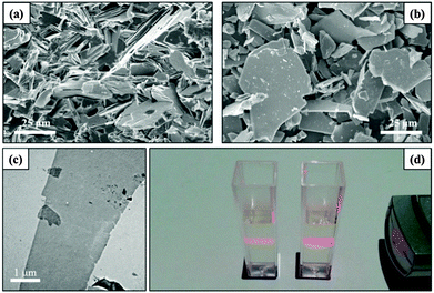
The SEM images of the fractured surface of the KCNO ceramic precursor sintered at 1375 °C and its protonic form, HCNO, are shown in Fig. 2(a) and (b), respectively. Very large grains (>20 μm) were formed in the sintered specimen, as shown in Fig. 2(a). Moreover, plate-shaped grains were well separated in an acid solution [see Fig. 2(b)], indicating that the protonation process hardly damaged the size of the grains. Fig. 2(c) shows a TEM bright-field image of the nanosheet. The size of this nanosheet was large. A Tyndall effect was observed from the colloidal suspension of the CNO− nanosheets, as shown in Fig. 2(d), confirming that the CNO− nanosheets were well formed in the colloid.
Fig. 3 shows the XRD patterns of the CNO thin films grown on Pt–Si substrates at RT and subsequently annealed at various temperatures. All the films annealed at temperatures lower than 700 °C showed XRD patterns of the homogeneous CNO phase. The inter-planar distance of the (001) plane of the CNO film deposited at RT was large, approximately 1.68 nm, and gradually decreased to 1.44 nm as the annealing temperature was increased to 600 °C. Defects such as TBA+ and H2O (or H3O+) were considered to remain between the CNO layers for the film deposited at RT, which resulted in a large inter-planer distance. However, these defects evaporated during annealing, resulting in a decrease of the inter-planar distance in the film. Since the variation of the inter-planar distance of the CNO films was not significant for the films annealed above 500 °C, most of the defects could be evaporated below 600 °C. For the films annealed at 700 °C, peaks for the CaNb2O6 phase were observed, although a small amount of the (001) peak for the CNO phase remained. Moreover, the peaks for the CaNb2O6 phase were observed only for the film annealed at 800 °C without a CNO phase. Therefore, annealing should be conducted at temperatures in the range of 500–600 °C to obtain a homogeneous CNO film.
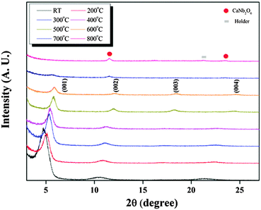 | ||
| Fig. 3 XRD patterns of CNO thin films grown on Pt–Si substrates at RT and subsequently annealed at various temperatures. | ||
TGA was also conducted on the colloidal aggregate of CNO− nanosheets as shown in Fig. 4(a). A large amount of weight loss occurred up to 400 °C, owing to the large amount of evaporation of the defects. However, the amount of weight loss decreased above 400 °C and was negligible between 500 and 600 °C, indicating the formation of stable CNO films after annealing at 600 °C. The weight loss increased again above 600 °C, probably owing to the formation of a CaNb2O6 secondary phase, as shown in the XRD pattern [see Fig. 3]. Therefore, it can be concluded that variation of the lattice parameters with annealing temperature could be related to the evaporation of defects and phase change. FTIR analysis was also conducted on the colloid annealed at various temperatures, as shown in Fig. 4(b). For the specimen formed at RT, absorption bands corresponding to O–H stretching and H–O–H bending, which are indicated by open and closed circles, respectively, were observed. Moreover, C–H stretching and bending bands indicated by open and closed squares, respectively, were also observed in this specimen. The absorption band for C–H stretching and bending disappeared for the specimen annealed at 500 and 600 °C, indicating the evaporation of most of the TBA+, resulting in a decrease of the lattice parameters, as shown in the XRD data. In addition, for specimens annealed at 500 and 600 °C, an absorption band for the transition metal nitrite complexes at 1400–1500 cm−1 and the C![[triple bond, length as m-dash]](https://www.rsc.org/images/entities/char_e002.gif) C stretching at 2250 cm−1, indicated by open and closed triangles, respectively, appeared. Therefore, it is considered that remnant C atoms interacted with each other and remnant N atoms reacted with O2− ions in the CNO film. In addition, sharp absorption bands for stretching and bending of H2O or H3O+ were found in all the films, indicating that the charge neutrality of the specimens could be obtained by a proton in the form of H3O+. Finally, the absorption bands of the organic polymers disappeared for the specimen annealed at 800 °C.
C stretching at 2250 cm−1, indicated by open and closed triangles, respectively, appeared. Therefore, it is considered that remnant C atoms interacted with each other and remnant N atoms reacted with O2− ions in the CNO film. In addition, sharp absorption bands for stretching and bending of H2O or H3O+ were found in all the films, indicating that the charge neutrality of the specimens could be obtained by a proton in the form of H3O+. Finally, the absorption bands of the organic polymers disappeared for the specimen annealed at 800 °C.
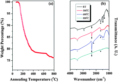 | ||
| Fig. 4 Results of (a) TGA and (b) FTIR analysis on the colloidal suspension of CNO− nanosheets annealed at various temperatures. | ||
Fig. 5(a) shows an SEM image of the CNO film deposited on a Pt–Si substrate at RT and subsequently annealed at 600 °C. A 112 nm-thick CNO film was well formed with a relatively sharp interface between the Pt electrode and the CNO film. A high resolution transmission electron microscopy (HRTEM) image of the CNO film annealed at 600 °C was also taken, as shown in Fig. 5(b). The fast Fourier transform (FFT) pattern obtained from the HRTEM image of the CNO film is shown in the inset of Fig. 5(b). The (001) lattice image is clearly shown in the HRTEM image of the CNO film and the FFT pattern showed the (001) peaks, indicating that the crystalline CNO film was well developed on the Pt electrode using the electrophoresis method.
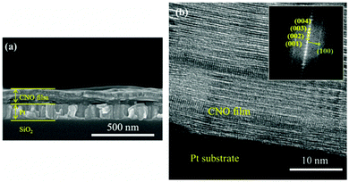 | ||
| Fig. 5 (a) SEM image and (b) HRTEM image of a CNO film deposited on a Pt–Si substrate at RT and subsequently annealed at 600 °C. The inset shows the FFT pattern obtained from the HRTEM image. | ||
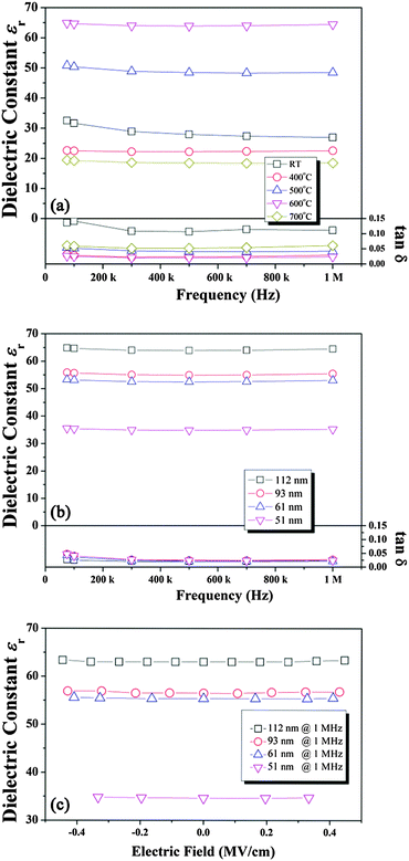
The εr and tan![[thin space (1/6-em)]](https://www.rsc.org/images/entities/char_2009.gif) δ values of the CNO films deposited at RT and subsequently annealed at various temperatures were measured at various frequencies, as shown in Fig. 6(a). The εr value of the film grown at RT was approximately 32 at 75 kHz and slightly decreased with increasing frequency to 29 at 1.0 MHz. However, it showed a large tan
δ values of the CNO films deposited at RT and subsequently annealed at various temperatures were measured at various frequencies, as shown in Fig. 6(a). The εr value of the film grown at RT was approximately 32 at 75 kHz and slightly decreased with increasing frequency to 29 at 1.0 MHz. However, it showed a large tan![[thin space (1/6-em)]](https://www.rsc.org/images/entities/char_2009.gif) δ value (>0.1) probably owing to the presence of a large amount of organic defects. For the film annealed at 400 °C, a slightly decreased εr value of 22 was observed with a small tan
δ value (>0.1) probably owing to the presence of a large amount of organic defects. For the film annealed at 400 °C, a slightly decreased εr value of 22 was observed with a small tan![[thin space (1/6-em)]](https://www.rsc.org/images/entities/char_2009.gif) δ value of 0.02 and their variation with respect to frequency was negligible. Since the film grown at 400 °C shows a small tan
δ value of 0.02 and their variation with respect to frequency was negligible. Since the film grown at 400 °C shows a small tan![[thin space (1/6-em)]](https://www.rsc.org/images/entities/char_2009.gif) δ value, the amount of defects that existed in this CNO film could be small. It is worth mentioning that the CNO film deposited at RT contains many defects such as TBA+ and H2O (or H3O+) and the εr value obtained from this film contains the effects of these defects, indicating that this εr value cannot be the εr of the pure CNO film. In addition, this film shows a large tan
δ value, the amount of defects that existed in this CNO film could be small. It is worth mentioning that the CNO film deposited at RT contains many defects such as TBA+ and H2O (or H3O+) and the εr value obtained from this film contains the effects of these defects, indicating that this εr value cannot be the εr of the pure CNO film. In addition, this film shows a large tan![[thin space (1/6-em)]](https://www.rsc.org/images/entities/char_2009.gif) δ value (>0.1), indicating that the defects considerably influenced the εr value of the CNO film grown at RT. In contrast, the films grown at high temperatures (≥400 °C) exhibit a small tan
δ value (>0.1), indicating that the defects considerably influenced the εr value of the CNO film grown at RT. In contrast, the films grown at high temperatures (≥400 °C) exhibit a small tan![[thin space (1/6-em)]](https://www.rsc.org/images/entities/char_2009.gif) δ value (<0.05) and the effect of the defects on the εr values of these films can be negligible, indicating that the εr value obtained from these films can be that of the pure CNO film. Therefore, the εr value obtained from the CNO film grown at RT cannot be compared with that of the films grown at high temperatures. Moreover, the εr value obtained from the film deposited at RT is higher than that of the film annealed at 400 °C because this CNO film contains many defects. The εr value of the CNO film increased considerably to 50 for the film annealed at 500 °C with a small tan
δ value (<0.05) and the effect of the defects on the εr values of these films can be negligible, indicating that the εr value obtained from these films can be that of the pure CNO film. Therefore, the εr value obtained from the CNO film grown at RT cannot be compared with that of the films grown at high temperatures. Moreover, the εr value obtained from the film deposited at RT is higher than that of the film annealed at 400 °C because this CNO film contains many defects. The εr value of the CNO film increased considerably to 50 for the film annealed at 500 °C with a small tan![[thin space (1/6-em)]](https://www.rsc.org/images/entities/char_2009.gif) δ of 0.03. Moreover, the maximum εr value of 65 with a very low tan
δ of 0.03. Moreover, the maximum εr value of 65 with a very low tan![[thin space (1/6-em)]](https://www.rsc.org/images/entities/char_2009.gif) δ of 0.01 was observed for the CNO film annealed at 600 °C. The increase of the εr value with the increase of annealing temperature could be due to the improved crystallinity of the film. However, for the film annealed at 700 °C, the εr value decreased to 20 with a slightly increased tan
δ of 0.01 was observed for the CNO film annealed at 600 °C. The increase of the εr value with the increase of annealing temperature could be due to the improved crystallinity of the film. However, for the film annealed at 700 °C, the εr value decreased to 20 with a slightly increased tan![[thin space (1/6-em)]](https://www.rsc.org/images/entities/char_2009.gif) δ of 0.05 at 1.0 MHz. This result could be due to the formation of a CaNb2O6 secondary phase. According to previous work, the εr value of the CNO film grown by the LB method was approximately 210 with a low tan
δ of 0.05 at 1.0 MHz. This result could be due to the formation of a CaNb2O6 secondary phase. According to previous work, the εr value of the CNO film grown by the LB method was approximately 210 with a low tan![[thin space (1/6-em)]](https://www.rsc.org/images/entities/char_2009.gif) δ of 0.01, which is higher than that of the CNO film grown by the electrophoresis method in this work.21 The film grown by the LB method was close to a single crystal film, and hence it showed a high εr value of 210.21 Therefore, if the crystallinity of the CNO film grown by the electrophoresis method increased by controlling the process conditions, it may also be possible to grow a CNO film with a larger εr value. The εr and tan
δ of 0.01, which is higher than that of the CNO film grown by the electrophoresis method in this work.21 The film grown by the LB method was close to a single crystal film, and hence it showed a high εr value of 210.21 Therefore, if the crystallinity of the CNO film grown by the electrophoresis method increased by controlling the process conditions, it may also be possible to grow a CNO film with a larger εr value. The εr and tan![[thin space (1/6-em)]](https://www.rsc.org/images/entities/char_2009.gif) δ values of the CNO films with various thicknesses annealed at 600 °C for 30 min are shown in Fig. 6(b). The εr value of the 112 nm-thick CNO film was approximately 65 and it decreased to 56 and 54 for the 93 nm-thick and 61 nm-thick CNO films, respectively. For the 51 nm-thick film, it was approximately 35. Moreover, all films showed low tan
δ values of the CNO films with various thicknesses annealed at 600 °C for 30 min are shown in Fig. 6(b). The εr value of the 112 nm-thick CNO film was approximately 65 and it decreased to 56 and 54 for the 93 nm-thick and 61 nm-thick CNO films, respectively. For the 51 nm-thick film, it was approximately 35. Moreover, all films showed low tan![[thin space (1/6-em)]](https://www.rsc.org/images/entities/char_2009.gif) δ values (<0.05 at 100 kHz). Therefore, the εr value of the CNO film decreased with decreasing film thickness. For the CNO film grown by the LB method, the decrease of the εr value with decreasing film thickness was not observed, and it was explained by the absence of a dead layer between the CNO film and the electrode.9–12 However, for the CNO film grown by the electrophoretic method, the εr value decreased with decreasing film thickness, suggesting that a dead layer existed between the CNO film and the Pt electrode. Moreover, the effect of the dead layer increased with decreasing CNO film thickness resulting in the smaller εr value for the thinner CNO film. Fig. 6(c) shows the variation of the εr value with respect to the applied electric field for the CNO films with various thicknesses. All films showed a constant εr value, although the applied electric field increased, indicating that the variation of the εr value with respect to the electric field is negligible.
δ values (<0.05 at 100 kHz). Therefore, the εr value of the CNO film decreased with decreasing film thickness. For the CNO film grown by the LB method, the decrease of the εr value with decreasing film thickness was not observed, and it was explained by the absence of a dead layer between the CNO film and the electrode.9–12 However, for the CNO film grown by the electrophoretic method, the εr value decreased with decreasing film thickness, suggesting that a dead layer existed between the CNO film and the Pt electrode. Moreover, the effect of the dead layer increased with decreasing CNO film thickness resulting in the smaller εr value for the thinner CNO film. Fig. 6(c) shows the variation of the εr value with respect to the applied electric field for the CNO films with various thicknesses. All films showed a constant εr value, although the applied electric field increased, indicating that the variation of the εr value with respect to the electric field is negligible.
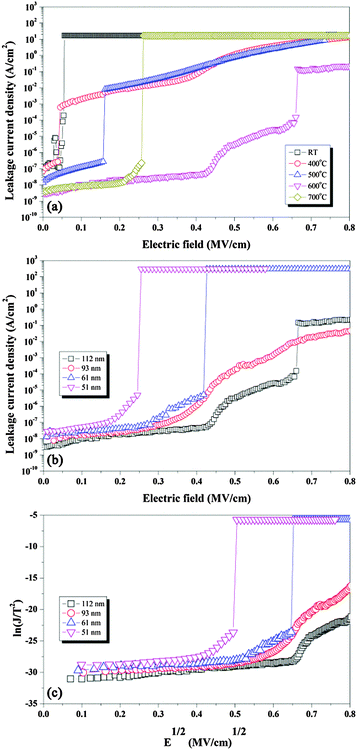
Fig. 7(a) shows the I–V characteristics of CNO films deposited at RT and annealed at various temperatures. The CNO film deposited at RT showed a reduced breakdown electric field of 0.05 MV cm−1, probably owing to the presence of defects in the film. Similar results were observed as well for films annealed at low temperatures (≤400 °C), indicating that the films annealed at temperatures below 500 °C contained organic defects, which degraded the electrical properties of the CNO film. The breakdown electric field increased for films annealed at temperatures higher than 400 °C, and a maximum breakdown electric field of 0.43 MV cm−1 was obtained for the CNO film annealed at 600 °C. This film also showed a very low leakage current density of 3 × 10⁻⁸ A cm−2 at 0.4 MV cm−1. However, for the film annealed at 700 °C, the breakdown electrical field was reduced to 0.22 MV cm−1 with a low leakage current density of 0.5 × 10⁻⁸ A cm−2 at 0.2 MV cm−1, probably owing to the formation of a CaNb2O6 secondary phase. Therefore, the CNO film deposited by the electrophoresis method at RT and subsequently annealed at 600 °C showed good dielectric and electric properties.
The I–V characteristics of the CNO films with different thicknesses annealed at 600 °C for 30 min were measured as shown in Fig. 7(b). All films show similar low leakage current densities at a low electric field of approximately <0.17 MV cm−1. Fig. 7(c) shows the ln(J/T2) vs. E1/2 curves for all CNO films, where J is current density and T is temperature. All films show a linear relation between ln(J/T2) and E1/2 below 0.4 (MV cm−1)1/2. Moreover, the index of refraction of all films calculated from the slope of ln(J/T2) vs. E1/2 curves (2.75) is very similar to the reported value (2.45).32 Therefore, the leakage current of all CNO films can be explained by Schottky emission,33,34 indicating that the leakage current density of the CNO film depends on the quality of the Pt/CNO interface, but the leakage current should not be influenced by the thickness of the film. Therefore, all films showed a similar leakage current density at low electric field, as shown in Fig. 7(b). However, each film had a different breakdown electric field; the thicker the film, the larger the breakdown electric field. Therefore, it can be suggested that the density of defects such as grain boundaries and voids might be higher in thinner films resulting in a lower breakdown electric field.
In addition, Fig. 8(a) and (b) show the SEM images of the surface of the CNO film annealed at 600 °C and 700 °C, respectively. A homogeneous surface was developed for the CNO film annealed at 600 °C. However, for the CNO film annealed at 700 °C, the CaNb2O6 secondary phase indicated by the arrows was formed along the grain boundaries of the film resulting in an inhomogeneous surface of the film. The insets in Fig. 8(a) and (b) show the AFM images of each CNO film. The root mean square value of the surface roughness (Rrms) of each CNO film is also shown in these figures. The Rrms value of the CNO film annealed at 600 °C is 12.1 nm and that of the CNO film annealed at 700 °C is approximately 34.5 nm. A very rough surface was formed for the CNO film annealed at 700 °C owing to the presence of the CaNb2O6 secondary phase that is shown in the SEM image. Therefore, the interface quality between the Pt top electrode and the CNO film annealed at 700 °C could be much worse than that formed in the CNO film annealed at 600 °C, leading to a larger leakage current density for the CNO film annealed at 700 °C. Therefore, the increase in the leakage current for the CNO film annealed at 700 °C can be also explained by the presence of the CaNb2O6 secondary phase.
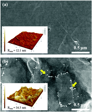 | ||
| Fig. 8 SEM images of the surface of CNO thin films annealed for 30 min at (a) 600 °C and (b) 700 °C. The inset of each figure shows the AFM image of the corresponding film. | ||
Conclusions
A colloidal suspension of CNO− nanosheets was well formed from a KCNO ceramic precursor through an exfoliation process. This CNO− colloid was used to deposit CNO films on a Pt–Si substrate by the electrophoresis method. The CNO film deposited at RT contained many organic defects. Most of the defects were removed for CNO films annealed at temperatures higher than 500 °C. However, a CaNb2O6 secondary phase formed for CNO films annealed at temperatures higher than 600 °C. A low εr value was obtained for CNO films annealed at temperatures below 500 °C. Moreover, CNO films annealed at temperatures below 500 °C showed a small breakdown electric field. The degraded dielectric and electric properties can be explained by the presence of organic defects in the CNO films. CNO films annealed above 600 °C also showed low dielectric and low electric properties due to the formation of a CaNb2O6 secondary phase. This result indicated that the optimum annealing temperature for growth of a CNO film is 600 °C. In particular, the CNO film annealed at 600 °C showed a high εr value of 65 with a low tan![[thin space (1/6-em)]](https://www.rsc.org/images/entities/char_2009.gif) δ of 0.01 at 1.0 MHz. It also exhibited a high breakdown electric field of 0.43 MV cm−1 and a very low leakage current density of 3 × 10⁻⁸ A cm−2 at 0.4 MV cm−1.
δ of 0.01 at 1.0 MHz. It also exhibited a high breakdown electric field of 0.43 MV cm−1 and a very low leakage current density of 3 × 10⁻⁸ A cm−2 at 0.4 MV cm−1.
Acknowledgements
This work was supported by the Industrial Strategic Technology Development Program, 10041232, “Development of synthesis method of exfoliated inorganic nanosheets with a high dielectric constant of >400 and the corresponding thin films applicable for the fabrication of high performance MLCC” funded by the Ministry of Knowledge Economy (MKE, Korea).References
- M. R. Joung, J. S. Kim, M. E. Song, J. H. Choi, S. Nahm, C. H. Choi and T. H. Sung, J. Alloys Compd., 2011, 509, 9089–9092 CrossRef CAS.
- M. R. Joung, I. T. Seo, J. S. Kim, J. H. Choi, S. Nahm, C. H. Choi and T. H. Sung, Jpn. J. Appl. Phys., 2011, 50, 035002 CrossRef.
- Y. Sakabe, J. Jpn. Soc. Powder Powder Metall., 2004, 51, 274–284 CrossRef.
- M. Dawber, K. M. Rabe and J. F. Scott, Rev. Mod. Phys., 2005, 77, 1083–1130 CrossRef CAS.
- C. S Hwang, S. O. Park, H. J. Cho, C. S. Kang, H. K. Kang, S. I. Lee and M. Y. Lee, Appl. Phys. Lett., 1995, 67, 2819–2821 CrossRef.
- K. Kukli, M. Ritala and M. Leskelä, J. Electrochem. Soc., 2001, 148, F35–F41 CrossRef CAS.
- G. D. Wilk, R. M. Wallace and J. M. Anthony, J. Appl. Phys., 2001, 89, 5243–5275 CrossRef CAS.
- M. Kadoshima, M. Hiratani, Y. Shimamoto, K. Torii, H. Miki, S. Kimura and T. Nabatame, Thin Solid Films, 2003, 424, 224–228 CrossRef CAS.
- C. Zhou and D. M. Newns, J. Appl. Phys., 1997, 82, 3081–3088 CrossRef CAS.
- K. Natori, D. Otani and N. Sano, Appl. Phys. Lett., 1998, 73, 632–634 CrossRef CAS.
- N. A. Pertsev, A. G. Zembilgotov and A. K. Tagantsev, Phys. Rev. Lett., 1998, 80, 1988–1991 CrossRef CAS.
- C. T. Black and J. J. Welser, IEEE Trans. Electron Devices, 1999, 46, 776–780 CrossRef CAS.
- S. W. Ko, T. Dechakupt, C. A. Randall, S. Trolier-McKinstry, M. Randall and A. Tajuddin, J. Electroceram., 2010, 24, 161–169 CrossRef CAS.
- R. E. Schaak and T. E. Mallouk, Chem. Mater., 2002, 14, 1455–1471 CrossRef CAS.
- R. E. Schaak and T. E. Mallouk, Chem. Mater., 2000, 12, 2513–2516 CrossRef CAS.
- J. Y. Kim, I. Chung, J. H. Choy and G. S. Park, Chem. Mater., 2001, 13, 2759–2761 CrossRef CAS.
- D. S. Kim, T. C. Ozawa, K. Fukuda, S. Ohshima, I. Nakai and T. Sasaki, Chem. Mater., 2011, 23, 2700–2702 CrossRef CAS.
- M. Osada, Y. Ebina, H. Funakubo, S. Yokoyama, T. Kiguchi, K. Takada and T. Sasaki, Adv. Mater., 2006, 18, 1023–1027 CrossRef CAS.
- K. Akatsuka, M. Haga, Y. Ebina, M. Osada, K. Fukuda and T. Sasaki, ACS Nano, 2009, 3, 1097–1106 CrossRef CAS PubMed.
- T. Tanaka, K. Fukuda, Y. Ebina, K. Takada and T. Sasaki, Adv. Mater., 2004, 16, 872–875 CrossRef CAS.
- M. Osada, K. Akatsuka, Y. Ebina, H. Funakubo, K. Ono, K. Takada and T. Sasaki, ACS Nano, 2010, 4, 5225–5232 CrossRef CAS PubMed.
- M. Osada, G. Takanashi, B. W. Li, K. Akatsuka, Y. Ebina, K. Ono, H. Funakubo, K. Takada and T. Sasaki, Adv. Funct. Mater., 2011, 21, 3482–3487 CrossRef CAS.
- W. Sugimoto, O. Terabayashi, Y. Murakami and Y. Takasu, J. Mater. Chem., 2002, 12, 3814–3818 RSC.
- M. Giersig and P. Mulvaney, Langmuir, 1993, 9, 3408–3413 CrossRef CAS.
- E. M. Wong and P. C. Searson, Chem. Mater., 1999, 11, 1959–1961 CrossRef CAS.
- Y. Matsumoto, A. Funatsu, D. Matsuo and U. Unal, J. Phys. Chem. B, 2001, 105, 10893–10899 CrossRef CAS.
- T. W. Kim, E. J. Oh, A. Y. Jee, S. T. Lim, D. H. Park, M. Y. Lee, S. H. Hyun, J. H. Choy and S. J. Hwang, Chem. – Eur. J., 2009, 15, 10752–10761 CrossRef CAS PubMed.
- S. H. Kweon, M. Im, G. Han, J. S. Kim, S. Nahm, J. W. Choi and S. J. Hwang, J. Eur. Ceram. Soc., 2013, 33, 907–911 CrossRef CAS.
- T. Sasaki, M. Watanabe, H. Hashizume, H. Yamada and H. Nakazawa, J. Am. Chem. Soc., 1996, 118, 8329–8335 CrossRef CAS.
- T. Sasaki, F. Kooli, M. Iida, Y. Michiue, S. Takenouchi, Y. Yajima, F. Izumi, B. C. Chakoumakos and M. Watanabe, Chem. Mater., 1998, 10, 4123–4128 CrossRef CAS.
- T. Sasaki and M. Watanabe, J. Am. Chem. Soc., 1998, 120, 4682–4689 CrossRef CAS.
- F. E. Osterloh, Comments Inorg. Chem., 2006, 27, 41–59 CrossRef CAS.
- Y. H. Kim, H. J. Kim, M. Osada, B. W. Li, Y. Ebina and T. Sasaki, ACS Appl. Mater. Interfaces, 2014, 6, 19510–19514 CAS.
- B. Y. Kim, T. G. Seong, I. T. Seo, J. S. Kim, C. Y. Kang, S. J. Yoon and S. Nahm, Acta Mater., 2012, 60, 7034–7040 CrossRef CAS.
| This journal is © The Royal Society of Chemistry 2016 |

