Low contact resistance in solid electrolyte-gated ZnO field-effect transistors with ferromagnetic contacts
Received
12th September 2015
, Accepted 23rd November 2015
First published on 24th November 2015
Abstract
Understanding the role of contacts and interfaces between ferromagnetic metals and semiconductors is a critical step for spin injection and transport. Here, high performance solid electrolyte gated ZnO field-effect-transistors (FETs) with ferromagnetic Co contacts as the source and drain electrodes were demonstrated. Solid electrolyte gating provides a large electric field in the FETs that leads to an ohmic contact between the Co electrode and the ZnO film. The contact resistance can be tuned by the gate voltage and reduced to 66 Ω cm. Compared with FETs using a traditional SiO2 dielectric, an improved transistor performance is achieved with a current on/off ratio of 106 and a field-effect mobility of 5.24 cm2 V−1 s−1. The magnetoresistance calculation based on a spin diffusion model indicates that the on-state contact resistance of the solid electrolyte gated FETs falls in the optimal range for the injection and detection of spin-polarized charge carriers. These results reveal that the electrolyte gating allows for engineering the contacts for nanoelectronic and spintronic devices.
Introduction
Spintronics, utilizing the spin of the electron for information storage and processing, holds great promise for the designing of novel next-generation electronic devices.1–8 The spin field-effect transistor (spin FET) proposed by Datta and Das is the most prominent proposal. The basic structure of spin FETs consists of a semiconductor channel between two ferromagnetic layers.9 So far, the low-efficiency spin injection from ferromagnetic contacts into semiconductors has remained an unsolved issue for realistic application of spin FETs.10,11 The realization of highly-efficient spin injection is impeded by several factors, such as resistance mismatch, Schottky barrier and non-tunneling transport.4 It is well known that the contacts and interfaces between metals and semiconductors play an important role.12–14 One of the conventional approaches widely used to overcome these problems is to insert a tunneling layer between the ferromagnetic contact and the semiconductor.14–16 Recently, Jen-Ru Chen et al. reported that a huge reduction of the Schottky barrier (from 60.6 meV to 9.7 meV) between the contact of ferromagnetic metal Co and single layer MoS2 can be achieved by inserting a 2 nm thick MgO tunneling layer.15 The Saroj Prasad Dash group obtained a similar result with 1 nm-thick TiO2 as the tunneling layer in two-dimensional material based FETs.16 Another method to reduce such a conductivity difference is to increase the doping concentration of the semiconductor. However, the induced spin relaxation originating from impurity scattering has a detrimental impact on carrier spin lifetime.5,17
An electric-double-layer (EDL) formed at a semiconductor/electrolyte interface provides a large electric field and this feature has attracted much attention.18–22 By using electrolytes, an EDL is formed after the ionic redistribution by applying an external electric field. The typical thickness of the EDL is only 1 nm, which can be regarded as a nanogap capacitor with a large specific capacitance exceeding ∼1 μF cm−2 and a high-density of carriers (1013 cm−2 ∼ 1015 cm−2) accumulated at the surface.23–25 Therefore, the EDL structure has been widely adopted to manipulate the physical properties of condensed matter, such as the insulator-to-metal transition,26 reversal of the magnetization27 and spin–orbit interaction.28–30 Furthermore, it was found that a very low contact resistance can be obtained in high-performance FETs by using EDL gate dielectrics.31–33
Transitional metal oxides exhibit rich physical properties which stem from the complex coupling between the charge, spin, orbital and lattice degrees of freedom in systems.34–36 The ZnO semiconductor has attracted great interest for spintronics and optoelectronic devices due to a long spin relaxation time and good optical and electrical properties.37 In this paper, we report on the fabrication of solid electrolyte-gated ZnO FETs with ferromagnetic Co contacts by using micrometer-sized carbon fibers as a mask. It is found that the solid electrolyte can greatly reduce the contact resistance and improve the transistor performance. We further calculate the magnetoresistance (MR) based on the spin diffusion model using the experimentally measured contact resistance. The MR results indicate that the solid electrolyte-gated systems hold great promise for spintronics.
Experimental procedures
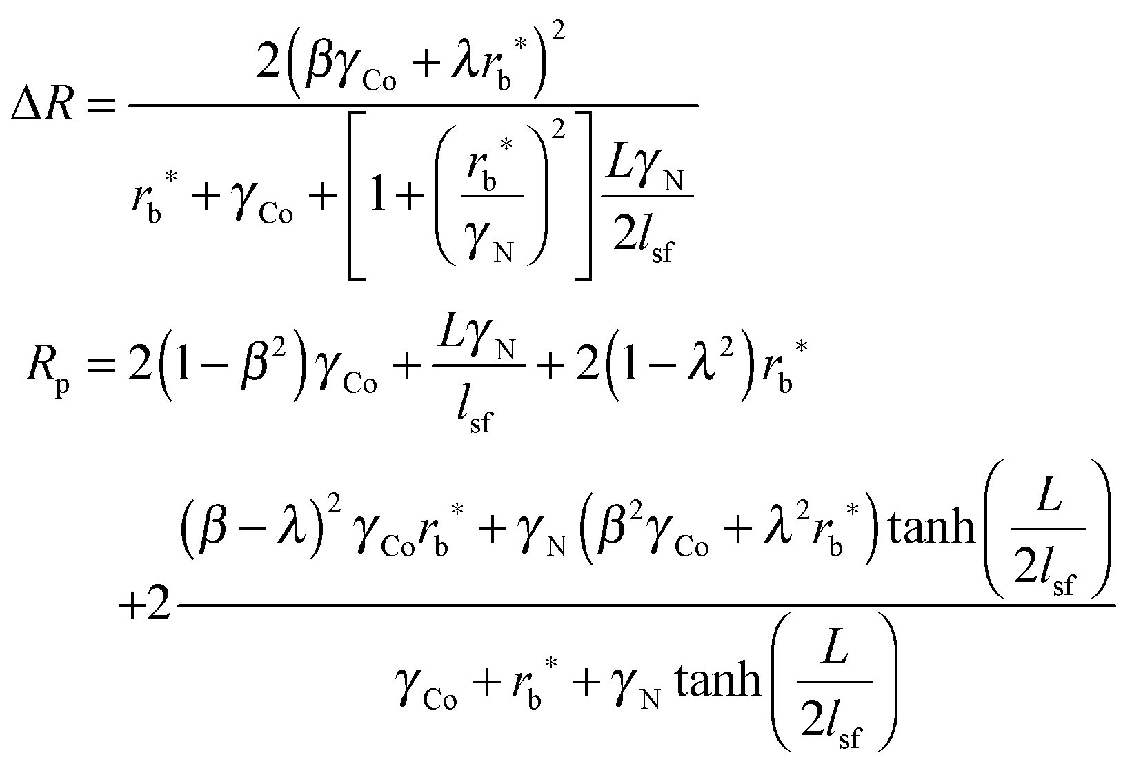
The indium-tin-oxide (ITO) glass substrates were ultrasonically cleaned in acetone, alcohol and distilled water for 15 min, and then dried by N2 flow and treated by ozone for 15 min. The 2 μm-thick SiO2 solid electrolyte was deposited on ITO as a gate dielectric.22 More details about the solid electrolyte can be found in our recent paper.38 A 15 nm-thick n-type ZnO thin film was deposited by RF magnetic sputtering as the active layer with a power of 30 W and a working pressure of 0.5 Pa at room temperature. Then, 10 μm-diameter carbon fibers were transferred onto the solid electrolyte/ITO substrates using tweezers (Fig. 1(a)). Generally, the carbon fiber adheres tightly to the surface by the electrostatic force of the device substrate. By using the 10 μm-diameter carbon fibers as the mask, the 40 nm-thick Co source–drain electrodes were deposited on ZnO by RF magnetic sputtering with a base vacuum of 8 × 10⁻⁵ Pa, a power of 80 W and a working pressure of 0.5 Pa. The deposition rate for the Co films is 0.63 Å s−1. The purity of the ZnO and Co targets is 99.99 wt%. Finally, the carbon fiber was slightly moved away from the substrate by tweezers. The channel width of the devices is 200 μm. The sputtered Co nanoclusters will diffract into the shadow regions of the carbon fiber; therefore, the actual channel length of the devices is less than 10 μm (Fig. 1(b)). Because the carbon fiber was not uniformly adhered to the substrate, a series of channels with different lengths were obtained between the Co source and the drain electrodes. The length of the channels for our devices was observed by a high resolution optical microscope. As shown in the graph in Fig. 1(c), the channel lengths varied from 1.7 μm to 5.2 μm. It is convenient to analyze the relationship between the channel length and the contact resistance described later. In order to compare the performance of the solid electrolyte-gated devices, thermally grown 200 nm-thick-SiO2/Si was also used for the fabrication of FETs. The resistivity and carrier density of ZnO were measured by Hall effects (Ecopia HMS-3000) with a Hall-bar structure. The electrical properties of the devices were measured by a Keithley 4200 semiconductor parameter analyzer in air and at room temperature.
 |
| | Fig. 1 ZnO FET with ferromagnetic contacts. (a) Fabrication of the ZnO FET with carbon fibers as a mask. (b) The schematic and the measurement configuration of the FET. (c) Optical microscope image of the channels of the FET. | |
Results and conclusions
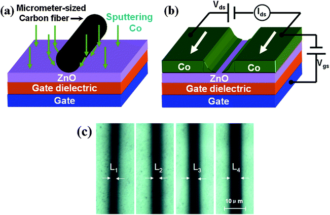
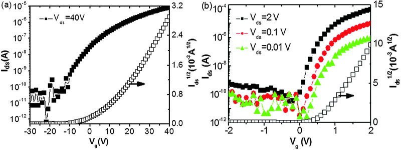
Low contact resistance is an important prerequisite to realize highly-efficient spin injection for spin FETs.15 We tested two types of devices: in one type, the 200 nm thermally grown SiO2 is used as the gate insulator and in the other the SiO2 solid electrolyte acts as the gate insulator. In both cases, the FETs have the same device dimensions (w/l = 200 μm/3.7 μm) and the sputtered ZnO channel was deposited under the same experimental conditions. Fig. 2(a) and (b) show the output characteristic curves of the drain–source current Idsversus the drain–source voltage Vds at different gate voltages Vg for the FET with traditional SiO2 and solid–electrolyte dielectrics, respectively. All of these devices exhibit n-type transistor properties, which is due to the Co Fermi level close to the conduction band of ZnO. Non-ohmic currents have been observed generally in the FETs with traditional dielectric layers and these devices exhibit a strong nonlinear Ids− Vds behavior. It suggests the presence of a high Schottky barrier and depletion of the carriers at the Co/ZnO contacts. In the low range of bias voltage, both types of devices show a linear Ids−Vds behavior (Fig. 2(c) and (d)); however, this feature is not a sufficient condition for a low-resistance ohmic contact.16 As demonstrated previously, the thermally assisted tunneling current can induce a linear behavior despite the presence of a high Schottky barrier, especially at a small bias voltage Vds.38 In contrast to the FETs with traditional dielectrics, a clear linear Ids−Vds characteristic was observed at low bias voltage in solid electrolyte-gated FETs, indicating the ohmic contact behavior of the Co pads directly on the ZnO layer as shown in Fig. 2(b). The Ids starts to saturate at higher Vds, which can be attributed to the channel pinch off. As shown in Fig. 2(d), the current at Vds = 0.5 V in the device with the solid electrolyte gate dielectric is achieved to be 12.7 μA for Vg = 2 V. However, the current at Vds = 0.5 V and Vg = 40 V for the FETs with 200 nm-thick thermally grown SiO2 is only 0.014 μA.
 |
| | Fig. 2 (a and b) Output Ids−Vds curves at different Vg values for the FET with traditional SiO2 and solid–electrolyte dielectrics, respectively. (c and d) Output curves at a low bias range at different Vg values for the FET with traditional SiO2 and solid–electrolyte dielectrics, respectively. | |
In order to exactly quantify the Co/ZnO contact resistance RC of the FETs, the transfer length method (TLM) was used. The Ids−Vds relationship of the fabricated FETs with a different channel length L was measured. The total resistance RT of different channel lengths at different Vg values can be calculated in a low Vds range. According to the TLM equation, the relationship between RT and RC can be given as:
| | 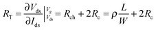 | (1) |
where
ρc is the sheet resistivity of the channel,
L is the channel length,
W is the channel width,
Rc is the resistance of one contact and
Rch is the resistance of the channel.
Fig. 3(a) shows the total resistance
RTversus L at different
Vg values (1 V, 1.5 V, 2 V) and linear fitting for each
Vg. The slope of the line is the resistivity
ρ and the
y-axis intercept is 2
RC. The slope decreases with increasing
Vg as expected for an n-type FET and the channel becomes more conductive. It can also be seen from
Fig. 3(a) that the contact resistance of the solid–electrolyte gated devices drops by 4.8 times as the
Vg increases from 1 V to 2 V. The contact resistance is as low as 66 Ω cm at
Vg = 2 V. As shown in
Fig. 3(b), the contact resistance of the FETs with 200 nm thermally grown SiO
2 is estimated to be 36.3 kΩ cm at
Vg = 40 V, which is 2–3 orders of magnitude higher than that of the FETs with a solid-electrolyte gate insulator at
Vg = 2 V. The reduction in the contact resistance with solid electrolyte gating is consistent with the
Ids−
Vds curve highlighted in
Fig. 2. It indicates that the total resistance of the solid electrolyte gated FETs is greatly reduced, which provides further evidence that the solid electrolyte gating can significantly reduce the contact resistance. A large contact resistance arises when the width of the Schottky barrier is large, which can prevent the tunneling process and further affect spin injection.
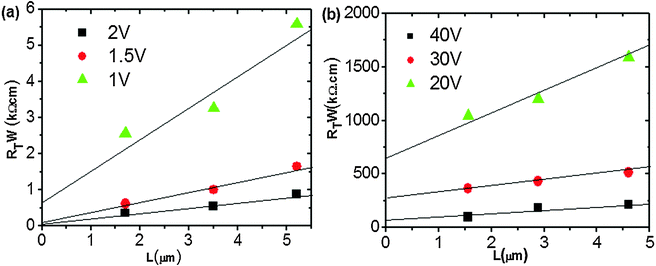 |
| | Fig. 3 Width normalized total (RT) and contact (RC) resistance of the FETs with a solid electrolyte (a) and 200 nm thermally grown SiO2 (b). | |
The decrease of contact resistance in the solid electrolyte gated FETs also results in an improved device performance. To compare the electrical performances of the two types of devices, transfer characteristics measurements (Idsvs. Vg) were performed at a variety of Vds values (Fig. 4). The mobility can be extracted from the saturation region slope of dIds1/2/dVG from the transfer characteristics:
| | 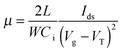 | (2) |
where
Ci is the gate capacitance (the
Ci of the solid electrolyte is about 1 μF cm
−2).
22 The devices with traditional SiO
2 exhibit an inferior performance with
μ = 0.023 cm
2 V
−1 s
−1 and the subthreshold swing is as high as 4.1 V per decade. The inferior device performance results from the weak gate coupling and the large Schottky barrier between the Co electrodes and the ZnO films. It can be found that the application of the solid electrolyte as an insulator layer shows a significant enhancement in the carrier mobility and the operating voltage is greatly reduced to 2 V. The mobility is found to be
μ = 5.24 cm
2 V
−1 s
−1 and the current on/off ratio is larger than 10
6. A threshold voltage (
VT) of 0.6 V and a subthreshold swing of 0.12 V per decade are also obtained. These results clearly indicate that the lower contact resistance in the metal/semiconductor interface is a necessary requirement for high performance devices.
16,31,32,39
 |
| | Fig. 4 (a) The transfer curves of the device with a traditional dielectric measured at a source–drain voltage of 40 V. (b) Transfer characteristics of the device with solid electrolyte gating at different source–drain voltages. | |
According to the basic theory of FETs, the width of the Schottky barrier can be calculated by the following formula:
| |  | (3) |
where
εZnO is the dielectric constant of the ZnO film (
εZnO = 8.75),
40εdielectric is the dielectric constant of the gate dielectric,
dZnO is the thickness of the ZnO film, and
ddielectric is the thickness of the gate dielectric. It means that for a 200 nm thick SiO
2 gate dielectric (the
εdielectric is 3.9), an electrical field of 2 MV cm
−1 was applied to the devices with
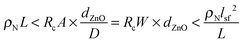
Vg = 40 V. Therefore, the calculated
λ = 82 nm is large enough for the direct charge tunneling and large contact resistance was observed. In contrast, the typical thickness of the EDL of the solid electrolyte (the
εdielectric is 2.2) is about 1 nm and there is an ultra-high electronic field of 20 MV cm
−1 applied on the FETs with solid electrolyte gating at
Vg = 2 V. The
λ can be calculated to be only ∼7.7 nm.
Fig. 5(a) is a sketch map of the band bending of the FETs at different electronic fields. Compared to the FET with traditional dielectrics, the reduction of the barrier width mainly results from a high density of charges accumulated in the solid electrolyte gated devices. Such strong coupling leads to the thinning of the barrier to several nanometers, which is essentially transparent for carriers and allows ohmic tunneling transport.
31,32,39 Furthermore, we also assess the viability of a lateral device structure for spintronic devices. For the solid electrolyte gated devices, the barrier width is reduced to several nanometers and the contact resistance is extremely small by applying a positive gate voltage. Thus, the spin-polarized carriers in ferromagnetic contacts can bypass the conductivity mismatch issues and tunnel through the thinned Schottky barrier into the channel. Therefore, a lateral FM/SC/FM structure can be considered as the lateral FM/I/SC/I/FM structure, where
I is the interface contact and FM is the ferromagnet. According to the spin diffusion theory, we estimated the MR (=Δ
R/
Rp) by putting the contact resistance into the formula
12| |  | (4) |
where Δ
R is the resistance difference between the antiparallel (
RAP) and parallel (
RP) configurations of the magnetizations of the two electrodes.
lsf is the spin diffusion length.
β and
γ are the bulk spin asymmetry coefficient in a Co electrode and the spin-dependent tunneling coefficient of the Co/ZnO/Co contact.
γN and
γCo are the product of
lsf and resistivity of the ZnO and Co, respectively. Considering the electrode length
D ≫
dZnO,
12 the interface resistance (
rb* =
RcA) should be within the range for high MR:
| |  | (5) |
where
Rc and
A are the product of the contact resistance and the contact area, respectively. By taking the experimentally measured carrier concentration and resistivity into account, we estimated the optimal range contact resistance for spin injection.
Fig. 5(b) displays the calculated MR as a function of gate voltage
Vg and contact resistance for the channel length of
L = 50 nm, and the expected spin lifetimes in ZnO are also indicated. Experimentally, the short channel (
L smaller than 50 nm) can be achieved by high-resolution electron-beam lithography. The shaded area between
Vg1 and
Vg2 predicts the possibility of observation with a significant change of MR in the Co–ZnO–Co device with solid electrolyte gating. The on-state contact resistance
RcA of the solid electrolyte gated FETs falls at the optimal range for the device with different spin lifetimes. In this paper, our aim is to prove that the spin injection from a ferromagnetic contact into a semiconductor would be realized by engineering the interface resistance. We are aware that extensive MR measurements are still needed. In our devices, the electric-double-layer effect of the solid electrolyte is generated by the assistance of water. So, the MR cannot be measured in a vacuum at low temperature. However, the method we used here was widely adopted by other groups and it is one of the most reasonable ways to calculate MR.
16,41–43 Although we have not fabricated a practical spin device in this process, the prediction of MR will give us a beneficial guidance in the future.
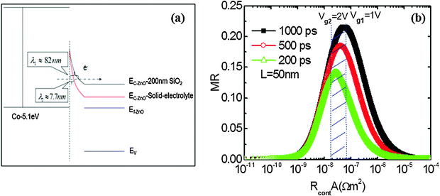 |
| | Fig. 5 (a) The band bending of the FETs at different electronic fields. (b) Calculated MR of the lateral FET structure as a function of the contact resistance and gate voltage with a channel length of 50 nm. | |
Conclusion
In conclusion, we demonstrated an improved FET performance using a solid electrolyte as the insulating layer with Co electrodes directly in contact on ZnO film. Comparing with the FETs with a traditional insulating layer, an improved device performance was observed with the mobility increased from 0.023 cm2 V−1 s−1 to 5.24 cm2 V−1 s−1 and the contact resistance decreased to 66 Ω cm. Furthermore, the contact resistance can be tuned by the gate voltage and the conductivity mismatch could be alleviated by solid electrolyte gating. The calculated magnetoresistance using a spin diffusion model indicates that the on-state contact resistance of the solid electrolyte gated FETs falls in the optimal range for injection and detection of spin-polarized charge carriers. The control of contact resistance encourages future studies of spintronic devices with electrolyte gating.
Acknowledgements
This work was supported by the National Natural Science Foundation of China (61306085, 51173205, 11334014, 11374373), the Doctoral Fund of the Ministry of Education of China (No. 20120162110020) and the support of China Postdoctoral Science Foundation (2015T80881). Y. G. acknowledges the support of National Science Foundation Grant No. DMR-1303742.
References
- X. Cartoixà, D. Z.-Y. Ting and Y.-C. Chang, Appl. Phys. Lett., 2003, 83, 1462 CrossRef.
- S. A. Wolf, D. D. Awschalom, R. A. Buhrman, J. M. Daughton, S. von Molnár, M. L. Roukes, A. Y. Chtchelkanova and D. M. Treger, Science, 2001, 294, 1488 CrossRef CAS PubMed.
- S. Sugahara and M. Tanaka, Appl. Phys. Lett., 2004, 84, 2307 CrossRef CAS.
- R. Jansen, S. P. Dash, S. Sharma and B. C. Min, Semicond. Sci. Technol., 2012, 27, 083001 CrossRef.
- J. Tang, C.-Y. Wang, L.-T. Chang, Y. Fan, T. Nie, M. Chan, W. Jiang, Y.-T. Chen, H.-J. Yang, H.-Y. Tuan, L.-J. Chen and K. L. Wang, Nano Lett., 2013, 13, 4036 CrossRef CAS PubMed.
- M. V. Kamalakar, A. Dankert, J. Bergsten, T. Lve and S. P. Dash, Sci. Rep., 2014, 4, 6146 CrossRef CAS PubMed.
- X.-J. Hao, T. Tu, G. Cao, C. Zhou, H.-O. Li, G.-C. Guo, W. Y. Fung, Z. Ji, G.-P. Guo and W. Lu, Nano Lett., 2010, 10, 2956 CrossRef CAS PubMed.
- M. Cinchetti, K. Heimer, J.-P. Wüstenberg, O. Andreyev, M. Bauer, S. Lach, C. Ziegler, Y. Gao and M. Aeschlimann, Nat. Mater., 2009, 8, 115 CrossRef CAS PubMed.
- S. Datta and B. Das, Appl. Phys. Lett., 1990, 56, 665 CrossRef CAS.
- P. Chuang, S.-C. Ho, L. W. Smith, F. Sfigakis, M. Pepper, C.-H. Chen, J.-C. Fan, J. P. Griffiths, I. Farrer, H. E. Beere, G. A. Jones, D. A. Ritchie and T.-M. Chen, Nat. Nanotechnol., 2015, 10, 35 CrossRef CAS PubMed.
- A. Fert, J.-M. George, H. Jaffrès and R. Mattana, IEEE Trans. Electron., 2007, 54, 921 CrossRef CAS.
- A. Fert and H. Jaffrès, Phys. Rev. B: Condens. Matter Mater. Phys., 2001, 64, 184420 CrossRef.
- G. Schmitdt, D. Ferrand, L. W. Molenkamp, A. T. Filip and B. J. van Wees, Phys. Rev. B: Condens. Matter Mater. Phys., 2000, 62, R4790 CrossRef.
- S. Heedt, C. Morgan, K. Weis, D. E. Bürgler, R. Calaco, H. Hardtdegen, D. Grutzmacher and T. Schäpers, Nano Lett., 2012, 12, 4437 CrossRef CAS PubMed.
- J.-R. Chen, P. M. Odenthal, A. G. Swartz, G. C. Floyd, H. Wen, K. Y. Luo and R. K. Kawakami, Nano Lett., 2013, 13, 3106 CrossRef CAS PubMed.
- A. Dankert, L. Langouche, M. V. Kamalakar and S. P. Dash, ACS Nano, 2014, 8, 476 CrossRef CAS PubMed.
- I. Žutić, J. Fabian and S. Das Sarma, Rev. Mod. Phys., 2004, 76, 323 CrossRef.
- Y. J. Zhang, T. Oka, R. Suzuki, J. T. Ye and Y. Iwasa, Science, 2014, 344, 725 CrossRef CAS PubMed.
- J. H. Cho, J. Lee, Y. Xia, B. Kim, Y. He, M. J. Renn, T. P. Lodge and C. D. Frisbie, Nat. Mater., 2008, 7, 900 CrossRef CAS PubMed.
- J. Schornbaum, Y. Zakharko, M. Held, S. Thiemann, F. Gannott and J. Zaumseil, Nano Lett., 2015, 15, 1822 CrossRef CAS PubMed.
- S. Fabiano, S. Braun, M. Fahlman, X. Crispin and M. Berggren, Adv. Funct. Mater., 2014, 24, 695 CrossRef CAS.
- J. Sun, Q. Wan, A. Lu and J. Jiang, Appl. Phys. Lett., 2009, 95, 222108 CrossRef.
- S. Ono, S. Seki, R. Hirahara, Y. Tominari and J. Takeya, Appl. Phys. Lett., 2008, 92, 103313 CrossRef.
- H. Yuan, H. Shimotani, A. Tsukazaki, A. Ohtomo, M. Kawasaki and Y. Iwasa, Adv. Funct. Mater., 2009, 19, 1046 CrossRef CAS.
- M. J. Panzer and C. D. Frisbie, Adv. Funct. Mater., 2006, 16, 1051 CrossRef CAS.
- H. Shimotani, H. Asanuma, A. Tsukazaki, A. Ohtomo, M. Kawasaki and Y. Iwasa, Appl. Phys. Lett., 2007, 91, 082106 CrossRef.
- Y. Yamada, K. Ueno, T. Fukumura, H. T. Yuan, H. Shimotani, Y. Iwasa, L. Gu, S. Tsukimoto, Y. Ikuhara and M. Kawasaki, Science, 2011, 332, 1065 CrossRef CAS PubMed.
- Z. Chen, H. Yuan, Y. Zhang, K. Nomura, T. Gao, Y. Gao, H. Shimotani, Z. Liu and Y. Iwasa, Nano Lett., 2012, 12, 2212 CrossRef CAS PubMed.
- S. Zhang, N. Tang, W. Jin, J. Duan, X. He, X. Rong, C. He, L. Zhang, X. Qin, L. Dai, Y. Chen, W. Ge and B. Shen, Nano Lett., 2015, 15, 1152 CrossRef CAS PubMed.
- C. Yin, H. Yuan, X. Wang, S. Liu, S. Zhang, N. Tang, F. Xu, Z. Chen, H. Shimotani, Y. Iwasa, Y. Chen, W. Ge and B. Shen, Nano Lett., 2013, 13, 2024 CrossRef CAS PubMed.
- J.-H. Choi, S. W. Lee, J. P. Kar, S. N. Das, J. Jeon, K.-J. Moon, T. I. Lee, U. Jeong and J.-M. Myoung, J. Mater. Chem., 2010, 20, 7393 RSC.
- I. Lokteva, S. Thiemann, F. Gannott and J. Zaumseil, Nanoscale, 2013, 5, 4230 RSC.
- D. Braga, M. Ha, W. Xie and C. D. Frisbie, Appl. Phys. Lett., 2010, 97, 193311 CrossRef.
- Y. Tian, S. R. Bakaul and T. Wu, Nanoscale, 2012, 4, 1529 RSC.
- Q. Wan, E. N. Dattoli, W. Y. Fung, W. Guo, Y. Chen, X. Pan and W. Lu, Nano Lett., 2006, 6, 2909 CrossRef CAS PubMed.
- Z. Zuo, H. Zhou, M. J. Olmedo, J. Kong, W. P. Beyermann, J.-G. Zheng, Y. Xin and J. Liu, J. Appl. Phys., 2012, 112, 053708 CrossRef.
- M. Opel, S. T. B. Goennenwein, M. Althammer, K.-W. Nielsen, E.-M. Karrer-Müller, S. Bauer, K. Senn, C. Schwark, C. Weier, G. Güntherodt, B. Beschoten and R. Cross, Phys. Status Solidi B, 2014, 251, 1700 CrossRef CAS.
- J. Sun, C. Qian, W. Huang, J. Yang and Y. Gao, Phys. Chem. Chem. Phys., 2014, 16, 7455 RSC.
- M. M. Perera, M.-W. Lin, H.-J. Chuang, B. P. Chamlagain, C. Wang, X. Tan, M. M.-C. Cheng, D. Tománek and Z. Zhou, ACS Nano, 2013, 5, 4449 CrossRef PubMed.
- Y. Chen, D. M. Bagnall, H. Koh, K. Park, K. Hiraga, Z. Zhu and T. Yao, J. Appl. Phys., 1998, 84, 3912 CrossRef CAS.
- B.-C. Min, K. Motohashi, C. Lodder and R. Jansen, Nat. Mater., 2006, 5, 817 CrossRef CAS PubMed.
- E.-S. Liu, J. Nah, K. M. Varahramyan and E. Tutuc, Nano Lett., 2010, 10, 3297 CrossRef CAS PubMed.
- M. V. Kamalakar, B. N. Madhushankar, A. Dankert and S. P. Dash, Small, 2015, 11, 2209 CrossRef CAS PubMed.
|
| This journal is © The Royal Society of Chemistry 2016 |