
 Open Access Article
 This Open Access Article is licensed under a
 Creative Commons Attribution 3.0 Unported Licence
Organometal halide perovskite thin films and solar cells by vapor deposition
Luis K.
Ono†
,
Matthew R.
Leyden†
,
Shenghao
Wang
and
Yabing
Qi
*
Energy Materials and Surface Sciences Unit (EMSS), Okinawa Institute of Science and Technology Graduate University (OIST), 1919-1 Tancha, Onna-son, Okinawa 904-0495, Japan. E-mail: Yabing.Qi@OIST.jp
First published on 1st December 2015
Abstract
Organometal halide perovskites (OHPs) are currently under the spotlight as promising materials for new generation low-cost, high-efficiency solar cell technology. Within a few years of intensive research, the solar energy-to-electricity power conversion efficiency (PCE) based on OHP materials has rapidly increased to a level that is on par with that of even the best crystalline silicon solar cells. However, there is plenty of room for further improvements. In particular, the development of protocols to make such a technology applicable to industry is of paramount importance. Vapor based methods show particular potential in fabricating uniform semitransparent perovskite films across large areas. In this article, we review the recent progress of OHP thin-film fabrication based on vapor based deposition techniques. We discuss the instrumentation and specific features of each vapor-based method as well as its corresponding device performance. In the outlook, we outline the vapor deposition related topics that warrant further investigation.
 Luis K. Ono | Luis K. Ono is a staff scientist in Prof. Yabing Qi's Unit (Energy Materials and Surface Sciences Unit) at Okinawa Institute of Science and Technology Graduate University in Japan. He obtained his B.S. in Physics/Microelectronics in 2000 from the University of Säo Paulo, Brazil. Later he joined the Department of Nuclear Engineering in Kyoto University, Japan, and the University of Central Florida, USA, where he obtained his M.S. in 2003 and Ph.D. in 2009, respectively. His current research focuses on the fundamental understanding of perovskite solar cells. |
 Matthew R. Leyden | Matthew Leyden received his Bachelor of Science in physics from Cal Poly San Luis Obispo in 2005, and then went on to receive his Ph.D. in physics from Oregon State University in 2011. He currently works as a postdoctoral scholar in Prof. Yabing Qi's Unit at Okinawa Institute of Science and Technology Graduate University researching perovskite synthesis by chemical vapor deposition. |
 Shenghao Wang | Shenghao Wang received his Master's degree in Condensed Matter Physics from Sichuan University, China and Doctor's degree in Applied Physics from University of Tsukuba, Japan, in 2010 and 2013, respectively. After that, he worked as a postdoctoral researcher in Akimoto Laboratory in University of Tsukuba. Currently he is a postdoctoral scholar in Prof. Yabing Qi's Unit (Energy Materials and Surface Sciences Unit) at Okinawa Institute of Science and Technology Graduate University (OIST). His research interests include surface and interface sciences, photoemission spectroscopy techniques, organic solar cells, and organic–inorganic hybrid perovskite solar cells. |
 Yabing Qi | Yabing Qi is currently an Assistant Professor and Head of Energy Materials and Surface Sciences Unit (EMSS) in Okinawa Institute of Science and Technology Graduate University (OIST). Dr Qi received his B.S., M.Phil., and Ph.D. degrees from Nanjing University, Hong Kong University of Science and Technology, and University of California Berkeley, respectively. His research interests include perovskite solar cells, organic electronics, surface sciences, energy materials and devices. Dr Qi has co-authored ∼50 peer-refereed papers and has delivered 70+ invited and contributed research presentations at international conferences, technical meetings and universities. |
1. Introduction
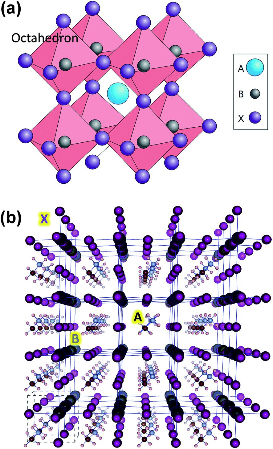
Organometal halide perovskite (OHP) solar cells have emerged as the most promising candidate for the next generation high efficiency solar cell technology that is compatible with low-cost, low-temperature processing, flexible substrates, and large-area fabrication using e.g. ultrasonic spray-coating,1 printing,2 roll-to-roll,3 and vapor deposition techniques.4,5 Laboratory scale cells with the highest power conversion efficiency (PCE) of ∼20.1% were achieved in a short time span of four years,6,7 which is only a few percent lower than the best single crystalline silicon solar cells.The term perovskite refers to a category of materials that can be represented by the building block of ABX3 and adopt a similar crystal structure to oxide perovskites such as calcium titanate (CaTiO3). A few review papers have been published on oxide and halide based perovskites with emphasis on solar cell application.8–20 In the particular case of OHPs, the halide anions (X = I, Br, or Cl) and metal cations (B = Pb, Sn) form the BX6 octahedral arrangement, Fig. 1a. The BX6 octahedra extend to a three-dimensional network in which cations A can be stabilized within the space formed by the eight adjacent octahedra (Fig. 1).21 The larger cation A (A being larger than B) can be Cs+,22 methylammonium (CH3NH3+, MA+), ethylammonium (CH3CH2NH3+, EA+),15 formamidinium (NH2CH![[double bond, length as m-dash]](https://www.rsc.org/images/entities/char_e001.gif) NH2+, FA+),23 or mixed CH3NH3 and 5-aminovaleric acid (5-AVA) cations [(5-AVA)x(CH3NH3)1−x].2 The crystallographic stability and probable structure are estimated by considering the Goldschmidt tolerance factor and the octahedral factor.9,15,16,24 Nevertheless, the determination of chemical and thermal stability of the resultant perovskite structure requires more detailed analysis.10 CH3NH3PbI3, the most commonly employed material in OHP solar cells, was reported to have a high absorption coefficient (direct bandgap of ∼1.55 eV) and high mobilities for electrons (7.5 cm2 V−1 s−1) and holes (12.5–66 cm2 V−1 s−1), i.e. ambipolar nature, resulting in long carrier diffusion lengths (100 nm to 1 μm).25 Although the amount and role of incorporated Cl are still under debate,26 mixed methylammonium-lead halide CH3NH3PbI3−xClx is another type of halide perovskite reported with an even higher charge-carrier mobility (∼33 cm2 V−1 s−1), resulting in carrier diffusion lengths of up to 3 μm.27 Theoretical studies have shown that most point defects in OHP form shallow defect states.28–32 In addition, grain boundaries were shown that they do not generate gap states, which makes the electronic property behavior of polycrystalline halide perovskite similar to that of a thin-film single crystal.28,29,33 In a recent work by deQuilettes et al.,34 the existence of large spatial variations in photoluminescence (PL) intensity and carrier recombination lifetimes were probed using a confocal PL microscope. In particular, higher contrasts were observed at the grain boundaries in comparison to the bulk of the material within the individual grains of CH3NH3PbI3−xClx perovskites.34 Differences in PL intensities were attributed to the variations in radiative and nonradiative recombination dynamics.34 The question whether the perovskite solar cell system is excitonic, similar to an organic solar cell, which requires a heterojunction interface to separate electron–hole pairs, or instead photoexcitations spontaneously dissociate into free carriers in the bulk, similar to inorganic solar cells, has not been completely settled.35–39 On the other hand, a number of studies suggest that exciton binding energies (BEs) in perovskites are in the range of ∼2–50 meV,35 and ultrafast interfacial charge-transfer dynamics take place;36 collectively, the majority of these observations imply that perovskite solar cells are predominantly non-excitonic similar to inorganic solar cells showing relatively low exciton BEs, e.g., Si (15.0 meV), GaAs (4.2 meV), and CdTe, (10.5 meV).37
NH2+, FA+),23 or mixed CH3NH3 and 5-aminovaleric acid (5-AVA) cations [(5-AVA)x(CH3NH3)1−x].2 The crystallographic stability and probable structure are estimated by considering the Goldschmidt tolerance factor and the octahedral factor.9,15,16,24 Nevertheless, the determination of chemical and thermal stability of the resultant perovskite structure requires more detailed analysis.10 CH3NH3PbI3, the most commonly employed material in OHP solar cells, was reported to have a high absorption coefficient (direct bandgap of ∼1.55 eV) and high mobilities for electrons (7.5 cm2 V−1 s−1) and holes (12.5–66 cm2 V−1 s−1), i.e. ambipolar nature, resulting in long carrier diffusion lengths (100 nm to 1 μm).25 Although the amount and role of incorporated Cl are still under debate,26 mixed methylammonium-lead halide CH3NH3PbI3−xClx is another type of halide perovskite reported with an even higher charge-carrier mobility (∼33 cm2 V−1 s−1), resulting in carrier diffusion lengths of up to 3 μm.27 Theoretical studies have shown that most point defects in OHP form shallow defect states.28–32 In addition, grain boundaries were shown that they do not generate gap states, which makes the electronic property behavior of polycrystalline halide perovskite similar to that of a thin-film single crystal.28,29,33 In a recent work by deQuilettes et al.,34 the existence of large spatial variations in photoluminescence (PL) intensity and carrier recombination lifetimes were probed using a confocal PL microscope. In particular, higher contrasts were observed at the grain boundaries in comparison to the bulk of the material within the individual grains of CH3NH3PbI3−xClx perovskites.34 Differences in PL intensities were attributed to the variations in radiative and nonradiative recombination dynamics.34 The question whether the perovskite solar cell system is excitonic, similar to an organic solar cell, which requires a heterojunction interface to separate electron–hole pairs, or instead photoexcitations spontaneously dissociate into free carriers in the bulk, similar to inorganic solar cells, has not been completely settled.35–39 On the other hand, a number of studies suggest that exciton binding energies (BEs) in perovskites are in the range of ∼2–50 meV,35 and ultrafast interfacial charge-transfer dynamics take place;36 collectively, the majority of these observations imply that perovskite solar cells are predominantly non-excitonic similar to inorganic solar cells showing relatively low exciton BEs, e.g., Si (15.0 meV), GaAs (4.2 meV), and CdTe, (10.5 meV).37
 | ||
| Fig. 1 (a) Ideal cubic perovskite structure with B metals assembled around X anions to form BX6 octahedron. A cation fills the space formed by the eight adjacent octahedra and balances the charge of the whole network. Reprinted with permission from Macmillian Publishers Ltd: Nature Photonics (ref. 15), copyright (2014). (b) Optimized structure for (pseudo)-cubic CH3NH3PbI3 with 4 × 4 × 4 supercell. Color coding: large dark gray: lead; purple: iodine; brown: carbon; small light gray: nitrogen; white: hydrogen atoms. Reprinted with permission from ref. 21. Copyright (2013) American Chemical Society. | ||
In the 1990s, Mitzi and co-workers studied OHPs and discovered desirable physico-chemical properties of these materials mainly for electronic applications.40–42 Almost in parallel, Grätzel and co-workers developed a new class of photovoltaic technology, dye-sensitized solar cells (DSSCs or Grätzel cell) and solid-state DSSCs (ssDSSCs) shown in Fig. 2.14,43,44 Miyasaka and co-workers were the first to apply perovskites in DSSCs in 2009.45 The dye was replaced by methylammonium lead triiodide/tribromide (CH3NH3PbI3 and CH3NH3PbBr3) perovskites in DSSC configuration13,14 obtaining a PCE of ∼3.8% and ∼3.1%, respectively, using the iodine/triiodide redox liquid electrolyte as the hole-transport material. Due to the high instabilities of the perovskite materials in the electrolytes, ruthenium-based dyes were still the preferable choice. In 2012, Park and co-workers fabricated all solid-state perovskite (CH3NH3PbI3) solar cells and achieved a PCE of ∼9.7% and much better durability.46 The key advance was made possible by replacing the liquid electrolyte with a solid hole transporting layer (HTL) material, Fig. 2.46 Since then, a myriad of reports have been published exploring the different perovskite materials, various device architectures, and fabrication methods.14,47–50 Both the dye and CH3NH3PbI3 assume the function of a sensitizer in which light absorption induces subsequent electron injection into the conduction band of the mesoporous TiO2 scaffold (electron transport layer, ETL) accompanied by hole injection from the oxidized sensitizer to the highest-occupied molecular orbital (HOMO) of the HTL. Further charge transport of electron and hole through the external circuit completes the photovoltaic operation.8 The use of TiO2 and HTL as selective contacts ensures that photoexcited charge carriers (electrons and holes) are transported in opposite directions. In a separate experiment, Lee et al.47 showed that a mesoporous (mp-) scaffold made of Al2O3 instead of TiO2 generated a similar PCE even though Al2O3 is an insulating material. This paradigm has been rationalized by suggesting that perovskite itself is a good electron conductor; if so, no mp-TiO2 scaffold is necessary at all. This led to a much simpler planar-type device architecture, Fig. 2, and first confirmed by Liu et al.,4 who showed efficient (PCE ∼ 15.4%) CH3NH3PbI3−xClx based perovskite solar cells without employing any mesoporous metal oxide layer. Etgar et al.51 had demonstrated that CH3NH3PbI3 could also act as an efficient hole conductor, which could even eliminate the need for employing the additional HTL layer. However, generally both electron and hole selective contacts contribute to the enhancement of the cell fill factor (FF). In particular, the hole selective contact tends to enhance the open-circuit voltage (Voc) by minimizing interfacial charge recombination processes, i.e. the HTL performs both functions of blocking electrons as well as transporting holes efficiently.52
 | ||
| Fig. 2 Evolution of the solar cell technology starting from the electrolyte-based mesoscopic DSSC and solid state (ss) DSSC where the electrolyte is replaced with an organic p-type hole conductor. Structural evolution of perovskite-based solar cells evolved from (i) sensitized solar cell with nanodot perovskite; (ii) mesoporous (scaffold) structured solar cell with a thin and continuous layer of perovskite; (iii) perovskite-infiltrated solar cell with a capping layer of perovskite; (iv) thin film planar heterojunction perovskite solar cell. Adapted with permission from ref. 14. Copyright (2013) American Chemical Society. | ||
The film morphology, thickness, stoichiometry, crystallinity as well as material purity have significant impact on the overall solar cell performance. A variety of solution- and vapor-based OHP deposition techniques have been reported including one-step spin-coating,53–57 two-step deposition techniques,41,58–60 solvent–solvent extraction,61 vapor-assisted solution processes,62–69 dual-source vacuum deposition,4,5,70–77 hybrid deposition,78–81 hybrid chemical vapor deposition,82–87 sequential vapor deposition,88–92 flash evaporation,93etc. One-step spin-coating is one of the widely used methods because of its simplicity and low-cost. However, the films prepared by this method often have a poor morphology (incomplete coverage) especially in the case of planar architecture, which results in decreased solar cell performance.54,94–96 In the two-step process,41,58,59 a layer of metal halide is deposited by spin-coating followed by dipping the film into the organic salt solution and perovskite formed by a chemical reaction. However, due to the high reaction rates of perovskite formation, it is challenging to optimize the processing conditions with sufficient reproducibility.97 Despite the fact that laboratory record efficiencies have been obtained by solution processing,7,50,98 it is observed that the reaction kinetics need to be rigorously controlled to maintain consistent device performance and minimize batch-to-batch variations.99 Yang and co-workers introduced a CH3NH3I vapor-based approach for the deposition of a perovskite layer called vapor-assisted solution process (VASP).62,63,65 In their process, PbI2 films were annealed in MAI vapor at 150 °C in an N2 environment for 2 h, Fig. 3a. Perovskite films exhibited high crystallinity, uniform surface coverage and large grain sizes up to 1 micrometer, Fig. 3b–d. The high quality films of CH3NH3PbI3 enabled enhanced solar cell parameters of short-circuit current (Jsc), Voc, FF, and PCE: 19.8 mA cm−2, 0.924 V, 0.663, 12.1%, respectively, in a planar architecture, Fig. 3e.62,63 The surface roughness of the films was measured by atomic force microscopy (AFM) (5 × 5 μm2, Fig. 3f) and calculated to be 23.2 nm. In a recent publication, the authors state that it is still unclear why the efficiency of perovskite solar cells based on VASP is slightly lower than that of devices derived from an optimized solution process.65 In this review, we focus on the different vapor-based methods to deposit perovskite films, which in many cases show properties different from their counterparts prepared by solution-based methods.
 | ||
| Fig. 3 (a) Schematic illustration of the vapor-assisted solution process (VASP). Perovskite film on the FTO/c-TiO2 substrate, obtained by reacting PbI2 film and CH3NH3I vapor at 150 °C for 2 h in an N2 atmosphere; (b) top-view SEM image (inset image with higher resolution, scale bar 1 μm); (c) XRD pattern; (d) cross-sectional SEM image; (e) J–V characteristics of CH3NH3PbI3 based solar cell generating efficiencies of 12.1% under AM1.5G illumination. Spiro-MeOTAD and Ag were used as the HTL and top electrode, respectively; (f) tapping-mode AFM height images (5 × 5 μm2) (inset: the corresponding 3D topographic image). The corresponding surface roughness of 23.2 nm was reported. Reprinted with permission from ref. 62. Copyright (2013) American Chemical Society. | ||
2. Vapor deposition by dual-source
2.1. Vapor deposition system description
Vapor deposition techniques are widely used in the semiconductor industry aiming at large scale production in optoelectronic applications. The viability of OHP material synthesis by physical vapor deposition techniques has also been demonstrated.4,5,70–74,100 Such techniques offer unique advantages such as (1) it is feasible to fabricate films with high-purity as the films are formed by sublimating the powder precursors after extensive outgassing under a vacuum environment; (2) in general, the initial nominal stoichiometry of precursors (e.g., CH3NH3I and PbCl2) can be well controlled in both solution and vacuum evaporation methods. On the other hand, it is necessary to take into account the solubility of precursors in determining the composition of the films that are prepared by solution methods. For example, it is difficult to dissolve PbCl2 in N,N-dimethylformamide (DMF) when the CH3NH3I![[thin space (1/6-em)]](https://www.rsc.org/images/entities/char_2009.gif) :PbCl2 molar ratio is lower than 3:1.47 (3) The commonly used solvents, in the solution process, can get intercalated in perovskite films. DMF, H2O, and dimethylsulfoxide (DMSO) were observed to form stable intermediate complexes of CH3NH3PbI3·DMF,101 CH3NH3PbI3·H2O,102 and CH3NH3PbI3·DMSO,103 respectively, likely to affect the perovskite film stability. (4) Vapor deposition techniques are suitable for the preparation of multilayered structures of thin films, while it is challenging for solution processing. (5) With proper optimization, perovskite films can be deposited by vapor deposition on a variety of substrates. The wettability issues in solution processing often lead to non-uniform coating and pin-hole formation.
:PbCl2 molar ratio is lower than 3:1.47 (3) The commonly used solvents, in the solution process, can get intercalated in perovskite films. DMF, H2O, and dimethylsulfoxide (DMSO) were observed to form stable intermediate complexes of CH3NH3PbI3·DMF,101 CH3NH3PbI3·H2O,102 and CH3NH3PbI3·DMSO,103 respectively, likely to affect the perovskite film stability. (4) Vapor deposition techniques are suitable for the preparation of multilayered structures of thin films, while it is challenging for solution processing. (5) With proper optimization, perovskite films can be deposited by vapor deposition on a variety of substrates. The wettability issues in solution processing often lead to non-uniform coating and pin-hole formation.
In 1997, Era et al.104 reported for the first time the dual-source vapor deposition method to form two-dimensional layered hybrid lead iodide intercalated with an organic ammonium layer. The synthesis of (RNH3)2PbI4 layered perovskite was performed under a pressure of ∼10−6 Torr sublimating PbI2 and organic ammonium iodide RNH3I (2-phenylethylammonium iodide C6H5C2H4NH3I was used as RNH3I). The synthesis of KPbI3 under vacuum from the PbI2 and KI precursor sources was reported by Salau.105 KPbI3 has been suggested as a potential candidate for solar cell applications because of its high thermal stability (220 °C).105
In 2013, Liu et al.4 reported the synthesis of three-dimensional CH3NH3PbI3−xClx by using the dual-source vapor deposition technique with PbCl2 and CH3NH3I as precursors leading to high efficiency photovoltaic devices (PCE ∼ 15.4%, Table 1). Similarly, Malinkiewicz et al. deposited a pure CH3NH3PbI3 perovskite by using PbI2 and CH3NH3I sources showing uniform film formation with a root mean square (RMS) roughness of 5 nm measured by AFM.5 In addition, the films showed uniform grainy structures with an average grain size of 150 nm.71 The schematic illustration of the dual-source vacuum deposition process is shown in Fig. 4.71,75 PbX2 (X = I, Cl) and CH3NH3I precursor materials contained in crucibles are heated (co-evaporation) to their corresponding sublimation temperatures. CH3NH3PbI3−xClx and CH3NH3PbI3 perovskites layers are formed on the substrate that is fixed at a distance of ∼20 cm above the crucibles.5 Typical base pressures of 10−5 to 10−6 Torr are reached after loading the precursor materials.4,5 The stoichiometry (chemical composition) and film thickness are monitored with the aid of piezo-electric sensors4,5 mounted inside the vacuum chamber (or a quartz crystal microbalance, QCM). Because perovskites are formed by the co-evaporation process, it requires the initial calibration as precise as possible for the thicknesses of individual evaporated PbX2 and CH3NH3I films. Material density (ρ), acoustic impedance (or Z-ratio), and geometric (or tooling factor) are parameters that need to be determined for the calibration of evaporation rate of the material being sublimated. Often it is difficult to find those parameters especially for organic compounds. For example, Liu et al. assumed the density and Z-ratio of CH3NH3I to be 1 g cm−3 and 1, respectively, because its precise density is unknown.4 The density for CH3NH3Cl of 1.1 g cm−3 was previously reported.4 More recently, the density value of 2.224 g cm−3 for CH3NH3I has been reported.80 In addition, the tetragonal CH3NH3PbI3 perovskite phase was calculated to have a density of 4.149 g cm−3.80 The densities of PbCl2 and PbI2 can be found in the literature with typical values of 5.85 g cm−3 and 6.16 g cm−3, respectively. As the source-to-substrate distance generally differs from the source-to-QCM distance, it is often a common practice to perform some initial tests to determine the tooling factor. A certain amount of material is deposited on a flat substrate recording the nominal thickness measured by the QCM with a preset tooling factor value. This nominal thickness value is then compared to the thickness value determined using another technique (e.g., AFM or surface profilometry). The linear relationship provides the new tooling factor of the evaporation system. As it will be discussed in more detail in the next section (3. Hybrid deposition method), the calibration procedure for the CH3NH3I was reported to be difficult due to the formation of a non-uniform layer dominated by the Volmer–Weber or Stranski–Krastanov growth mode and the volatile nature of the organic film.5,71,78,79 Alternatively Malinkiewicz et al.5,71 kept the evaporation temperature for the CH3NH3I crucible constant (at 70 °C) and varied the CH3NH3I:PbI2 ratio by changing only the evaporation temperature of the PbI2 crucible (250–260 °C). The optimum conditions were determined by analyzing the evaporated perovskite films by grazing incident X-ray diffraction (GIXRD). Once the optimum PbI2 crucible temperature (250 °C) for generating the stoichiometric perovskite is determined, perovskite films with similar properties can be prepared reproducibly indicating the robustness of the protocol.5,71
| Solar cell architecturea | Perovskite thickness (nm) | Electrode active area (cm2) | J sc (mA cm−2) | V oc (V) | FF | PCE (%) | Norm. PCE/thickness (×%/100 nm) | Ref. |
|---|---|---|---|---|---|---|---|---|
| a Abbreviations: FTO = fluorine doped tin oxide; c.l.-TiO2 = compact layered TiO2; spiro = 2,7′–7,7′-tetrakis-(N,N-di-p-methoxyphenylamine)-9,9′-spirobifluorene; ITO = indium tin oxide; PEDOT-PSS = poly(3,4-ethylenedioxy-thiophene):poly(styrene sulfonate); polyTPD = poly(N,N′-bis(4-butylphenyl)-N,N′-bis(phenyl)benzidine); PCBM = (6,6)-phenyl C61-butyric acid methyl ester; Bphen = bathophenanthroline; NPB = N,N′-di(1-naphthyl)-N,N′-diphenyl-(1,1′-biphenyl)-4,4′-diamine; BCP = bathocuproine; 3TPYMB = tris(2,4,6-trimethyl-3-(pyridine-3-yl)phenyl)borane; F6-TCNNQ = 2,2′-(perfluoronaphtalene-2,6-diylidine)dimalononitrile; spiro-MeO-TPD = 2,7-bis[N,N-bis(4-methoxy-phenyl)amino]-9,9-spirobifluorene; PCDTBT = poly(N-9′-heptadecanyl-1,2,7-carbazole-alt-5,5-(4′,7′-di(thien-2-yl)-2′1′,3′-benzothia-diazole)). b Not provided. | ||||||||
| FTO/c.l.-TiO2/CH3NH3PbI3−xClx/spiro/Ag (co-evaporation) | 330 | 0.076 | 21.5 | 1.07 | 0.68 | 15.4 | 4.7 | 4 |
| ITO/PEDOT:PSS/polyTPD/CH3NH3PbI3/PCBM/Au (co-evaporation) | 285 | 0.09 | 16.12 | 1.05 | 0.67–0.68 | 12.04 | 4.2 | 5 |
| 285 | 0.98 | 14.76 | 1.05 | 0.52 | 8.27 | 2.9 | ||
| ITO/PEDOT:PSS/polyTPD/CH3NH3PbI3/PCBM/Au (co-evaporation) | 285 | 0.06 | 18.8 | 1.07 | 0.63 | 12.7 | 4.5 | 70 |
| ITO/PEDOT:PSS/polyTPD/CH3NH3PbI3/PCBM/3TPYMB/Au (co-evaporation) | 285 | 0.065 | 18.2 | 1.09 | 0.75 | 14.8 | 5.2 | 71 |
| 285 | 0.95 | 17.9 | 1.07 | 0.57 | 10.9 | 3.8 | ||
| ITO/PEDOT:PSS/PCDTBT/CH3NH3PbI3/PC60BM/LiF/Ag (co-evaporation) | 370 | 0.2 | 21.9 | 1.05 | 0.72 | 16.5 | 4.5 | 37 |
| FTO/NiO/CH3NH3PbI3−xClx/PCBM/Ag (co-evaporation) | 250 | 0.07 | 14.2 | 0.786 | 0.65 | 7.26 | 2.9 | 72 |
| FTO/CuSCN/CH3NH3PbI3−xClx/PCBM/Ag (co-evaporation) | 500 | 0.07 | ∼8.8 | 0.677 | —b | 3.8 | 0.8 | 72 |
| ITO/F6-TCNNQ/spiro-MeO-TPD/CH3NH3PbI3−xClx/C60/Ag (co-evaporation) | 390 | 0.064 | 16.0 | 1.03 | 0.66 | 10.9 | 2.8 | 74 |
| ITO/MoO3/NPB/CH3NH3PbI3/C60/BCP/Al (co-evaporation) | 320 | 0.04 | 18.1 | 1.12 | 0.68 | 13.7 | 4.2 | 73 |
| ITO/CH3NH3PbI3−xClx/C60/Bphen/Al (co-evaporation) | 150 | 0.1 | 12.5 | 0.82 | 0.60 | 6.1 | 4.1 | 76 |
| FTO/PEDOT:PSS/CH3NH3PbI3−xClx/PCBM/Ag (co-evaporation) | 400 | 0.12 | 17.3 | 0.97 | 0.63 | 10.5 | 2.6 | 77 |
| FTO/c.l.-TiO2/CH3NH3PbI3−xClx/spiro/Ag (hybrid deposition) | 50 | 0.05 | 10.5 | 1.06 | 0.566 | 6.3 | 12.6 | 78 |
| 135 | 0.05 | 17.0 | 1.09 | 0.535 | 9.9 | 7.3 | ||
| FTO/c.l.-TiO2/CH3NH3PbI3/spiro/Au (hybrid deposition) | 170 | 0.05 | 19.92 | 1.098 | 0.524 | 11.48 | 6.8 | 79 |
| FTO/c.l.-TiO2/CH3NH3PbI3/spiro/Au (hybrid deposition) | 270–300 | 0.16 | ∼18 | >1.1 | >0.7 | >12 | >4.4 | 80 |
| FTO/C60/CH3NH3PbI3/spiro/Au (hybrid deposition) | 320 | 0.08 | 18.9 | 1.10 | 0.754 | 15.7 | 4.9 | 81 |
| FTO/C70/CH3NH3PbI3/spiro/Au (hybrid deposition) | 320 | 0.08 | 18.6 | 1.03 | 0.777 | 14.9 | 4.7 | |
| FTO/c.l.-TiO2/CH3NH3PbI3−xClx/spiro/Au (hybrid CVD) | 296 | 0.07–0.1 | 19.1 | 0.92 | 0.62 | 10.8 | 3.6 | 82 |
| FTO/c.l.-TiO2/HC(NH2)2PbI3−xClx/spiro/Au (hybrid CVD) | 324 | 0.04–0.169 | 20.9 | 1.03 | 0.66 | 14.2 | 4.4 | 83 |
| 324 | 1 | 18.4 | 0.97 | 0.43 | 7.7 | 2.4 | ||
| FTO/c.l.-TiO2/CH3NH3PbI3/spiro/Ag (low-pressure CVD) | —b | 0.12 | 21.7 | 0.91 | 0.65 | 12.73 | — | 85 |
| FTO/c.l.-TiO2/CH3NH3PbI3/spiro/Ag or Au (in situ tubular CVD) | 320 | 0.12 | 21.0 | 0.952 | 0.61 | 12.2 | 3.8 | 84 |
| ITO/PEDOT:PSS/CH3NH3PbI3−xClx/C60/Bphen/Ca/Ag (sequential deposition) | 430 | 0.05 | 20.9 | 1.02 | 0.722 | 15.4 | 3.6 | 88 |
| ITO/CH3NH3PbI3/C60/Ag (sequential deposition) | ∼350 | 0.09 | 13.6 | 0.8 | 0.5 | 5.4 | 1.5 | 89 |
| FTO/c.l.-TiO2/CH3NH3PbI3/spiro/MoO3/Al (sequential deposition) | 473 | 0.09 | 21.8 | 0.96 | 0.6 | 12.5 | 2.6 | 90 |
| FTO/c.l.-TiO2/CH3NH3PbI3/P3HT/Au (sequential deposition) | ∼400 | 0.104 | 21.76 | 0.96 | 0.653 | 13.7 | 3.4 | 91 |
| FTO/c.l.-TiO2/CH3NH3PbI3−xClx/spiro/Au (sequential deposition) | 412 | 0.071 | 22.27 | 1.00 | 0.72 | 16.03 | 3.9 | 92 |
| 0.49 | 20.91 | 0.98 | 0.69 | 14.14 | 3.4 | |||
| 1 | 20.77 | 0.98 | 0.68 | 13.84 | 3.4 | |||
| ITO/PEDOT:PSS/CH3NH3PbI3/polyTPD/PCBM/Ba/Ag (flash evaporation) | 200 | —b | 18 | 1.067 | 0.68 | 12.2 | 6.1 | 93 |
 | ||
| Fig. 4 Illustration of the dual-source vacuum deposition instrument. The PbX2 (X = I, Cl) and CH3NH3I (MAI) precursors are thermally evaporated in vacuum. The deposition rate and thickness are monitored using quartz microbalances. Reproduced with permission from ref. 75. | ||
The substrate holder is maintained at near room-temperature during perovskite deposition for the processes described above.4,5,71 Because of low-temperature processing, it is highlighted that the technique is of particular interest for the deposition of perovskite films onto flexible substrates. Liu et al.4 provide side-by-side comparison on the morphology of the CH3NH3PbI3−xClx perovskite films prepared by the solution and dual-source vacuum evaporated films. For example, the top- and side-views of scanning electron microscopy (SEM) highlight that vacuum-deposited films show full coverage and are extremely uniform with crystalline features on the size scale of hundreds of nanometers, Fig. 5a and b. Large-area cross-sectional SEM images, Fig. 5c and d, reveal that solution-processed films exhibit large variations in film thickness (50 to 410 nm) over the sample area, whilst vacuum-evaporated films have a constant film thickness of ∼330 nm. X-ray diffraction (XRD) patterns for both solution- and vacuum-processed show the main diffraction peak positions to be identical indicating that both techniques generate similar mixed-halide perovskite, Fig. 5e. The observed diffraction peaks at 14.12°, 28.44°, and 43.23° are assigned to the (110), (220), and (330) planes of the orthorhombic crystal structure.47 The small peak at 12.65° is assigned to the (110) diffraction peak of the remaining PbI2 compound. The best solar cell device based on the planar heterojunction architecture of FTO/c.l.-TiO2/CH3NH3PbI3−xClx/spiro-MeOTAD/Ag generates solar cell parameters of Jsc, Voc, FF, and PCE: 21.5 mA cm−2, 1.07 V, 0.67, 15.4%, respectively, Fig. 5f.
 | ||
| Fig. 5 (a) SEM top-view of vacuum-deposited CH3NH3PbI3−xClx perovskite film. (b) Cross-sectional SEM image under high magnification of the complete cell fabricated from vacuum-deposited perovskite film. (c and d) Cross-sectional SEM images under lower magnification comparing the (c) vacuum- and (d) solution-processed perovskite films. (e) XRD spectra of vacuum- and solution-processed perovskite films. J–V curves of the best performing vacuum- and solution-processed planar heterojunction perovskite solar cells measured under AM1.5 (101 mW cm−2) irradiance and in the dark. Reprinted with permission from Macmillan Publishers Ltd: Nature (ref. 4), copyright (2013). | ||
More recently, Lin et al.37 reported the use of vacuum-processed CH3NH3PbI3-perovskite planar structures with optimized ultrathin n- and p-type organic interlayers of PCBM and PCPDTBT, respectively, which serve to modify the electrode work functions. Enhanced solar cell parameters were obtained: Jsc = 21.9 mA cm−2, Voc = 1.05 V, FF = 0.72, and PCE = 16.5%. The complete devices (ITO/PEDOT:PSS/PCPDTBT/CH3NH3PbI3/PCBM/LiF/Ag) had an active area of 0.2 cm2.
2.2. Large-area solar cell
The first attempt for the fabrication of a larger-area solar cell (0.95 cm2) was reported by Malinkiewicz et al. in an inverted device architecture (ITO/PEDOT:PSS/polyTPD/CH3NH3PbI3/PCBM/3TPYMB/Au), Fig. 6. In most reports the active area sizes of the cells are smaller than 0.1 cm2, Table 1. Despite the general trend of lower FF as the active area increased, the authors observed that the high Voc was maintained and attributed to negligible surface and sub-bandgap trap states in vacuum-deposited perovskite films.5 The industrial-scale manufacturing of perovskite solar cells urgently calls for methods that are suitable to coat high-quality perovskite films over a large area (e.g. 1 cm2 or larger).15 | ||
| Fig. 6 J–V curves for the optimized CH3NH3PbI3 perovskite layer with a small (A = 0.065 cm2) and larger (A = 0.95 cm2) electrode size. The solar cell in planar heterojunction architecture is composed by ITO/PEDOT:PSS/PolyTPD/CH3NH3PbI3/PCBM/3TPYMB/Au. Reproduced with permission from ref. 71. | ||
2.3. Vacuum deposition of HTL
The top selective contacts (either ETL or HTL) in perovskite-based solar cells can be influenced by the doping and environmental conditions (air, humidity, temperature, and light-soaking) in which the cell is being operated.106–109 Efforts have been made to find ETL/HTL materials that are less influenced by environmental conditions, which is expected to help minimize batch-to-batch variations.70,72–74 For example, Momblona et al.70 fabricated the inverted structure solar cell (ITO/PEDOT:PSS/polyTPD/CH3NH3PbI3/PCBM/Au) by varying the perovskite layer thicknesses from 200 nm to 900 nm. Jsc was observed to increase as the perovskite layer thickness increased, and the rate of Jsc increase was faster at the beginning up to 300 nm and slower for devices with thicker active layers. The devices with thicker perovskite layers were observed to have lower FF reducing the overall PCE. The cell with a 900 nm perovskite film thickness was still able to generate respectable solar parameters of Jsc, Voc, FF, and PCE: 19.8 mA cm−2, 0.92 V, 0.4, 7.2%, respectively. Interestingly, the authors observed that replacing the pristine polyTPD with a slightly p-doped version of polyTPD (0.05% oxidized) in the cell with a 900 nm perovskite layer led to the significant improvement of the FF and PCE (Jsc = 19.5 mA cm−2, Voc = 0.94 V, FF = 0.65, and PCE = 12%). This work showed that with an appropriate HTL, solar cell PCEs had only a weak dependence on the perovskite film thickness. In addition, it demonstrated the properties of long diffusion lengths for electrons and holes in vacuum-processed perovskite films.Perovskite solar cells using inorganic hole conductors (such as NiO, CuI, and CuSCN) as HTLs have received attention because of their better stability than HTLs using spiro-MeOTAD.72,110,111 Subbiah et al.72 reported the initial attempts of vacuum-deposited CH3NH3PbI3−xClx perovskite employing NiO and CuSCN, Table 1. Although the reported PCEs were much lower compared to those employing organic HTLs, it represents a promising step toward stability.
Schulz et al.112 identified that Voc losses of up to 0.4 eV could arise from an ionization energy (IE) mismatch between the spiro-MeOTAD HTL (IE = 5.0 eV) and CH3NH3PbI3−xClx perovskite (IE = 5.4 eV). Polander et al.74 reported fully vacuum-processed planar heterojunction CH3NH3PbI3−xClx perovskite solar cells using various p-doped HTLs with different IE values ranging from 5.0 eV to 5.6 eV and C60 as the ETL. The authors studied the influences of the energy level mismatch between the valence band maximum (VBM) of CH3NH3PbI3−xClx (IE = 5.4 eV) perovskite and the different HTLs on the solar cell performance. It has been shown that the IE of the HTL correlates with the Voc of solar cell devices. Devices employing HTLs with IEs of up to 5.3 eV yielded a high Voc and PCE. In contrast, with IEs beyond 5.3 eV, a substantial decrease in both Jsc and Voc was observed, which was attributed to the absence of driving force for hole extraction. Optimized solar cells employing spiro-MeO-TPD in a planar cell configuration of ITO/F6-TCNNQ/spiro-MeO-TPD/CH3NH3PbI3−xClx/C60/Ag generated Jsc = 16 mA cm−2, Voc = 1.03 V, FF = 0.66, and PCE = 10.9%. In another study of fully vacuum-processed planar heterojunction performed by Kim et al.,73 the employment of HTL (MoO3/NPB) and ETL (C60/BCP) with a double-layer structure was observed to show improved energy level alignments at the interfacial contact resulting in higher Voc. The solar cell with ITO/MoO3/NPB/CH3NH3PbI3/C60/BCP/Al planar heterojunction architecture showed best solar cell parameters of Jsc = 18.1 mA cm−2, Voc = 1.12 V, FF = 0.68, and PCE = 13.7%.
3. Hybrid deposition method
Despite the aforementioned advantages of vacuum-based fabrication of perovskite layers and solar cells, difficulties in calibrating the QCM parameters for CH3NH3I materials were mentioned in almost all of these studies as a key challenge to achieve reproducible, uniform and stoichiometry controllable perovskite films.5,37,71,74,75 The evaporation rate of CH3NH3I is difficult to calibrate and control because of its relatively high vapor pressure. In addition, CH3NH3I is observed to deposit everywhere on the cold surfaces inside the chamber. For instance, the CH3NH3I layer was detected (XRD and AFM) on the top surface of a substrate that is facing the opposite direction of the CH3NH3I source.79 In contrast, lead halides were observed to deposit mainly along the line-of-sight direction from the source. The high vapor pressure of CH3NH3I also leads to cross-talking to the reading of the QCM that is used to monitor the evaporation rate of lead halides. To solve such a challenge, Qi and co-workers developed a new methodology (the hybrid deposition method) where the perovskite stoichiometry is ensured by controlling the CH3NH3I vapor partial pressure inside the vacuum chamber.78,79 The optimized home-built instrumentation is illustrated in Fig. 7a.78 A more detailed study on the hybrid deposition method was reported by Wang et al.79 and is discussed later in this section. The main vacuum chamber (Part #1 in Fig. 7a) is evacuated by using a pumping system consisting of a turbo molecular pump (HiPace 300, Pfeiffer) and a manual gate-valve (10840-CE01, VAT). The substrate holder stage (Part #3) allows stable cooling and heating in the temperature range from −190 °C up to 200 °C and can accommodate a wide range of substrate (Part #4) sizes up to 5 × 5 cm2. A substrate shutter (Part #5) is mounted just below the substrate. The evaporation rates are monitored by two QCMs (Parts #6 and #7). The first QCM (Part #6) facing downward monitors the PbCl2 evaporation rate while the second QCM (Part #7) facing upward is used to monitor the CH3NH3I vapor and avoids the cross-talk from the metal halide source. Two evaporation sources are used for the sublimation of the precursor materials. CH3NH3I vapor was produced by a Knudsen cell (Part #8) type source to fill the chamber. It is emphasized that a permanent shutter in front of the Knudsen cell was mounted for avoiding the high flux of CH3NH3I reaching directly the substrate, which may cause the non-uniform composition of the film. To achieve a high level of film uniformity in thickness and composition as well as to provide large scale uniform evaporation (5 × 5 cm2), the PbCl2 is resistively heated from a large dish-shaped crucible (Part #9) with ∼3 cm in diameter. The heating element (Part #10) consists of a tungsten wire (ϕ = 0.25 mm) wound into a spiral shape and connected to a power supply through electric feedthroughs (Part #11). The halide shutter (Part #12) allows de-convolution and extrapolation of the lead halide evaporation rate after subtracting the CH3NH3I evaporation rate entering in the first QCM (Part #6). The total pressure inside the chamber is monitored by using a full-range (∼105 to 10−7 Pa) pressure gauge (Part #13). | ||
| Fig. 7 (a) Side view of the hybrid deposition method system: (1) main vacuum chamber; (2) pumping system comprising a gate-valve and a turbo molecular pump; (3) substrate holder stage which allows cooling and heating from −190 °C to 200 °C; (4) substrate sizes of up to 5 × 5 cm2; (5) substrate shutter; (6) QCM facing downwards; (7) QCM facing upwards; (8) Knudsen cell evaporator for producing MAI vapor partial pressure; (9) widely opened dish-shaped crucible for the evaporation of lead halide compounds; (10) spiral-shaped tungsten wire; (11) electric feedthroughs; (12) lead halide shutter; (13) pressure gauge. (b) XRD and picture of the perovskite film prepared in the hybrid deposition system on a large (5 × 5 cm2) ITO/glass substrate and measured at 12 different points. Note that the as-prepared films show a light orange color. The dark brown color in the picture is from the copper sample holder. (b) XRD and picture of the perovskite film prepared in the hybrid deposition system on a large (5 × 5 cm2) ITO/glass substrate and measured at 12 different points. (c) AFM topography image (scan size: 20 μm × 20 μm) of the perovskite film (∼50 nm) deposited on the ITO substrate from which the surface RMS roughness of ∼4.6 nm was extracted. (d) J–V characteristics of the solar cells based on the perovskite films with two different thicknesses prepared by the hybrid deposition method under AM 1.5G illumination. Solar energy-to-electricity conversions of 6.3% (blue curve) and 9.9% (red curve) were extracted for devices using ∼50 nm and ∼135 nm perovskite films, respectively. Reproduced from ref. 78 with permission of The Royal Society of Chemistry. | ||
The initial CH3NH3I calibration and the determination of the optimized CH3NH3I:PbCl2 ratio procedure are similar to the method described by Malinkiewicz et al. (see Section 2).5,71 However, in the hybrid deposition, because the CH3NH3I QCM faces upwards, the QCM parameters are set to values in such a way that the signal-to-noise ratio was reasonable to monitor the CH3NH3I during evaporation. The optimized parameters were ρ = 0.2 g cm−3, Z-factor = 0.2, and tooling factor = 100. The absolute amount of CH3NH3I inside the chamber cannot be quantified. Therefore, the perovskite deposition conditions (PbCl2:CH3NH3I ratio) were optimized by depositing several batches of perovskite films with varied CH3NH3I nominal rates to identify the evaporation conditions that led to strong XRD peaks measured on perovskite films. In this way, large-area uniformity of the perovskite films (∼135 nm) was demonstrated by measuring XRD patterns at 12 different points on the 5 × 5 cm2 deposited film, Fig. 7b. The hybrid-deposited films with ∼50 nm and ∼135 nm perovskite films were observed to show a uniform semi-transparent light-orange color with a highly reflective (shiny) surface, distinctively different from the black or dark brownish color commonly observed for solution processed samples. Based on AFM measurements the surface roughness values of ∼4.6 nm (Fig. 7c) and ∼9 nm were determined for the ∼50 nm and ∼135 nm perovskite films, respectively.
The centimeter-scale uniform semi-transparent nature of the perovskite films grown by the hybrid deposition method is particularly suitable for large-scale window photovoltaic applications where good transparency and reasonable efficiency are prerequisites.113,114 The best performing device for the ∼50 nm perovskite film (Fig. 7d, blue curve) under standard AM1.5G illumination achieved Jsc = 10.5 mA cm−2, Voc = 1.06 V, FF = 0.566, and PCE = 6.3%. On the thicker perovskite film (∼135 nm), the measured J–V curve under illumination produced Jsc, Voc, FF, and PCE of 17 mA cm−2, 1.09 V, 0.535, and 9.9%, respectively (Fig. 7d, red curve).
Wang et al.79 performed detailed systematic studies on the perovskite formation using the hybrid deposition method by varying the (i) evaporation source materials (PbCl2:CH3NH3I versus PbI2:CH3NH3I), (ii) substrate temperature, and (iii) post-annealing conditions. The instrumentation was slightly modified to position the CH3NH3I QCM facing downwards and right above the CH3NH3I evaporation source to enhance the evaporation rate detection for CH3NH3I. A shutter was placed between the CH3NH3I QCM and evaporation source. With this new geometry, the authors were able to better control the CH3NH3I rate by the QCM over a long deposition period (∼1 h). This shows that the evaporation of CH3NH3I cannot be treated as standard line-of-sight evaporation (e.g., PbI2 or PbCl2) and significant optimization in the system is needed for the better control of the CH3NH3I vapor inside the chamber during perovskite formation. Based on the PbCl2:CH3NH3I versus PbI2:CH3NH3I studies, the following reaction steps are proposed to take place for the perovskite film formation under the vacuum conditions.
| PbCl2 + 2CH3NH3I → 2CH3NH3Cl + PbI2 | (R1) |
| PbCl2 + CH3NH3Cl → CH3NH3PbCl3 | (R2) |
| PbI2 + CH3NH3I → CH3NH3PbI3 | (R3) |
In the PbCl2:CH3NH3I deposition case when excessive PbCl2 is present, reactions (R1) and (R2) occur, forming a pure CH3NH3PbCl3 phase. As the ratio of PbCl2:CH3NH3I reduces, the films are composed of phase segregated CH3NH3PbCl3 and CH3NH3PbI3 perovskites via reactions (R1), (R2), and (R3). When the PbCl2:CH3NH3I ratio was further decreased matching stoichiometry, only the pure CH3NH3PbI3 perovskite phase was observed to form and corroborated by XRD and X-ray photoelectron spectroscopy (XPS). This is also consistent with the solution-processed perovskite films where no XPS Cl 2p signal was found in the bulk perovskite film and only 1% Cl could be detected at the bottom 20 nm of the film.26 Therefore, the chemical formula of “CH3NH3PbI3” was more precise to be represented than “CH3NH3PbI3−xClx” in the perovskite films formed from PbCl2 + CH3NH3I precursors. In the PbI2:CH3NH3I deposition case, only reaction (R3) takes place. The excess of PbI2 is readily detected in XRD with a characteristic 12.6° peak, which corresponds to the PbI2. On the other hand, excess of CH3NH3I was observed to generate the characteristic peaks at 9.7°, 19.6°, and 29.6°. An additional peak at 11.4° was observed to evolve as a function of air exposure time and associated with the H2O-incorporated perovskite (complex formation). No significant morphology differences were observed in the optimized perovskite films deposited from PbCl2:CH3NH3I and PbI2:CH3NH3I cases showing surface roughnesses of 24.5 nm and 26.5 nm, respectively, measured by AFM. It is interesting to note that in the PbCl2:CH3NH3I case, stronger preferred orientation along the (110) plane of CH3NH3PbI3 was observed to form compared to that of the PbI2:CH3NH3I case. It has been proposed that the additional intermediate CH3NH3Cl species formed (R1) from the PbCl2:CH3NH3I evaporation help slow down the reaction kinetics for the final CH3NH3PbI3 formation.26,115 In the recent work by Teuscher et al.,80 a proportional-integral-derivative (PID) driven thermal evaporator was developed in their vacuum chamber allowing a more precise control of the PbI2:CH3NH3I stoichiometric ratio as well as improving reproducibility. The composition of the deposited materials was quantitatively analyzed using inductively coupled plasma mass spectrometry (ICP-MS) and the PbI2:CH3NH3I ratio of 1:0.96 resulted in the best performing solar cell devices (device structure: FTO/TiO2 compact layer/perovskite/spiro-MeOTAD/Au): Jsc = ∼18 mA cm−2, Voc > 1.1 V, FF > 0.7, and PCE > 12%.
The growth of the perovskite film was highly dependent on the substrate temperature during deposition, mainly influenced by the sticking coefficient of CH3NH3I vapor. The low substrate temperature (−50 °C) led to a high sticking coefficient, but a poor quality perovskite film with partial coverage. At higher temperatures (>80 °C), films with excess PbI2 and intermediate phases were observed and associated with the lower sticking coefficient of CH3NH3I vapor. The optimum substrate temperature was 20 °C, which generated growth of perovskite films with high crystallinity and full coverage.
Solution-processed perovskite films generally require the post-annealing treatment (80–120 °C) for efficient conversion from the precursors to perovskite and to ensure vaporization of the solvent and subsequent crystallization.94,95 On the other hand, Malinkiewicz et al.5,71 have shown that post-annealing is not required in vacuum-processed perovskite films, yet attain high solar cell efficiencies. Wang et al.79 performed detailed post-annealing studies on non-stoichiometric and stoichiometric perovskite films formed by the hybrid-deposition method. It is shown that post-annealing is beneficial for the perovskite films with excessive CH3NH3I. Gentle annealing in an N2 environment at 110–120 °C helps desorb the undesirable H2O-incorporated complex. High temperatures (>130 °C) decompose the CH3NH3PbI3 to PbI2. The post-annealing at 120 °C for 1 h in an N2 environment on a perovskite film with stoichiometric composition was observed to have a negligible effect on the crystallinity and morphology of the film probed by XRD and AFM. This is in good agreement with the device performance that shows nearly the same PCE compared to that of the identically prepared cells (same deposition batch), but one with and the other without the post-annealing treatment. In this work, the solar cells based on optimized perovskite films as thin as ∼170 nm generated Jsc, Voc, FF, and PCE of 19.92 mA cm−2, 1.098 V, 0.524, and 11.48%.79 The high Voc (over 1 V) typically achieved by the hybrid deposition78,79 is well aligned with the reported values using vacuum-deposition methods: 1.07 V in the work of Liu et al.4 and 1.05 V in the work of Malinkiewicz et al.5 On the other hand, solution processed ones have generally substantially lower Voc possibly due to the large variations of the film morphology.4 The pin-hole free uniform perovskite layer prevents shunting pathways effectively, leading to a lower recombination rate.52,116,117 In a recent work by Zhao et al.,81 vacuum-processed perovskite solar cells with an ultra-thin metal-oxide free and annealing-free C60 or C70 as the ETL was demonstrated to generate high PCEs (Table 1).
4. Hybrid chemical vapor deposition
Chemical Vapor Deposition (CVD) is a scalable technology that uses batch processing to generate throughput sufficient for industrial applications, and is used for a wide variety of material deposition. CVD is often performed with a tube furnace, where the temperature, gas environment, and flow rate can be well controlled. Perovskite film growth by a CVD process was first demonstrated in 2014,82 and can be differentiated from other vapor deposition processes that are more direction dependent and require higher vacuum conditions. CVD relies more on thermally driven diffusion, which can transport material to substrates regardless of substrate orientation. Typically perovskite growth by CVD uses an inert carrier gas such as nitrogen or argon to provide an oxygen and water free environment, but has been demonstrated using air as well.Ambient pressure thermal diffusion driven perovskite film growth was first demonstrated using VASP with the PCE up to 12.1%.62 In this system lead iodide was first deposited onto substrates, which were then loaded into a heated (150 °C), closed container with CH3NH3I. The time required for complete conversion was approximately 2 h. This is essentially a 2-step CVD process with nitrogen gas at atmospheric pressure. A similar ambient pressure perovskite growth was reported, but used a CVD tube furnace (145 °C) and ambient air, which demonstrated maximum PCE of 12.2%.84 This process also required 2 h for complete conversion.
Lower pressures increase the rate of diffusion and the rate of sublimation of organic halide, therefore low pressures allow for greater uniformity, faster deposition rates or the use of lower temperatures. Low pressure CVD growth was first demonstrated using a 2-step process using PbCl2, and a two zone furnace, which demonstrated up to 11.8% PCE.82 One zone was dedicated to CH3NH3I (185 °C) and the other to substrates (145–170 °C), with pressures of 100 Pa using nitrogen carrier gas. Note that perovskite film properties strongly depend on the process temperature, and therefore precise temperature measurements close to the source or substrates inside the tube furnace can provide valuable insight for process optimization. Two zone deposition allows for faster deposition because the vapor pressure of the organic halide can be controlled independent of the substrate. The nominal reaction time reported was 1 h. A later paper by the same group using formamidinium iodide show perovskite conversion with less than 30 min of heating the organic component and an efficiency of 14.2%.83 This suggests that the deposition times can be shortened, which is desirable for industrial processes. The typical film roughness of perovskite samples is 20–40 nm, and the films are semitransparent. Similar work using a low pressure 2-zone furnace was performed by different authors, but without the use of nitrogen carrier gas and at a slightly lower substrate temperature (140 °C) to achieve a PCE of 12.7%.85 However, the pressure was not specified. The highest performing reported solar cell fabricated by CVD (15.1%) used a low vacuum (100 Pa) and single zone furnace (140 °C) with 2–3 h deposition time.118 Low pressures can be used to reduce the required reaction temperature, because the sublimation temperature of organic halide is reduced at lower pressures. High performing cells were fabricated at ∼0.3 Pa and 82 °C reaching a PCE of 14.7%.119 However, a long reaction time of 3 h was required for complete conversion at low temperatures.
It was consistently observed that longer deposition times could be detrimental to solar cell performance, even in cases when XRD crystallinity was enhanced.83,118 There are several possible reasons for the decrease in performance. It is possible that longer deposition times produce an excess of organic halide, which then can act as insulating contaminant in the solar cell, or can lead to more hygroscopic surfaces causing rapid decay of the cell from water absorption. In the case of chlorine-containing perovskite, longer deposition times can cause depletion of chlorine, which is believed to cause shorter carrier lifetimes and lower PCE.83 In the case of formamidinium perovskite, the excess organic component is easily absorbed in the perovskite thin film, creating a different crystal structure. The excess can be desorbed by annealing, but the modification of the crystal structure was observed to negatively impact the grain size and reduce performance.83
Most processes for perovskite solar cell fabrication used a 2 step process for perovskite growth. There is a significant difference in temperature between the evaporation temperature of metal halide and organic halide, and therefore it is difficult to uniformly deposit both layers at the same step. Most reports that deposited both layers by CVD formed discontinuous films. This is not ideal for solar cells, but can be useful for optoelectronics devices. For instance, perovskite nano-platelets,120,121 and nano-wires122 can be used for laser applications. Another type of single step CVD process used aerosol-assisted chemical vapor deposition for the formation of discontinuous perovskite thin films.123,124 One work fabricated solar cells by single step CVD and produced efficiencies up to 11.1%.125 The advantage of using a single step approach is clear as long as uniformity is sufficient across a batch.
Solar cells prepared by a CVD process typically had reasonably high stability compared to some solution processed methods.82,83,118,119 Solution processed samples can decay even in an inert, dark environment,50 but CVD cells kept under similar conditions were reported to be stable and even improved in efficiency over time. As the solar cell aged the Voc increased, while the Jsc decreased resulting in a small net gain for the PCE.82,83,118,119 However, it is possible that this behavior is specific to cells using spiro-MeOTAD as the hole transport medium. When kept in air, CVD solar cells were reported to decay from 14.7% to 12.1% over the course of 30 days.119 This prolonged stability is possibly due to high temperatures during perovskite formation (less chemical and/or phase impurities) or the absence of solvent usage (e.g. DMF, DMSO) that can get incorporated into solution processed perovskite films. However, few papers directly addressed stability under operational conditions, but it is mentioned that solar cells under continuous irradiation decay faster than cell with periodic measurements.118
5. Vacuum sequential deposition
General difficulties in co-evaporation methods are often associated with the need for careful and simultaneous control of evaporation rates of both precursors (lead halides and methylammonium halides) to achieve uniform stoichiometry in the deposited films. In this sense, the one-material-at-a-time deposition method has a big advantage for easy control of the evaporation rates of the individual sources.126 Chen et al.88 reported planar structured perovskite solar cells by the sequential layer-by-layer vacuum deposition method attaining a PCE as high as 15.4%, Table 1. Their devices were prepared using indium-doped tin oxide (ITO) spin-coated coated with PEDOT:PSS. Subsequently, the substrates were loaded into a high vacuum chamber (base pressure < 1 × 10⁻⁶ Torr) to evaporate PbCl2, CH3NH3I, C60, bathophenanthroline (Bphen), Ca, and Ag. Except for the CH3NH3I deposition, the substrate temperature was maintained at room temperature during deposition of all other layers (PbCl2, C60, Bphen, Ca, Ag), Fig. 8a. The substrate temperature while sublimating CH3NH3I was found to be critical for the photovoltaic performance, Fig. 8b and c. Photovoltaic performance was the highest when the substrate was heated to 75 °C and compared to those where the substrate temperature was maintained at 65 °C and 85 °C during CH3NH3I deposition, Fig. 8d. The thickness of the perovskite film was determined to be proportional to the initial thickness of the PbCl2 layer. The film thickness expansion ratio of ∼1:2.9 was reported when PbCl2 is converted to CH3NH3PbI3−xClx. All the optimized films (thickness ∼ 430 nm) were reported to have smooth surfaces with surface RMS roughnesses of 24.1 nm, 22.7 nm, and 23.3 nm for substrate temperatures of 65 °C, 75 °C, and 85 °C, respectively. The smoothness of the perovskite films for all temperatures was attributed to the typical ultra-smooth nature of the starting PbCl2 film (RMS roughness ∼7.8 nm). When CH3NH3I was deposited on the PbCl2 coated substrate kept at room temperature, the CH3NH3I diffusion depth was limited to less than 25 nm leaving the bottom PbCl2 layer unreacted leading to decreased PCEs.88
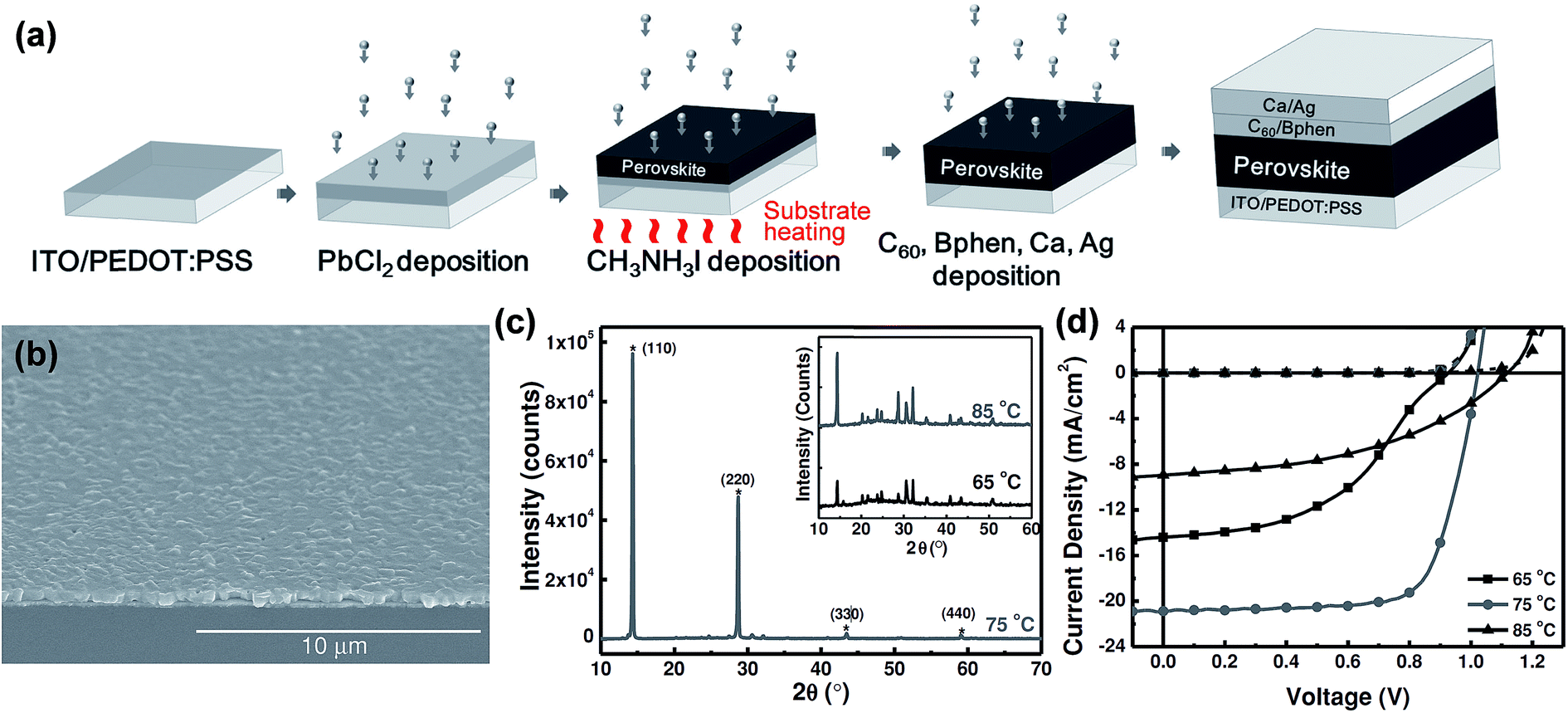 | ||
| Fig. 8 (a) Schematic illustration for the fabrication of perovskite solar cell employing sequential layer-by-layer vacuum deposition. (b) Large area SEM image of the CH3NH3PbI3−xClx thin film fabricated with the substrate temperature held at 75 °C during CH3NH3 sublimation. (c and d) XRD and J–V characteristics of perovskite layers and solar cells with varying substrate temperatures (65 °C, 75 °C, 85 °C) during CH3NH3 sublimation. Reproduced with permission from ref. 88. | ||
Ng et al.90 have employed the deposition of both PbI2 and CH3NH3I at room temperature by decreasing the thickness of both precursor layers. However, an additional subsequent thermal annealing step was necessary for the full conversion to CH3NH3PbI3 perovskite. A multilayered structure consisting of seven alternating depositions of PbI2 (50 nm)/CH3NH3I (50 nm) pairs with subsequent annealing in N2 gas (90 °C, 1 h) generating a CH3NH3PbI3 perovskite film with ∼473 nm thickness and surface roughness of ∼20 nm exhibited the highest average solar cell parameters: Jsc = 20.0 ± 0.8 mA cm−2, Voc = 1.00 ± 0.03 V, FF = 0.57 ± 0.02, and PCE = 11.4 ± 0.5%. Planar structured perovskite solar cells were composed of glass/FTO/c.l.-TiO2/CH3NH3PbI3/spiro-MeOTAD/MoO3/Al layers. The same group of authors investigated the impact of dry-O2 annealing127 of the thermally evaporated CH3NH3PbI3-based solar cells. The results suggested that O2-treatment helped enhance the solar cell performance. Under the optimized conditions, the champion device exhibited: Jsc = 21.8 mA cm−2, Voc = 0.96 V, FF = 0.60, and PCE = 12.5%.90 Low-temperature (max. of 100 °C) fabrication of hole-conductor-free planar perovskite solar cells consisting of only a CH3NH3PbI3/C60 bilayer structure was reported by Hu et al.89 to generate a PCE of 5.4%. Abbas et al.91 have fabricated CH3NH3PbI3 perovskites through sequential deposition of PbI2 in vacuum and subsequently to CH3NH3I after transferring the samples to a graphite vessel. The solar cell devices with FTO/c.l.-TiO2/CH3NH3PbI3/P3HT/Au structure and after optimization of the P3HT layer (thickness ∼ 30 nm and polymer concentration ∼ 12 mg ml−1) have generated high solar cell parameters: Jsc = 21.76 mA cm−2, Voc = 0.96 V, FF = 0.653, and PCE = 13.7%.91 More recently, Yang et al.92 have demonstrated solar cell devices with large active areas of 1 cm2 that exhibit a high PCE of 13.84%, by the alternating layer-by-layer (PbCl2/CH3NH3I) vacuum deposition technique.
Atomic layer deposition (ALD) can be another suitable technique for automatizing the sequential deposition of alternating layers of precursors. ALD is a low-vacuum and low-temperature deposition technique capable of uniform, conformal growth of films over large area with atomic thickness precision. Although, at present, there are no direct processes for the growth of OHPs fully by ALD, alternative protocols have been proposed by Sutherland et al., who showed enhanced optoelectronic properties of ALD processed OHP layers.128,129
6. Flash evaporation or single-source thermal ablation technique
The concept of flash evaporation was first described by Harris and Siegel in 1948 demonstrating the evaporation of metal alloys with controlled stoichiometry.130 Later on, the method was applied for the evaporation of inorganic semiconductor alloys131 as well as oxide-based perovskite materials.132 In 1999, Mitzi et al.97,133 demonstrated that the same technique could be applied for the fabrication of OHP films (named as single source thermal ablation technique). Briefly, the OHP material is initially synthesized by solution processing and spread on a metal heater (e.g. tantalum or molybdenum), Fig. 9a. The dried OHP and heater are loaded into a vacuum chamber. After the system is pumped to vacuum, a large current is passed through the heater causing the OHP material to rapidly evaporate and condense onto a substrate. The desired OHP films are formed when the material is heated rapidly and at high enough temperatures, causing sublimation of the entire compound without thermal decomposition of the organic constituents, Fig. 9a.93,97,133–136 Longo et al.93 have synthesized CH3NH3PbI3 perovskite films by using the flash evaporation technique and showed that smooth surface morphology was obtained with a surface RMS roughness of ∼17.6 nm, Fig. 9b. GIXRD measurements confirmed the formation of stoichiometric CH3NH3PbI3 and revealed high degree of crystallinity, Fig. 9c. Solar cell devices with ITO/PEDOT:PSS/CH3NH3PbI3/polyTPD/PCBM/Ba/Ag layers in a planar heterojunction structure showed respectful solar cell parameters of Jsc = 18 mA cm−2, Voc = 1.067 V, FF = 0.68, and PCE = 12.2%.93 | ||
| Fig. 9 (a) Schematic illustration of the fabrication of perovskite films employing flash evaporation. The precursor solution is spread onto a tantalum foil and mildly annealed obtaining a polycrystalline CH3NH3PbI3 film. The coated tantalum heater is transferred to a vacuum chamber (∼0.1 mbar) where the perovskite is evaporated onto the desired substrate by passing a high current (∼30 A). (b and c) AFM topography and GIXRD pattern of the flash evaporated CH3NH3PbI3 film. (d) J–V characteristics in forward (FWD) and reverse (REV) bias scans for a device with the ITO/PEDOT:PSS/CH3NH3PbI3/polyTPD/PCBM/Ba/Ag structure and under illumination. Reproduced from ref. 93 with permission of The Royal Society of Chemistry. | ||
7. Fundamental understanding of OHP films prepared by vacuum processing
In parallel to several studies focusing on improving the device performance, equal effort has also been made to address the fundamental aspects of the device physics and chemistry. This section is intended to summarize the fundamental understanding earned from the vapor-processed OHPs and solar cells and describe the remaining open questions in this field.The majority of the fundamental aspects of perovskites come from reports on solution-processed perovskites.26,54,112,137–150 Vapor-based systems used for the OHP film synthesis offer unique advantages, i.e., they are compatible with surface science analytical tools and in situ studies. In situ monitoring allows the investigation of events taking place in the OHP films, e.g. during formation or degradation, without altering its pristine conditions that can be influenced by the environmental conditions (e.g. H2O, O2, temperature, light, etc.). In addition, it allows systematic investigation of the influences of controlled environmental conditions (e.g. humidity, O2, temperature, light, etc.) on the material system under study. Pistor et al.151,152 have used a dedicated vacuum chamber system where perovskite film crystalline phase formation from the co-evaporation of PbCl2 and CH3NH3I sources could be monitored in situ and real-time by a built-in XRD setup, Fig. 10a. The PbCl2:CH3NH3I flux ratio was observed as a key parameter for the formation of perovskite films with distinct crystalline phases, Fig. 10b. The CH3NH3I (MAI) source was heated at a constant temperature of 110 °C. The temperature ramp of the PbCl2 source (TPbCl2) was increased steadily from 350 °C to 465 °C. Under low PbCl2 flux conditions, marked with a dotted line (1) in Fig. 10b, the formation of a dark gray/brown CH3NH3PbI3(1−y)Cl3y perovskite film with diffraction peaks at 14.046°, 28.332°, and 31.69°, phase (A), was characteristic. Additional energy dispersive X-ray spectroscopy (EDX) and optical transmission/reflection measurements revealed films with low chlorine content (y = ∼0.02–0.05) and a bandgap of ∼1.6 eV. At higher PbCl2 flux, dotted line (2) in Fig. 10b, XRD revealed formation of a second crystalline phase (B) with peaks at 15.40°, 19.71°, 21.89°, and 35.05°. A chloride-rich phase was identified (y ∼ 1) by EDX with films appearing greenish and transparent. A further increase in temperature of the PbCl2 crucible generates films with pure PbCl2 composition, dotted line (3) in Fig. 10b. In contrast to the Br–I mixed perovskites (CH3NH3PbI3(1−z)Brz) where the formation of solid solution over the whole range (0 < z < 1) was reported,153 the authors of this study concluded that mixed CH3NH3PbI3(1−y)Cly perovskites are not stable for all mixtures between CH3NH3PbI3 and CH3NH3PbCl3. The authors estimated this miscibility gap to be in the range of 0.02 < y < 0.5 and explained it by the increasing difference in the I−–Br−–Cl− ionic radii and was demonstrated by Mosconi et al.154 using first-principle calculations. Ng et al.76 have also studied the formation chemistry of mixed CH3NH3PbI3−xClx perovskites by in situ XPS. PbCl2 was evaporated layer by layer with an increasing total thickness on top of a CH3NH3I film (15 nm) pre-deposited on ITO and XPS Pb 4f, Cl 2p, C 1s, and N 1s core levels were monitored as a function of the PbCl2 thickness. During the initial deposition (0.2 nm to 0.5 nm) the Pb signal was detected, but no Cl signal was observed taking into account the detection limit of the XPS measurement (∼±0.1 atm%). The Cl signal is only observed for a PbCl2 film thickness above 1 nm indicating that PbCl2 can be included when away from the CH3NH3I/PbCl2 interface. The absence of Cl at the CH3NH3I/PbCl2 interface (PbCl2 thickness below 0.5 nm) was attributed as a result of the interaction between PbCl2 and CH3NH3I where Cl− is energetically unfavorable because of the abrupt difference in the ionic radii of Cl− and I− ions.154 These results are also consistent with the low content of chloride identified in solution processed CH3NH3PbI3−xClx perovskite films.26,155,156
 | ||
| Fig. 10 (a) Schematic illustration of the design of a vacuum chamber for perovskite thin film deposition by the multisource evaporation and in situ XRD setup for the real-time monitoring of crystalline phase formation. (b) Time evolution representation of the X-ray diffracted intensity measured during CH3NH3PbI3−xClx formation. The CH3NH3I (MAI) source was operated at a constant temperature of 110 °C. The temperature ramp of the PbCl2 source (TPbCl2) and the film thickness are indicated. Three different crystalline phases named A, B, and C are detected according to the PbCl2:MAI flux ratio and marked with dotted lines (1), (2), and (3), respectively. Reprinted with permission from ref. 151. Copyright (2014) American Chemical Society. | ||
The formation mechanism of pure CH3NH3PbI3 perovskite was studied by Liu et al.157 using in situ XPS on successive depositions of thermally evaporated CH3NH3I on a pre-formed PbI2 film with focus on the double C 1s feature observed, while only one N 1s species was present. The peaks observed at 286.6 eV and 402.7 eV in the BE scale were assigned to the photoelectrons originated from C and N elements in CH3NH3PbI3 perovskite. The low-BE feature at 285.3 eV in C 1s was assigned to CH3I from the dissociation of CH3NH3I to CH3I and NH3. In fact, the assignment of the low-BE feature is still under debate. Ng et al.158 and Li et al.159,160 have also identified more than one peak in the C 1s region and assigned the low BE feature to amorphous carbon (C–C).
Li et al.160 performed in situ XPS and investigated the degradation of co-evaporated CH3NH3PbI3 perovskite films under a controlled environment of dry-O2, and H2O exposures conducted in the vacuum chamber by the aid of high-precision leak-valves. CH3NH3PbI3 was reported to be not sensitive to O2 even at higher exposures of 1013 Langmuir (L, 1 L = 10−6 Torr s). However, a reaction threshold of ∼2 × 10¹⁰ L was found for H2O exposure proposing decomposition of CH3NH3PbI3 to NH3, HI, and PbI2 in agreement with previous reports.161,162
One important requirement for attaining high-efficiency OHP solar cells is to match the electronic energy levels of OHP absorber and the adjacent selective contacts (ETL and HTL) for minimal energy loss and reduced charge recombination.112,142,146 A large collection of energy levels with respect to (w.r.t.) vacuum for the different materials commonly employed in OHP-based solar cells is shown in Fig. 11.17,18,163 The indicated bandgap values for OHPs in Fig. 11 correspond to optical bandgaps (that differs from the transport gap) and all of studies were reported on solution-processed OHPs.164 Few studies exist on the determination of energy levels on vacuum-processed perovskites measured by UPS.157,159,160 The flat band assumption widely considered can still provide a rational judgement when choosing functional layers to be coupled with the OHP layer. However, careful determination of band bending, interfacial states, and interfacial dipoles is important when considering the band alignments of OHP layers with adjacent functional layers.112,142,146,147 In this sense, film deposition by vacuum-methods is suitable for studying the energy alignments because step-wise deposition with controlled incremental amounts of film thickness can be conducted as well as it is directly compatible with UPS and IPES systems. Energy level diagrams at interfaces were determined for the following material systems: CH3NH3PbX/spiro-MeOTAD (X = I3, I3−xClx, Br3),112 CH3NH3PbI3/C60,139 CH3NH3PbI3/Au,139,145 CH3NH3PbI3/MoOx,142,144 CH3NH3PbI3/copper phthalocyanine (CuPc),147 CH3NH3PbIBr2/spiro-MeOTAD,142 CH3NH3PbIBr2/N,N′-di(naphthalene-1-yl)-N,N′-diphenylbenzidine (NPB),142 CH3NH3PbIBr2/copper-hexadecafluorophtalocyanine (F16CuPc),142 and CH3NH3PbIBr2/1,4,5,6,8,11-hexaazatriphenylene hexacarbonitrile (HAT-CN).142
 | ||
| Fig. 11 Summary of literature values for the energy levels with respect to (w.r.t.) the vacuum level (Evac) for the different materials acting as anode and cathode electrodes, electron transport layer, OHP, and hole transport layer. The optical bandgaps are indicated below each type of OHPs. Variations in HOMO, LUMO, and band edge positions are observed in the literature. It is emphasized that the flat band assumption does not hold true when two layers are brought in contact. Reproduced from ref. 18 with permission of The Royal Society of Chemistry. | ||
Hysteresis appears as a manifestation in the J–V curves, where its shape is strongly influenced by the scan direction (forward versus reverse), scan rate, scan history, pre-illumination, and pre-biasing conditions.165–170 It is pointed out that hysteresis in OHP-based solar cells will lead to inaccurate reporting of PCEs, leading to inaccuracies when comparing the different reported PCEs among different laboratories. Stabilized power output under working conditions has been suggested as a useful parameter.165 Efforts have been made on determining the origins of the hysteresis phenomena. Recently, several studies have enforced to ion migration as the main phenomena in determining charge transport in OHP materials.8,170–176 Few studies reported on the hysteresis-free J–V characteristics in vapor-processed OHP solar cells.71,85,88,91,93,177 However, its origin is difficult to be understood from the reported studies as systematic studies are lacking.
8. Conclusions and outlook
The identification of new properties in novel materials is key for generating new technologies. The introduction of well-established inorganic or organic materials led to dramatic improvements in the history of technology. Inorganic silicon-based technology enabled unprecedented development of advanced electronic devices (e.g. laptops, smart phones, digital cameras, Si solar cells, etc.). Organic semiconductors on the other hand have received attention in light-weight, flexible, flat-panel-display and organic light emitting diode applications. The past few years have witnessed a rapid evolution of hybrid organic–inorganic OHP-based solar cells. OHP materials effectively combine the properties of the inorganic framework and the intercalated organic species. As has been reviewed previously, OHP materials show several desirable properties for photovoltaic178–180 and other optoelectronic technologies:181–183 high absorption coefficients, long carrier diffusion lengths, ambipolar carrier transport, shallow defect levels, emission efficiency, and low concentration of defects. Although the operation of vapor based methods often require a certain level of vacuum that is generally perceived as high cost processing, they have been widely employed in the semiconductor industry demonstrating high throughput and reliability. Therefore, a detailed factual cost analysis would be required for evaluating various fabrication methods taking into account the cost-effectiveness in a mass production scenario.184–186When transferring solar cell technology from laboratory scale fabrication know-how to industry-scale production, fabrication cost, efficiency, and lifetime are the three major factors, which are associated together with functionality (e.g. transparency, flexibility, easy integration in tandem cells, etc.).185,187,188 At this stage, despite the superior quality of films prepared by the vapor-deposition method (e.g. uniform and full coverage),4 best efficiencies achieved for OHP solar cells based on vapor-based methods (a PCE of 16.5% with an active area of 0.2 cm2),37 (Table 1) are still somewhat lower than that of the solution-processed cells (a certified PCE of 20.1%). The efficiencies of vapor deposition based perovskite solar cells are still lagging behind their counterpart prepared by solution based methods. On the other hand, we regard this more as a strong motivation to invite more research effort on vapor based methods, rather than an intrinsic disadvantage associated with vapor based methods. Since the ground-breaking work by the groups of Prof. Snaith and Prof. Bolink in 2013 on vapor deposition prepared perovskite solar cells, more and more research groups became interested and have been making contributions to this topic. For example, at this stage it has been demonstrated by a number of groups that vapor based methods provide another viable route to fabricate perovskite solar cells leading to promising efficiencies using both regular and inverted structures (see Table 1 and Fig. 12). Efficiencies as high as 16.5% have been reported so far and the trend of efficiency increase is very clear as shown in Fig. 12. Further improvements on the performance of vapor deposition based perovskite solar cells may come from the following strategies. First of all, multiple reports have indicated that the properties of vapor deposition based perovskite are distinctively different from those prepared by solution processing. Therefore, it is necessary to carry out more in-depth investigations on vapor deposition based perovskite films. Secondly, due to the property difference, the optimal fabrication conditions for vapor deposition based perovskite solar cells are most likely not the same as those for solution prepared ones. A complete set of optimization processes hopefully will provide further efficiency growth of vapor deposition based perovskite solar cells. Thirdly, vapor deposition based perovskite films have some specific advantages, e.g. high degree of uniformity (even at relatively thin film thicknesses) and semitransparency, which may provide the vapor based methods with unique features beyond the pure efficiency considerations. Note that none of the PCE values reported in Table 1 has been certified, which to some degree also underscores the need to further explore these vapor-based methods. In general, caution should be practiced when comparing the cell performance reported by different laboratories as PCE values in OHP solar cells are shown to strongly depend on measurement conditions, such as the voltage-scan polarity (forward versus reverse) and rate, light-soaking, pre-biasing, and cell temperature.168,189 OHP films deposited by vapor-based methods generally show low XRD intensity, but the corresponding solar cells still show relatively high efficiencies. No direct correlation has been reported between XRD peak intensity (generally considered as a measure of crystallinity) and the corresponding solar cell efficiency. In addition, the crystallinity, perovskite composition, and film morphology are strongly dependent on the choice of the substrate (e.g. FTO, TiO2, SiO2/Si, etc.), which is expected to become critical when designing tandem cell architecture: the optimized evaporation conditions may differ according to the substrate on which OHP films are being deposited. With regard to vacuum systems that are usually needed for vapor based processing, special care is required for pumps (especially turbo molecular pumps).
 | ||
| Fig. 12 Progress of solar cell efficiency in vapor-processed perovskite solar cells. The graph was generated based on the reported efficiencies shown in Table 1. A trend of increase in the number of published works on vapor-processed perovskites is inferred from the graph. | ||
For commercialization to take off, large area modules will be required.190,191 A few attempts were made on large area (1 cm2) fabrication based on vacuum- and CVD processes, Table 1, showing a promising PCE as high as 13.84%.92 Because uniform, high-quality, and full-coverage OHP films are achievable, vacuum- and CVD processes are expected to have unique advantages in the fabrication of large-area OHP solar modules.190
The OHP materials are hygroscopic in nature, and are susceptible to degradation upon the intake of moisture.192 Therefore, for protecting the core material in the OHP-based solar cells it requires stringent encapsulation. In addition to extrinsic degradation factors by moisture, the intrinsic stability of perovskites remains a major issue. The chemical reactions between moisture and perovskite need be carefully studied to unravel the reaction pathways, which provide insight for the development of methods (e.g. chemical composition engineering2,153,193) for stabilizing perovskites. The negative standard Gibbs free energy for iodide perovskite degradation was also reported in the absence of moisture.161,192,194 The majority of stability tests reported in the literature, provides the lifetime profiles of OHP solar cells under the storage conditions (in N2 or in ambient air). Only limited data exist for stability profiles under real operating conditions for vacuum- or CVD processed OHP solar cells.109
A major drawback of high efficient OHP solar cells is the use of Pb2+, the material toxicity of which has been emphasized.184,190,195 Efforts have been made to find alternatives such as Sn2+. However, the instability of Sn2+ to form Sn4+ leads to a metal-like behavior and lowers the photovoltaic performance.196 Many other elements in the periodic table (e.g. Co2+, Fe2+, Mn2+, Pd2+, and Ge2+) were suggested as alternatives for Pb2+.24,163 Through comparison with the amount of lead used in lead acid batteries, a much lesser amount of lead is estimated to be required to produce 1000 GW per year from CH3NH3PbI3 perovskite solar cells.197 Therefore, tracking and minimizing the amounts of lead salt as well as quantifying solar cell efficiency normalized by the perovskite amount (e.g. PCE/thickness parameter calculated in Table 1) are proposed as important parameters to evaluate the toxicity at the times of disposal, recycling, and of eventual accidents.184,190,195
Acknowledgements
This work was supported by funding from the Energy Materials and Surface Sciences Unit of the Okinawa Institute of Science and Technology Graduate University and JSPS KAKENHI Grant Number 15K17925.Notes and references
- A. T. Barrows, A. J. Pearson, C. K. Kwak, A. D. F. Dunbar, A. R. Buckley and D. G. Lidzey, Energy Environ. Sci., 2014, 7, 2944–2950 Search PubMed.
- A. Mei, X. Li, L. Liu, Z. Ku, T. Liu, Y. Rong, M. Xu, M. Hu, J. Chen, Y. Yang, M. Grätzel and H. Han, Science, 2014, 345, 295–298 CrossRef CAS PubMed.
- K. Hwang, Y.-S. Jung, Y.-J. Heo, F. H. Scholes, S. E. Watkins, J. Subbiah, D. J. Jones, D.-Y. Kim and D. Vak, Adv. Mater., 2015, 27, 1241–1247 CrossRef CAS PubMed.
- M. Z. Liu, M. B. Johnston and H. J. Snaith, Nature, 2013, 501, 395–398 CrossRef CAS PubMed.
- O. Malinkiewicz, A. Yella, Y. H. Lee, G. M. Espallargas, M. Graetzel, M. K. Nazeeruddin and H. J. Bolink, Nat. Photonics, 2014, 8, 128–132 CrossRef CAS.
- National Renewable Energy Laboratory (NREL), http://www.nrel.gov/ncpv/images/efficiency_chart.jpg.
- W. S. Yang, J. H. Noh, N. J. Jeon, Y. C. Kim, S. Ryu, J. Seo and S. I. Seok, Science, 2015, 348, 1234–1237 CrossRef CAS PubMed.
- Z. Fan, K. Sun and J. Wang, J. Mater. Chem. A, 2015, 3, 18809–18828 CAS.
- Q. Chen, N. de Marco, Y. Yang, T. B. Song, C. C. Chen, H. X. Zhao, Z. R. Hong, H. P. Zhou and Y. Yang, Nano Today, 2015, 10, 355–396 CrossRef CAS.
- T. B. Song, Q. Chen, H. P. Zhou, C. Y. Jiang, H. H. Wang, Y. Yang, Y. S. Liu, J. B. You and Y. Yang, J. Mater. Chem. A, 2015, 3, 9032–9050 CAS.
- S. Kazim, M. K. Nazeeruddin, M. Grätzel and S. Ahmad, Angew. Chem., Int. Ed., 2014, 53, 2812–2824 CrossRef CAS PubMed.
- J. Berry, T. Buonassisi, D. A. Egger, G. Hodes, L. Kronik, Y.-L. Loo, I. Lubomirsky, S. R. Marder, Y. Mastai, J. S. Miller, D. B. Mitzi, Y. Paz, A. M. Rappe, I. Riess, B. Rybtchinski, O. Stafsudd, V. Stevanovic, M. F. Toney, D. Zitoun, A. Kahn, D. Ginley and D. Cahen, Adv. Mater., 2015, 27, 5102–5112 CrossRef CAS PubMed.
- N. G. Park, J. Phys. Chem. Lett., 2013, 4, 2423–2429 CrossRef CAS.
- H. J. Snaith, J. Phys. Chem. Lett., 2013, 4, 3623–3630 CrossRef CAS.
- M. A. Green, A. Ho-Baillie and H. J. Snaith, Nat. Photonics, 2014, 8, 506–514 CrossRef CAS.
- N. G. Park, Mater. Today, 2015, 18, 65–72 CrossRef CAS.
- P. Gao, M. Grätzel and M. K. Nazeeruddin, Energy Environ. Sci., 2014, 7, 2448–2463 CAS.
- S. Q. Luo and W. A. Daoud, J. Mater. Chem. A, 2015, 3, 8992–9010 CAS.
- Y. Rong, L. Liu, A. Mei, X. Li and H. Han, Adv. Energy Mater., 2015, 5, 1501066 Search PubMed.
- H. Kim, K.-G. Lim and T.-W. Lee, Energy Environ. Sci., 2015 10.1039/c5ee02194d.
- G. Giorgi, J.-I. Fujisawa, H. Segawa and K. Yamashita, J. Phys. Chem. Lett., 2013, 4, 4213–4216 CrossRef CAS PubMed.
- G. E. Eperon, G. M. Paterno, R. J. Sutton, A. Zampetti, A. A. Haghighirad, F. Cacialli and H. J. Snaith, J. Mater. Chem. A, 2015, 3, 19688–19695 CAS.
- G. E. Eperon, S. D. Stranks, C. Menelaou, M. B. Johnston, L. M. Herz and H. J. Snaith, Energy Environ. Sci., 2014, 7, 982–988 CAS.
- M. R. Filip, G. E. Eperon, H. J. Snaith and F. Giustino, Nat. Commun., 2014, 5, 5757 CrossRef CAS PubMed.
- M. Grätzel, Nat. Mater., 2014, 13, 838–842 CrossRef PubMed.
- H. Yu, F. Wang, F. Xie, W. Li, J. Chen and N. Zhao, Adv. Funct. Mater., 2014, 24, 7102–7108 CAS.
- C. Wehrenfennig, M. Z. Liu, H. J. Snaith, M. B. Johnston and L. M. Herz, Energy Environ. Sci., 2014, 7, 2269–2275 CAS.
- W.-J. Yin, T. Shi and Y. Yan, Adv. Mater., 2014, 26, 4653–4658 CrossRef CAS PubMed.
- W. J. Yin, J. H. Yang, J. Kang, Y. F. Yan and S. H. Wei, J. Mater. Chem. A, 2015, 3, 8926–8942 CAS.
- J. Kim, S. H. Lee, J. H. Lee and K. H. Hong, J. Phys. Chem. Lett., 2014, 5, 1312–1317 CrossRef CAS PubMed.
- W.-J. Yin, T. Shi and Y. Yan, Appl. Phys. Lett., 2014, 104, 063903 CrossRef.
- D. Li, C. Liang, H. Zhang, C. Zhang, F. You and Z. He, J. Appl. Phys., 2015, 117, 074901 CrossRef.
- C. Wehrenfennig, M. Z. Liu, H. J. Snaith, M. B. Johnston and L. M. Herz, J. Phys. Chem. Lett., 2014, 5, 1300–1306 CrossRef CAS PubMed.
- D. W. deQuilettes, S. M. Vorpahl, S. D. Stranks, H. Nagaoka, G. E. Eperon, M. E. Ziffer, H. J. Snaith and D. S. Ginger, Science, 2015, 348, 683–686 CrossRef CAS PubMed.
- V. D'Innocenzo, G. Grancini, M. J. Alcocer, A. R. Kandada, S. D. Stranks, M. M. Lee, G. Lanzani, H. J. Snaith and A. Petrozza, Nat. Commun., 2014, 5, 3586 Search PubMed.
- A. Marchioro, J. Teuscher, D. Friedrich, M. Kunst, R. van de Krol, T. Moehl, M. Grätzel and J. E. Moser, Nat. Photonics, 2014, 8, 250–255 CrossRef CAS.
- Q. Lin, A. Armin, R. C. R. Nagiri, P. L. Burn and P. Meredith, Nat. Photonics, 2015, 9, 106–112 CrossRef CAS.
- M. Hirasawa, T. Ishihara, T. Goto, K. Uchida and N. Miura, Phys. B, 1994, 201, 427–430 CrossRef CAS.
- J. M. Frost, K. T. Butler, F. Brivio, C. H. Hendon, M. van Schilfgaarde and A. Walsh, Nano Lett., 2014, 14, 2584–2590 CrossRef CAS PubMed.
- C. R. Kagan, D. B. Mitzi and C. D. Dimitrakopoulos, Science, 1999, 286, 945–947 CrossRef CAS PubMed.
- D. B. Mitzi, Chem. Mater., 2001, 13, 3283–3298 CrossRef CAS.
- D. B. Mitzi, K. Chondroudis and C. R. Kagan, IBM J. Res. Dev., 2001, 45, 29–45 CrossRef CAS.
- B. O'Regan and M. Grätzel, Nature, 1991, 353, 737–740 CrossRef.
- U. Bach, D. Lupo, P. Comte, J. E. Moser, F. Weissortel, J. Salbeck, H. Spreitzer and M. Grätzel, Nature, 1998, 395, 583–585 CrossRef CAS.
- A. Kojima, K. Teshima, Y. Shirai and T. Miyasaka, J. Am. Chem. Soc., 2009, 131, 6050–6051 CrossRef CAS PubMed.
- H. S. Kim, C. R. Lee, J. H. Im, K. B. Lee, T. Moehl, A. Marchioro, S. J. Moon, R. Humphry-Baker, J. H. Yum, J. E. Moser, M. Grätzel and N. G. Park, Sci. Rep., 2012, 2, 591 Search PubMed.
- M. M. Lee, J. Teuscher, T. Miyasaka, T. N. Murakami and H. J. Snaith, Science, 2012, 338, 643–647 CrossRef CAS PubMed.
- H. S. Kim, S. H. Im and N. G. Park, J. Phys. Chem. C, 2014, 118, 5615–5625 CAS.
- S. Kazim, M. K. Nazeeruddin, M. Grätzel and S. Ahmad, Angew. Chem., Int. Ed., 2014, 53, 2812–2824 CrossRef CAS PubMed.
- H. Zhou, Q. Chen, G. Li, S. Luo, T.-b. Song, H.-S. Duan, Z. Hong, J. You, Y. Liu and Y. Yang, Science, 2014, 345, 542–546 CrossRef CAS PubMed.
- L. Etgar, P. Gao, Z. Xue, Q. Peng, A. K. Chandiran, B. Liu, M. K. Nazeeruddin and M. Grätzel, J. Am. Chem. Soc., 2012, 134, 17396–17399 CrossRef CAS PubMed.
- E. J. Juarez-Perez, M. Wuβler, F. Fabregat-Santiago, K. Lakus-Wollny, E. Mankel, T. Mayer, W. Jaegermann and I. Mora-Sero, J. Phys. Chem. Lett., 2014, 5, 680–685 CrossRef CAS PubMed.
- K. Wojciechowski, M. Saliba, T. Leijtens, A. Abate and H. J. Snaith, Energy Environ. Sci., 2014, 7, 1142–1147 CAS.
- B. Conings, L. Baeten, C. De Dobbelaere, J. D'Haen, J. Manca and H. G. Boyen, Adv. Mater., 2014, 26, 2041–2046 CrossRef CAS PubMed.
- B. Cai, Y. Xing, Z. Yang, W.-H. Zhang and J. Qiu, Energy Environ. Sci., 2013, 6, 1480–1485 CAS.
- E. Edri, S. Kirmayer, D. Cahen and G. Hodes, J. Phys. Chem. Lett., 2013, 4, 897–902 CrossRef CAS PubMed.
- J. T. W. Wang, J. M. Ball, E. M. Barea, A. Abate, J. A. Alexander-Webber, J. Huang, M. Saliba, I. Mora-Sero, J. Bisquert, H. J. Snaith and R. J. Nicholas, Nano Lett., 2014, 14, 724–730 CrossRef CAS PubMed.
- K. N. Liang, D. B. Mitzi and M. T. Prikas, Chem. Mater., 1998, 10, 403–411 CrossRef CAS.
- J. Burschka, N. Pellet, S. J. Moon, R. Humphry-Baker, P. Gao, M. K. Nazeeruddin and M. Grätzel, Nature, 2013, 499, 316–319 CrossRef CAS.
- D. Q. Bi, S. J. Moon, L. Haggman, G. Boschloo, L. Yang, E. M. J. Johansson, M. K. Nazeeruddin, M. Grätzel and A. Hagfeldt, RSC Adv., 2013, 3, 18762–18766 RSC.
- Y. Y. Zhou, M. J. Yang, W. W. Wu, A. L. Vasiliev, K. Zhu and N. P. Padture, J. Mater. Chem. A, 2015, 3, 8178–8184 CAS.
- Q. Chen, H. Zhou, Z. Hong, S. Luo, H.-S. Duan, H.-H. Wang, Y. Liu, G. Li and Y. Yang, J. Am. Chem. Soc., 2013, 136, 622–625 CrossRef PubMed.
- Q. Chen, H. Zhou, T.-B. Song, S. Luo, Z. Hong, H.-S. Duan, L. Dou, Y. Liu and Y. Yang, Nano Lett., 2014, 14, 4158–4163 CrossRef CAS PubMed.
- C. Ying, C. W. Shi, N. Wu, J. C. Zhang and M. Wang, Nanoscale, 2015, 7, 12092–12095 RSC.
- H. Zhou, Q. Chen and Y. Yang, MRS Bull., 2015, 40, 667–673 CrossRef CAS.
- G. Balaji, P. H. Joshi, H. A. Abbas, L. Zhang, R. Kottokkaran, M. Samiee, M. Noack and V. L. Dalal, Phys. Chem. Chem. Phys., 2015, 17, 10369–10372 RSC.
- R. Sheng, A. Ho-Baillie, S. J. Huang, S. Chen, X. M. Wen, X. J. Hao and M. A. Green, J. Phys. Chem. C, 2015, 119, 3545–3549 CAS.
- Y. B. Li, J. K. Cooper, R. Buonsanti, C. Giannini, Y. Liu, F. M. Toma and I. D. Sharp, J. Phys. Chem. Lett., 2015, 6, 493–499 CrossRef CAS PubMed.
- T. Du, N. Wang, H. Chen, H. Lin and H. He, ACS Appl. Mater. Interfaces, 2015, 7, 3382–3388 CAS.
- C. Momblona, O. Malinkiewicz, C. Roldán-Carmona, A. Soriano, L. Gil-Escrig, E. Bandiello, M. Scheepers, E. Edri and H. J. Bolink, APL Mater., 2014, 2, 081504 CrossRef.
- O. Malinkiewicz, C. Roldán-Carmona, A. Soriano, E. Bandiello, L. Camacho, M. K. Nazeeruddin and H. J. Bolink, Adv. Energy Mater., 2014, 4, 1400345 Search PubMed.
- A. S. Subbiah, A. Halder, S. Ghosh, N. Mahuli, G. Hodes and S. K. Sarkar, J. Phys. Chem. Lett., 2014, 5, 1748–1753 CrossRef CAS PubMed.
- B. S. Kim, T. M. Kim, M. S. Choi, H. S. Shim and J. J. Kim, Org. Electron., 2015, 17, 102–106 CrossRef CAS.
- L. E. Polander, P. Pahner, M. Schwarze, M. Saalfrank, C. Koerner and K. Leo, APL Mater., 2014, 2, 081503 CrossRef.
- M. Sessolo, C. Momblona, L. Gil-Escrig and H. J. Bolink, MRS Bull., 2015, 40, 660–666 CrossRef CAS.
- T.-W. Ng, C.-Y. Chan, M.-F. Lo, Z. Q. Guan and C.-S. Lee, J. Mater. Chem. A, 2015, 3, 9081–9085 CAS.
- C. Gao, J. Liu, C. Liao, Q. Y. Ye, Y. Z. Zhang, X. L. He, X. W. Guo, J. Mei and W. M. Lau, RSC Adv., 2015, 5, 26175–26180 RSC.
- L. K. Ono, S. Wang, Y. Kato, S. R. Raga and Y. B. Qi, Energy Environ. Sci., 2014, 7, 3989–3993 CAS.
- S. Wang, L. K. Ono, M. R. Leyden, Y. Kato, S. R. Raga, M. V. Lee and Y. B. Qi, J. Mater. Chem. A, 2015, 3, 14631–14641 CAS.
- J. Teuscher, A. Ulianov, O. Müntener, M. Grätzel and N. Tétreault, ChemSusChem, 2015, 8, 3847–3852 CrossRef CAS PubMed.
- D. Zhao, W. Ke, C. R. Grice, A. J. Cimaroli, X. Tan, M. Yang, R. W. Collins, H. Zhang, K. Zhu and Y. Yan, Nano Energy, 2015, 19, 88–97 CrossRef.
- M. R. Leyden, L. K. Ono, S. R. Raga, Y. Kato, S. H. Wang and Y. B. Qi, J. Mater. Chem. A, 2014, 2, 18742–18745 CAS.
- M. R. Leyden, M. V. Lee, S. R. Raga and Y. B. Qi, J. Mater. Chem. A, 2015, 3, 16097–16103 CAS.
- P. F. Luo, Z. F. Liu, W. Xia, C. C. Yuan, J. G. Cheng and Y. W. Lu, J. Mater. Chem. A, 2015, 3, 12443–12451 CAS.
- P. F. Luo, Z. F. Liu, W. Xia, C. C. Yuan, J. G. Cheng and Y. W. Lu, ACS Appl. Mater. Interfaces, 2015, 7, 2708–2714 CAS.
- P. Luo, Z. Liu, W. Xia, C. Yuan, J. Cheng, C. Xu and Y. Lu, J. Mater. Chem. A, 2015, 3, 22949–22959 CAS.
- Y. Peng, G. Jing and T. Cui, RSC Adv., 2015, 5, 95847–95853 RSC.
- C.-W. Chen, H.-W. Kang, S.-Y. Hsiao, P.-F. Yang, K.-M. Chiang and H.-W. Lin, Adv. Mater., 2014, 26, 6647–6652 CrossRef CAS PubMed.
- H. Hu, D. Wang, Y. Y. Zhou, J. L. Zhang, S. L. Lv, S. P. Pang, X. Chen, Z. H. Liu, N. P. Padture and G. L. Cui, RSC Adv., 2014, 4, 28964–28967 RSC.
- A. Ng, Z. Ren, Q. Shen, S. H. Cheung, H. C. Gokkaya, G. Bai, J. Wang, L. Yang, S. K. So, A. B. Djurisic, W. W.-f. Leung, J. Hao, W. K. Chan and C. Surya, J. Mater. Chem. A, 2015, 3, 9223–9231 CAS.
- H. A. Abbas, R. Kottokkaran, B. Ganapathy, M. Samiee, L. Zhang, A. Kitahara, M. Noack and V. L. Dalal, APL Mater., 2015, 3, 016105 CrossRef.
- D. Yang, Z. Yang, W. Qin, Y. L. Zhang, S. Z. Liu and C. Li, J. Mater. Chem. A, 2015, 3, 9401–9405 CAS.
- G. Longo, L. Gil-Escrig, M. J. Degen, M. Sessolo and H. J. Bolink, Chem. Commun., 2015, 51, 7376–7378 RSC.
- A. Dualeh, N. Tétreault, T. Moehl, P. Gao, M. K. Nazeeruddin and M. Grätzel, Adv. Funct. Mater., 2014, 24, 3250–3258 CrossRef CAS.
- G. E. Eperon, V. M. Burlakov, P. Docampo, A. Goriely and H. J. Snaith, Adv. Funct. Mater., 2014, 24, 151–157 CrossRef CAS.
- P.-W. Liang, C.-Y. Liao, C.-C. Chueh, F. Zuo, S. T. Williams, X.-K. Xin, J. Lin and A. K. Y. Jen, Adv. Mater., 2014, 26, 3748–3754 CrossRef CAS PubMed.
- D. B. Mitzi, M. T. Prikas and K. Chondroudis, Chem. Mater., 1999, 11, 542–544 CrossRef CAS.
- N. J. Jeon, J. H. Noh, W. S. Yang, Y. C. Kim, S. Ryu, J. Seo and S. I. Seok, Nature, 2015, 517, 476–480 CrossRef CAS PubMed.
- D. T. Moore, H. Sai, K. W. Tan, D.-M. Smilgies, W. Zhang, H. J. Snaith, U. Wiesner and L. A. Estroff, J. Am. Chem. Soc., 2015, 137, 2350–2358 CrossRef CAS.
- M. Toshinori, F. Katsuhiko and T. Tetsuo, Jpn. J. Appl. Phys., 2006, 45, 523 CrossRef.
- F. Hao, C. C. Stoumpos, Z. Liu, R. P. H. Chang and M. G. Kanatzidis, J. Am. Chem. Soc., 2014, 136, 16411–16419 CrossRef CAS PubMed.
- J. B. You, Y. M. Yang, Z. R. Hong, T. B. Song, L. Meng, Y. S. Liu, C. Y. Jiang, H. P. Zhou, W. H. Chang, G. Li and Y. Yang, Appl. Phys. Lett., 2014, 105, 183902 CrossRef.
- N. J. Jeon, J. H. Noh, Y. C. Kim, W. S. Yang, S. Ryu and S. I. Seok, Nat. Mater., 2014, 13, 897–903 CrossRef CAS PubMed.
- M. Era, T. Hattori, T. Taira and T. Tsutsui, Chem. Mater., 1997, 9, 8–10 CrossRef CAS.
- A. M. Salau, Sol. Energy Mater., 1980, 2, 327–332 CrossRef CAS.
- L. K. Ono, P. Schulz, J. J. Endres, G. O. Nikiforov, Y. Kato, A. Kahn and Y. B. Qi, J. Phys. Chem. Lett., 2014, 5, 1374–1379 CrossRef CAS PubMed.
- Z. Hawash, L. K. Ono, S. R. Raga, M. V. Lee and Y. B. Qi, Chem. Mater., 2015, 27, 562–569 CrossRef CAS.
- M. C. Jung, S. R. Raga, L. K. Ono and Y. B. Qi, Sci. Rep., 2015, 5, 9863 CrossRef CAS PubMed.
- L. K. Ono, S. R. Raga, M. Remeika, A. J. Winchester, A. Gabe and Y. B. Qi, J. Mater. Chem. A, 2015, 3, 15451–15456 CAS.
- J. A. Christians, R. C. M. Fung and P. V. Kamat, J. Am. Chem. Soc., 2014, 136, 758–764 CrossRef CAS PubMed.
- S. Ito, S. Tanaka, H. Vahlman, H. Nishino, K. Manabe and P. Lund, ChemPhysChem, 2014, 15, 1194–1200 CrossRef CAS PubMed.
- P. Schulz, E. Edri, S. Kirmayer, G. Hodes, D. Cahen and A. Kahn, Energy Environ. Sci., 2014, 7, 1377–1381 CAS.
- R. F. Service, Science, 2014, 344, 458 CrossRef PubMed.
- G. E. Eperon, V. M. Burlakov, A. Goriely and H. J. Snaith, ACS Nano, 2014, 8, 591–598 CrossRef CAS PubMed.
- Y. Zhao and K. Zhu, J. Phys. Chem. C, 2014, 118, 9412–9418 CAS.
- R. S. Sanchez, V. Gonzalez-Pedro, J.-W. Lee, N.-G. Park, Y. S. Kang, I. Mora-Sero and J. Bisquert, J. Phys. Chem. Lett., 2014, 5, 2357–2363 CrossRef CAS PubMed.
- V. Gonzalez-Pedro, E. J. Juarez-Perez, W.-S. Arsyad, E. M. Barea, F. Fabregat-Santiago, I. Mora-Sero and J. Bisquert, Nano Lett., 2014, 14, 888–893 CrossRef CAS PubMed.
- B. Wang and T. Chen, Adv. Sci., 2015 DOI:10.1002/advs.201500262.
- Y. K. Peng, G. S. Jing and T. H. Cui, J. Mater. Chem. A, 2015, 3, 12436–12442 CAS.
- S. T. Ha, X. Liu, Q. Zhang, D. Giovanni, T. C. Sum and Q. Xiong, Adv. Opt. Mater., 2014, 2, 838–844 CrossRef CAS.
- Q. Zhang, S. T. Ha, X. Liu, T. C. Sum and Q. Xiong, Nano Lett., 2014, 14, 5995–6001 CrossRef CAS.
- J. Xing, X. F. Liu, Q. Zhang, S. T. Ha, Y. W. Yuan, C. Shen, T. C. Sum and Q. Xiong, Nano Lett., 2015, 15, 4571–4577 CrossRef CAS PubMed.
- D. J. Lewis and P. O'Brien, Chem. Commun., 2014, 50, 6319–6321 RSC.
- D. S. Bhachu, D. O. Scanlon, E. J. Saban, H. Bronstein, I. P. Parkin, C. J. Carmalt and R. G. Palgrave, J. Mater. Chem. A, 2015, 3, 9071–9073 CAS.
- M. M. Tavakoli, L. Gu, Y. Gao, C. Reckmeier, J. He, A. L. Rogach, Y. Yao and Z. Fan, Sci. Rep., 2015, 5, 14083 CrossRef PubMed.
- M. Era, K. Maeda and T. Tsutsui, Thin Solid Films, 1998, 331, 285–290 CrossRef CAS.
- Z. Ren, A. Ng, Q. Shen, H. C. Gokkaya, J. Wang, L. Yang, W.-K. Yiu, G. Bai, A. B. Djurišić, W. W.-f. Leung, J. Hao, W. K. Chan and C. Surya, Sci. Rep., 2014, 4, 6752 CrossRef PubMed.
- B. R. Sutherland, S. Hoogland, M. M. Adachi, P. Kanjanaboos, C. T. O. Wong, J. J. McDowell, J. X. Xu, O. Voznyy, Z. J. Ning, A. J. Houtepen and E. H. Sargent, Adv. Mater., 2015, 27, 53–58 CrossRef CAS PubMed.
- B. R. Sutherland, S. Hoogland, M. M. Adachi, C. T. O. Wong and E. H. Sargent, ACS Nano, 2014, 8, 10947–10952 CrossRef CAS PubMed.
- L. Harris and B. M. Siegel, J. Appl. Phys., 1948, 19, 739–741 CrossRef CAS.
- J. L. Richards, P. B. Hart and L. M. Gallone, J. Appl. Phys., 1963, 34, 3418–3420 CrossRef CAS.
- E. K. Müller, B. J. Nicholson and G. L. E. Turner, J. Electrochem. Soc., 1963, 110, 969–973 CrossRef.
- K. Chondroudis, D. B. Mitzi and P. Brock, Chem. Mater., 2000, 12, 169–175 CrossRef CAS.
- F. Chiarella, A. Zappettini, F. Licci, I. Borriello, G. Cantele, D. Ninno, A. Cassinese and R. Vaglio, Phys. Rev. B: Condens. Matter Mater. Phys., 2008, 77, 045129 CrossRef.
- S. Ahmad, C. Hanmandlu, P. K. Kanaujia and G. V. Prakash, Opt. Mater. Express, 2014, 4, 1313–1323 CrossRef CAS.
- G.-X. Liang, P. Fan, J.-T. Luo, D. Gu and Z.-H. Zheng, Prog. Photovolt: Res. Appl., 2015, 23, 1901–1907 CrossRef CAS.
- S. R. Raga, M.-C. Jung, M. V. Lee, M. R. Leyden, Y. Kato and Y. B. Qi, Chem. Mater., 2015, 27, 1597–1603 CrossRef CAS.
- T. Miyadera, Y. Shibata, T. Koganezawa, T. N. Murakami, T. Sugita, N. Tanigaki and M. Chikamatsu, Nano Lett., 2015, 15, 5630–5634 CrossRef CAS PubMed.
- C. G. Wang, X. L. Liu, C. C. Wang, Z. G. Xiao, C. Bi, Y. C. Shao, J. S. Huang and Y. L. Gao, J. Vac. Sci. Technol., B, 2015, 33, 032401 Search PubMed.
- A. Calloni, A. Abate, G. Bussetti, G. Berti, R. Yivlialin, F. Ciccacci and L. Duò, J. Phys. Chem. C, 2015, 119, 21329–21335 CAS.
- R. Lindblad, D. Bi, B.-w. Park, J. Oscarsson, M. Gorgoi, H. Siegbahn, M. Odelius, E. M. J. Johansson and H. Rensmo, J. Phys. Chem. Lett., 2014, 5, 648–653 CrossRef CAS PubMed.
- Q. K. Wang, R. B. Wang, P. F. Shen, C. Li, Y. Q. Li, L. J. Liu, S. Duhm and J. X. Tang, Adv. Mater. Interfaces, 2015, 2, 1400528 Search PubMed.
- L. A. Frolova, N. N. Dremova and P. A. Troshin, Chem. Commun., 2015, 51, 14917–14920 RSC.
- P. Liu, X. L. Liu, L. Lyu, H. P. Xie, H. Zhang, D. M. Niu, H. Huang, C. Bi, Z. G. Xiao, J. S. Huang and Y. L. Gao, Appl. Phys. Lett., 2015, 106, 193903 CrossRef.
- X. L. Liu, C. G. Wang, L. Lyu, C. C. Wang, Z. G. Xiao, C. Bi, J. S. Huang and Y. L. Gao, Phys. Chem. Chem. Phys., 2015, 17, 896–902 RSC.
- E. M. Miller, Y. X. Zhao, C. C. Mercado, S. K. Saha, J. M. Luther, K. Zhu, V. Stevanovic, C. L. Perkins and J. van de Lagemaat, Phys. Chem. Chem. Phys., 2014, 16, 22122–22130 RSC.
- S. Chen, T. W. Goh, D. Sabba, J. Chua, N. Mathews, C. H. A. Huan and T. C. Sum, APL Mater., 2014, 2, 081512 CrossRef.
- Q. Wang, Y. Shao, H. Xie, L. Lyu, X. Liu, Y. Gao and J. Huang, Appl. Phys. Lett., 2014, 105, 163508 CrossRef.
- B. J. Foley, D. L. Marlowe, K. Y. Sun, W. A. Saidi, L. Scudiero, M. C. Gupta and J. J. Choi, Appl. Phys. Lett., 2015, 106, 243904 CrossRef.
- I. Deretzis, A. Alberti, G. Pellegrino, E. Smecca, F. Giannazzo, N. Sakai, T. Miyasaka and A. La Magna, Appl. Phys. Lett., 2015, 106, 131904 CrossRef.
- P. Pistor, J. Borchert, W. Fränzel, R. Csuk and R. Scheer, J. Phys. Chem. Lett., 2014, 5, 3308–3312 CrossRef CAS PubMed.
- J. Borchert, H. Boht, W. Franzel, R. Csuk, R. Scheer and P. Pistor, J. Mater. Chem. A, 2015, 3, 19842–19849 CAS.
- J. H. Noh, S. H. Im, J. H. Heo, T. N. Mandal and S. I. Seok, Nano Lett., 2013, 13, 1764–1769 CrossRef CAS PubMed.
- E. Mosconi, A. Amat, M. K. Nazeeruddin, M. Grätzel and F. de Angelis, J. Phys. Chem. C, 2013, 117, 13902–13913 CAS.
- S. Colella, E. Mosconi, P. Fedeli, A. Listorti, F. Gazza, F. Orlandi, P. Ferro, T. Besagni, A. Rizzo, G. Calestani, G. Gigli, F. de Angelis and R. Mosca, Chem. Mater., 2013, 25, 4613–4618 CrossRef CAS.
- M. I. Dar, N. Arora, P. Gao, S. Ahmad, M. Grätzel and M. K. Nazeeruddin, Nano Lett., 2014, 14, 6991–6996 CrossRef CAS PubMed.
- L. Liu, J. A. McLeod, R. Wang, P. Shen and S. Duhm, Appl. Phys. Lett., 2015, 107, 061904 CrossRef.
- T. W. Ng, C. Y. Chan, Q. D. Yang, H. X. Wei, M. F. Lo, V. A. L. Roy, W. J. Zhang and C. S. Lee, Org. Electron., 2013, 14, 2743–2747 CrossRef CAS.
- Y. Li, X. Xu, C. Wang, C. Wang, F. Xie, J. Yang and Y. Gao, AIP Adv., 2015, 5, 097111 CrossRef.
- Y. Li, X. Xu, C. Wang, C. Wang, F. Xie, J. Yang and Y. Gao, J. Phys. Chem. C, 2015, 119, 23996–24002 CAS.
- G. D. Niu, X. D. Guo and L. D. Wang, J. Mater. Chem. A, 2015, 3, 8970–8980 CAS.
- T. Leijtens, G. E. Eperon, N. K. Noel, S. N. Habisreutinger, A. Petrozza and H. J. Snaith, Adv. Energy Mater., 2015, 5, 1500963 Search PubMed.
- P. P. Boix, K. Nonomura, N. Mathews and S. G. Mhaisalkar, Mater. Today, 2014, 17, 16–23 CrossRef CAS.
- D. Cahen, A. Kahn and E. Umbach, Mater. Today, 2005, 8, 32–41 CrossRef CAS.
- H. J. Snaith, A. Abate, J. M. Ball, G. E. Eperon, T. Leijtens, N. K. Noel, S. D. Stranks, J. T.-W. Wang, K. Wojciechowski and W. Zhang, J. Phys. Chem. Lett., 2014, 5, 1511–1515 CrossRef CAS PubMed.
- H.-S. Kim and N.-G. Park, J. Phys. Chem. Lett., 2014, 5, 2927–2934 CrossRef CAS PubMed.
- E. L. Unger, E. T. Hoke, C. D. Bailie, W. H. Nguyen, A. R. Bowring, T. Heumuller, M. G. Christoforo and M. D. McGehee, Energy Environ. Sci., 2014, 7, 3690–3698 CAS.
- L. K. Ono, S. R. Raga, S. Wang, Y. Kato and Y. B. Qi, J. Mater. Chem. A, 2015, 3, 9074–9080 CAS.
- W. Tress, N. Marinova, T. Moehl, S. M. Zakeeruddin, M. K. Nazeeruddin and M. Grätzel, Energy Environ. Sci., 2015, 8, 995–1004 CAS.
- B. Wu, K. Fu, N. Yantara, G. Xing, S. Sun, T. C. Sum and N. Mathews, Adv. Energy Mater., 2015, 5, 1500829 Search PubMed.
- Z. Xiao, Y. Yuan, Y. Shao, Q. Wang, Q. Dong, C. Bi, P. Sharma, A. Gruverman and J. Huang, Nat. Mater., 2015, 14, 193–198 CrossRef CAS PubMed.
- Y. Zhao, C. J. Liang, H. M. Zhang, D. Li, D. Tian, G. B. Li, X. P. Jing, W. G. Zhang, W. K. Xiao, Q. Liu, F. J. Zhang and Z. Q. He, Energy Environ. Sci., 2015, 8, 1256–1260 CAS.
- Y. Zhang, M. Liu, G. E. Eperon, T. C. Leijtens, D. McMeekin, M. Saliba, W. Zhang, M. de Bastiani, A. Petrozza, L. M. Herz, M. B. Johnston, H. Lin and H. J. Snaith, Mater. Horiz., 2015, 2, 315–322 RSC.
- J. M. Azpiroz, E. Mosconi, J. Bisquert and F. de Angelis, Energy Environ. Sci., 2015, 8, 2118–2127 CAS.
- C. Zhao, B. Chen, X. Qiao, L. Luan, K. Lu and B. Hu, Adv. Energy Mater., 2015, 5, 1500279 Search PubMed.
- J. Beilsten-Edmands, G. E. Eperon, R. D. Johnson, H. J. Snaith and P. G. Radaelli, Appl. Phys. Lett., 2015, 106, 173502 CrossRef.
- A. Dualeh, T. Moehl, N. Tétreault, J. Teuscher, P. Gao, M. K. Nazeeruddin and M. Grätzel, ACS Nano, 2014, 8, 362–373 CrossRef CAS PubMed.
- M. Kaltenbrunner, G. Adam, E. D. Glowacki, M. Drack, R. Schwodiauer, L. Leonat, D. H. Apaydin, H. Groiss, M. C. Scharber, M. S. White, N. S. Sariciftci and S. Bauer, Nat. Mater., 2015, 14, 1032 CrossRef CAS PubMed.
- J. S. Luo, J. H. Im, M. T. Mayer, M. Schreier, M. K. Nazeeruddin, N. G. Park, S. D. Tilley, H. J. Fan and M. Grätzel, Science, 2014, 345, 1593–1596 CrossRef CAS PubMed.
- J. T. Xu, Y. H. Chen and L. M. Dai, Nat. Commun., 2015, 6, 8103 CrossRef CAS PubMed.
- Z. K. Tan, R. S. Moghaddam, M. L. Lai, P. Docampo, R. Higler, F. Deschler, M. Price, A. Sadhanala, L. M. Pazos, D. Credgington, F. Hanusch, T. Bein, H. J. Snaith and R. H. Friend, Nat. Nanotechnol., 2014, 9, 687–692 CrossRef CAS PubMed.
- H. Zhu, Y. Fu, F. Meng, X. Wu, Z. Gong, Q. Ding, M. V. Gustafsson, M. T. Trinh, S. Jin and X. Y. Zhu, Nat. Mater., 2015, 14, 636–642 CrossRef CAS PubMed.
- L. Dou, Y. Yang, J. You, Z. Hong, W.-H. Chang, G. Li and Y. Yang, Nat. Commun., 2014, 5, 5404 CrossRef CAS PubMed.
- N. Espinosa, L. Serrano-Lujan, A. Urbina and F. C. Krebs, Sol. Energy Mater. Sol. Cells, 2015, 137, 303–310 CrossRef CAS.
- B. E. Hardin, H. J. Snaith and M. D. McGehee, Nat. Photonics, 2012, 6, 162–169 CrossRef CAS.
- A. A. Asif, R. Singh and G. F. Alapatt, J. Renewable Sustainable Energy, 2015, 7, 043120 CrossRef.
- A. Fakharuddin, R. Jose, T. M. Brown, F. Fabregat-Santiago and J. Bisquert, Energy Environ. Sci., 2014, 7, 3952–3981 CAS.
- W. Chen, Y. Wu, Y. Yue, J. Liu, W. Zhang, X. Yang, H. Chen, E. Bi, I. Ashraful, M. Grätzel and L. Han, Science, 2015, 350, 944–948 CrossRef CAS PubMed.
- J. A. Christians, J. S. Manser and P. V. Kamat, J. Phys. Chem. Lett., 2015, 6, 852–857 CrossRef CAS PubMed.
- J. Gong, S. B. Darling and F. Q. You, Energy Environ. Sci., 2015, 8, 1953–1968 CAS.
- S. Razza, F. Di Giacomo, F. Matteocci, L. Cinà, A. L. Palma, S. Casaluci, P. Cameron, A. D'Epifanio, S. Licoccia, A. Reale, T. M. Brown and A. Di Carlo, J. Power Sources, 2015, 277, 286–291 CrossRef CAS.
- Y. Kato, L. K. Ono, M. V. Lee, S. H. Wang, S. R. Raga and Y. B. Qi, Adv. Mater. Interfaces, 2015, 2, 1500195 Search PubMed.
- N. Pellet, P. Gao, G. Gregori, T.-Y. Yang, M. K. Nazeeruddin, J. Maier and M. Grätzel, Angew. Chem., Int. Ed., 2014, 53, 3151–3157 CrossRef CAS PubMed.
- A. Alberti, I. Deretzis, G. Pellegrino, C. Bongiorno, E. Smecca, G. Mannino, F. Giannazzo, G. G. Condorelli, N. Sakai, T. Miyasaka, C. Spinella and A. La Magna, ChemPhysChem, 2015, 16, 3064–3071 CrossRef CAS PubMed.
- L. Serrano-Lujan, N. Espinosa, T. T. Larsen-Olsen, J. Abad, A. Urbina and F. C. Krebs, Adv. Energy Mater., 2015, 5, 1501119 Search PubMed.
- C. C. Stoumpos, C. D. Malliakas and M. G. Kanatzidis, Inorg. Chem., 2013, 52, 9019–9038 CrossRef CAS PubMed.
- G. Hodes, Science, 2013, 342, 317–318 CrossRef CAS PubMed.
Footnote |
| † These authors contributed equally. |
| This journal is © The Royal Society of Chemistry 2016 |