DOI:
10.1039/C5SC03807C
(Edge Article)
Chem. Sci., 2016,
7, 896-904
Aromatic hydrocarbon macrocycles for highly efficient organic light-emitting devices with single-layer architectures†
Received
7th October 2015
, Accepted 31st October 2015
First published on 4th November 2015
Abstract
A modern electrophosphorescent organic light-emitting device (OLED) achieves quantitative electro-optical conversion by using multiple layers of molecular materials designed through role allotment for independent and specific functions. A unique, potentially innovative device architecture, i.e., a single-layer phosphorescent OLED, is currently being developed by designing multirole base materials via a structural combination of multiple functional components in single molecules. The multirole molecules, however, inevitably require multiple processes to synthesize their multiple components and, moreover, to assemble these components synthetically into one molecule. We herein show that the multirole base material for a highly efficient single-layer phosphorescent OLED can be designed and synthesized with a single, very simple aromatic hydrocarbon component of toluene merely through a one-pot macrocyclization. Without requiring the assembly tasks at the synthesis stage, the molecular design allows for a concise one-pot synthesis of, and a quantitative electro-optical conversion in, the single-layer device architecture with a single-component base material.
Introduction
An aromatic hydrocarbon, anthracene, was the first material to achieve direct-current electroluminescence.1,2 Although the discovery of the electroluminescence in this hydrocarbon marked the first, preliminary step toward an organic light-emitting device (OLED), the hydrocarbon molecule was replaced with heteroaromatic or organometallic molecules toward the development of state-of-the-art OLEDs with very high efficiency electro-optical conversions. The deficiencies in the thin-film devices of the hydrocarbon molecules, such as their faint luminescence and the requirement of a high voltage and low temperature, were thus overcome by the invention of a double-layer strategy.3 The double-layer strategy allotted the hole transport role to one molecule (arylamine) and the remaining roles to another molecule (organoaluminium), adopting a diode strategy with an electron rich, donor-type molecule for the hole-transport layer (HTL) and an electron deficient, acceptor-type molecule for the electron-transport layer (ETL). A further role assignment in the OLEDs was elaborated by the separation of a luminescence role with phosphorescent emitters allowing an almost 100% internal quantum efficiency of electro-optical conversion and, as a result, an external quantum efficiency (EQE) of electroluminescence between 20% and 30%.4–7 The arrival of phosphorescent emitters, however, also necessitated the further development of molecular designs for multi-layer architectures, for instance, by using weakly conjugated aromatic molecules with a high triplet-state energy (ET) as a host in the emission layer (EML) and electronically-biased molecules with unbalanced charge mobilities for the hole-blocking or electron-blocking layers (HBLs/EBLs) (Fig. 1a).8,9
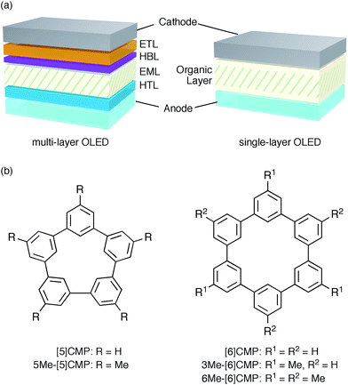 |
| | Fig. 1 Electrophosphorescent OLEDs. (a) Architectures of the electrophosphorescent OLEDs in the present study. The multi-layer OLED with a four-layer architecture possesses the following layer settings: cathode = LiF (0.5 nm)/Al (100 nm), ETL = Alq3 (20 nm), HBL = BAlq (10 nm), EML = 6 wt% Ir(ppy)3 in a host material (40 nm), HTL = α-NPD (20 nm), anode = PEDOT:PSS (30 nm)/ITO (110 nm). The single-layer OLED with a simple architecture possesses the following layer settings: cathode = Cs (1.5 nm)/Al (100 nm), organic layer = base material (10 nm)/6 wt% Ir(ppy)3 in base material (40 nm)/base material (10 nm), anode = PEDOT:PSS (30 nm)/ITO (110 nm). (b) Chemical structures of the CMPs. See Fig. S1† for the chemical structures of the other compounds. | |
A unique, potentially innovative architecture is currently being developed, i.e., a single-layer phosphorescent OLED (Fig. 1a).10–16 In the single-layer OLED, one base material is designed for multiple roles in the device and, with a phosphorescent emitter, can achieve nearly quantitative electro-optical conversion for the luminescence.10–12 In principle, the single-layer OLED simplifies the device with its simple architecture and the dramatically reduced tasks at the layer assembly stage. However, the present molecular designs of the base materials still rely on the conventional diode strategy and thus require substantial efforts in the synthesis of multiple elemental components, such as the donor or acceptor, and on the synthetic assembly thereof. Moreover, despite the synthetic efforts, the structural combination does not always succeed in the single-layer OLEDs with a high efficiency luminescence,13–16 partly because a guiding principle for the successful synthetic assembly is yet to be uncovered.
Revisiting aromatic hydrocarbons, we recently introduced a macrocyclization strategy for OLED materials.17–20 We demonstrated that electronically unbiased structures of hydrocarbons function as bipolar carrier transport materials for both electrons and holes. We envisioned that the bipolar characteristics of the aromatic hydrocarbons could be further developed into the multirole base materials in a single-layer OLED. We herein report our first effort on the design and synthesis of aromatic hydrocarbon macrocycle multirole base materials. A structure–performance relationship study revealed the particular importance of the steric design in the hydrocarbon materials. Expectedly, the steric design at the periphery was essential to controlling the packing structures in the devices, but, unexpectedly, the steric design at the macrocyclic core was also effective for preferentially tweaking the charge carrier mobility. As a result, one simple structural component of a hydrocarbon, i.e., toluene, was transformed into the single-component, multirole base material for the single-layer OLED with the utmost efficiency of electro-optical conversion. Furthermore, the versatility of the hydrocarbon base material was also demonstrated by its applicability to a white-light emitting OLED with three phosphorescent emitters. This study showed that the molecular design for the highly efficient single-layer OLED can depart from the conventional diode strategy and look more deeply into the wide bandgap structures of hydrocarbons, the very first origin of electroluminescent materials.1
Results and discussion
Molecular design for multirole materials in OLEDs
We started the molecular design of the aromatic hydrocarbon macrocycles from a screening study for the host materials in the EML. A remaining requisite for the aromatic hydrocarbon macrocycles as a multirole base material in the single-layer OLED was the applicability to host materials,17,18 which required a detour in the molecular design. Possessing electronically unbiased structures composed solely of hydrogen and carbon atoms, aromatic hydrocarbon macrocycles provide interesting and unique structural motifs that bear high thermal robustness and intrinsic bipolar charge transport abilities. Considering its smallest arylene units are benzene rings, we expected that the [n]cyclo-meta-phenylenes ([n]CMPs; Fig. 1b) should also function as host materials for phosphorescent emitters. However, although the [n]CMPs did indeed work as bipolar charge transport materials both for the HTL and ETL with the emission characteristics expected for multi-layer phosphorescent devices (Fig. 2),18 their performances as the host materials in typical multi-layer OLEDs were unexpectedly poor (Table 1). Thus, in an electrophosphorescent device using 6 wt% Ir(ppy)3 as the doped emitter (see also Fig. 1a), [5]- and [6]CMP exhibited negligible luminescence with EQE values of 0.0% (driving voltage (DV) = 3.1 V) and 1.0% (DV = 4.0 V), respectively, which are far inferior to the EQE value of 4.9% (DV = 5.2 V) for the standard material 4,4′-bis(N-carbazolyl)-1,1′-biphenyl (CBP). Throughout this study, all the organic thin films in the devices were deposited through sublimation, and the representative EQE values, after calibration with the angular distribution of the light, were sampled at 0.1 mA cm−2 for comparison. Other convertible measures of device performance, such as power efficiencies (PE) and current efficiencies (CE),9 are also shown as a reference.
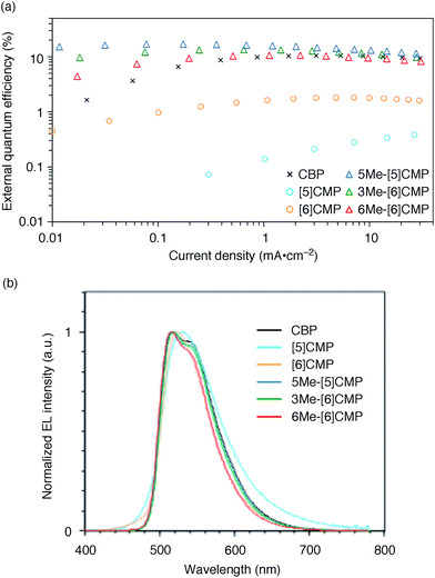 |
| | Fig. 2 Performance of the multi-layer OLEDs with various hosts. (a) External quantum efficiency plotted as a function of current density. See Fig. 1a for the device architecture. (b) Electroluminescence spectra at a current density of 0.1 mA cm−2. | |
Table 1 Representative performance data of the multi-layer phosphorescent OLEDsa
| Host material |
EQE (%) |
CE (cd A−1) |
PE (lm W−1) |
DV (V) |
|
Performances were evaluated at 0.1 mA cm−2, and the Lambertian factors for the data calibrations were as follows. For EQE: CBP = 0.99, [5]CMP = 1.18, [6]CMP = 0.91, 5Me-[5]CMP = 1.10, 3Me-[6]CMP = 1.04 and 6Me-[6]CMP = 0.99. For PE: CBP = 0.97, [5]CMP = 1.04, [6]CMP = 0.84, 5Me-[5]CMP = 1.10, 3Me-[6]CMP = 1.03 and 6Me-[6]CMP = 0.96.
|
| CBP |
4.9 |
17.7 |
10.2 |
5.2 |
| [5]CMP |
0.0 |
0.0 |
0.0 |
3.1 |
| [6]CMP |
1.0 |
3.7 |
2.5 |
4.0 |
| 5Me-[5]CMP |
16.8 |
55.1 |
31.2 |
6.1 |
| 3Me-[6]CMP |
12.3 |
43.1 |
27.5 |
5.1 |
| 6Me-[6]CMP |
7.9 |
29.2 |
15.6 |
5.6 |
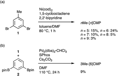
The molecular structures of the CMPs for the host materials were revised by taking into account the relevant physical properties. Although the poor performance of the [n]CMPs as the hosts in the OLED implied the leakage of the triplet-state excited energy of the Ir complex (vide supra), the solution-phase analysis of the [n]CMPs contrarily suggested their inherent potentials. Thus, the excited-state energy levels (ES and ET) for the singlet state (S1) and triplet state (T1) of the [n]CMPs in solution were high enough to accommodate the triplet-state energy of Ir(ppy)3 (2.4 eV) (Table 2).21 We therefore hypothesized that the crystalline characteristics in the deposited films resulted in the reduction of the excited-state energies of the CMPs.22 Theoretical calculations using the density functional theory (DFT) method indeed confirmed that the excited state energy (ES) of [6]CMP could be reduced by approximately 0.4 eV upon crystallization (Fig. 3). The introduction of methyl (Me) groups at the periphery of an [n]CMP was thus conceived to insulate the molecules from the π-orbital overlaps for high-ET host molecules, and a series of methylated congeners, mMe-[n]CMP (Fig. 1b), were designed by adopting concise synthesis methods. In short, 5Me-[5]CMP and 6Me-[6]CMP were synthesized from 3,5-dibromotoluene through our one-pot, Ni-mediated macrocyclization method,18,23 and 3Me-[6]CMP was synthesized via a newly developed cross-macrocyclization method using the Suzuki–Miyaura coupling reaction (Scheme 1) (see the Experimental section for further details).24
Table 2 Representative physical properties of the CMPs
|
|
T
d
(°C) |
E
S
(eV) |
E
T
(eV) |
|
The onset decomposition temperature Td was determined by thermogravimetric analysis on a TG-DTA2500 (Netzsch) after an equilibration time of 10 min at 40 °C with a heating rate of 10 °C min−1 in flowing helium.
The ES values were obtained from fluorescence spectra in chloroform at ambient temperature.
The ET values were obtained from phosphorescence spectra with excitation at the absorption maximum in 2-methyltetrahydrofuran at 77 K.
The data were acquired from a previous report.18
|
| [5]CMP |
358d |
3.52 |
2.73 |
| [6]CMP |
451d |
3.63 |
2.95 |
| 5Me-[5]CMP |
369 |
3.53 |
2.68 |
| 3Me-[6]CMP |
428 |
3.58 |
2.78 |
| 6Me-[6]CMP |
433 |
3.63 |
2.77 |
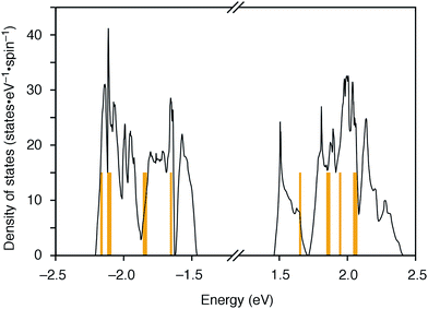 |
| | Fig. 3 DFT calculations of [6]CMP. Density of states of [6]CMP crystal (black lines) and the energy levels of an isolated [6]CMP molecule (orange lines). The energy differences between the valence top state and the conduction bottom state are 2.92 eV for the [6]CMP crystal and 3.30 eV for the [6]CMP molecule. The midgap energies are set to zero. | |
 |
| | Scheme 1 Synthesis of mMe-[n]CMP. (a) Synthesis of nMe-[n]CMP (n = 5–9) via a Yamamoto-type coupling reaction. (b) Synthesis of 3Me-[6]CMP via a Suzuki–Miyaura cross-coupling reaction. | |
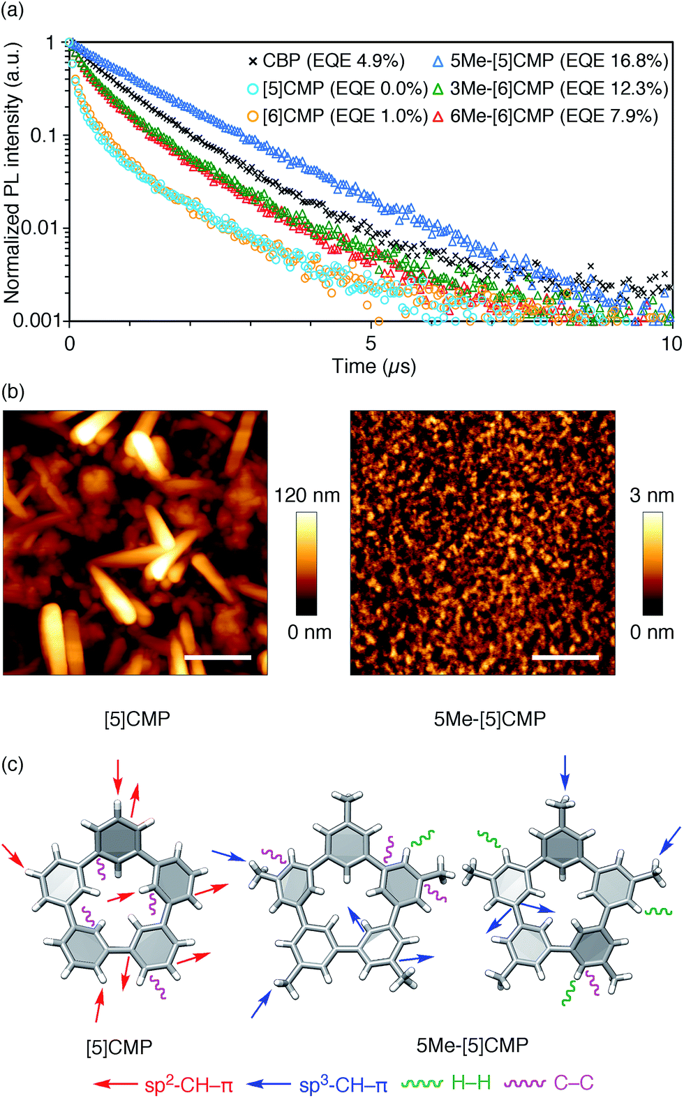
All three methylated congeners possessed preferable characteristics such as high-Td and high-ET values (Table 2) and worked well as the host materials in the multi-layer OLED with an Ir(ppy)3 emitter. Thus, the EQE values were dramatically improved to 16.8% (DV = 6.1 V), 12.3% (DV = 5.1 V) and 7.9% (DV = 5.6 V) for 5Me-[5]CMP, 3Me-[6]CMP and 6Me-[6]CMP, respectively (Fig. 2 and Table 1). All of the EQE values were superior to the value of 4.9% (DV = 5.2 V) for CBP. The photoluminescence decay of the Ir(ppy)3 in the mMe-[n]CMP layers confirmed a minute or negligible energy leakage in the thin films of these methylated hosts, and a comparison with those of the unsubstituted CMP molecules clearly showed an effective and favorable role of the methyl groups for the exciton confinement (Fig. 4a). Atomic-force microscopy (AFM) analysis supported our hypothesis of the crystalline characteristics of the unsubstituted congeners in thin films: the image of the [5]CMP film showed the presence of grains that were separated by boundaries of approximately 120 nm height,25 whereas the image of the 5Me-[5]CMP film revealed the presence of a smooth surface with a maximum deviation of 3 nm in height (Fig. 4b). The surface roughness was evaluated, and average Ra values of 18.5 nm for [5]CMP and 0.5 nm for 5Me-[5]CMP were obtained, which indicated the formation of an amorphous film for 5Me-[5]CMP.
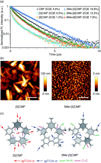 |
| | Fig. 4 Fundamental properties of the thin films. (a) Photoluminescence decay of Ir(ppy)3 (6 wt%) at 520 nm in a 40 nm thin film of the host materials with excitation at 335 nm. An identical layer was embedded as the EML in a four-layer OLED to yield the EQE values shown in the graph. See Fig. 2 and Table 1 for the details of the device performance. (b) AFM images of the thin films of [5]CMP (left) and 5Me-[5]CMP (right) deposited on a glass surface. The horizontal scale bars are 500 nm. (c) Molecular structures and intermolecular contacts of [5]CMP and 5Me-[5]CMP from X-ray diffraction analysis of single crystals. Two crystallographically inequivalent molecules of 5Me-[5]CMP are shown. See ESI† for data on the other compounds. | |
Structural information from an X-ray diffraction analysis of single crystals suggested that the differences in the thin film morphologies could be attributed to the differences in the intermolecular contacts. The sp2–CH–π contacts between the benzene rings predominated the intermolecular contacts in the [5]CMP crystal, whereas the sp2–CH–π contacts were diminished in the 5Me-[5]CMP crystal (Fig. 4c). Instead in the 5Me-[5]CMP crystal, various intermolecular contacts, such as sp3–CH–π, H–H and C–C contacts, appeared, which also resulted in two crystallographically inequivalent molecules per unit cell. Note that the rotational freedom of the methyl group can also compromise with the various relative orientations of the neighboring molecules in the solid.26 We believe that hampering the direct benzene–benzene contacts as well as increasing the variety of contacts and conformations preferentially contributed to the maintenance of the inherent high ET value of the methylated CMP in the thin film (Table 2).
Single-layer OLED
The single-layer architecture of the OLED was then examined with the hydrocarbon macrocycles, mMe-[n]CMPs. Despite the preceding studies with multi-component base materials,10–12 our investigations with the mMe-[n]CMPs showed that the donor–acceptor design is not a requisite for the highly efficient single-layer OLED. On the other hand, we revealed that the wide bandgap motif of the aromatic hydrocarbons is ideal for a multirole, single-component base material and found a requisite property to realize a highly efficient single-layer OLED. We first fabricated a single-layer OLED with CBP as a reference. The single-layer OLED of CBP with 6 wt% of Ir(ppy)3 (Fig. 1a) emitted electroluminescence with an EQE value of 4.9% (DV = 3.3 V; Fig. 5 and Table 3). The EQE values of 5.3% (DV = 4.8 V) for 6Me-[6]CMP and 7.3% (DV = 4.5 V) for 3Me-[6]CMP with the single-layer architecture containing the doped Ir(ppy)3 emitter were close to the level of CBP and this was not surprising (Fig. 5 and Table 3). However, the EQE value of 22.8% (DV = 5.7 V) recorded for 5Me-[5]CMP was unexpected. The EQE value was even close to the highest values of preceding OLEDs with Ir emitters (20–30%) embedded in the materials with donor–acceptor diode designs.4–10 To the best of our knowledge, among the multi-component base materials, there exists only one example of a single-layer OLED achieving a higher electro-optical conversion (EQE = 26.8%)10 which is comparable to the level of the state-of-the-art multi-layer OLEDs.4–9,27 An estimate of the light out-coupling efficiency of 20–30% (ref. 6, 7 and 28) indicated that nearly quantitative electro-optical conversion with an internal quantum efficiency in the range of 100–76% was achieved in the single-layer OLED with the aromatic hydrocarbon material, 5Me-[5]CMP.
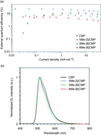 |
| | Fig. 5 Performance of the single-layer OLED. (a) External quantum efficiency of the single-layer OLED plotted against the current density. See Fig. 1a for the device architecture. (b) Electroluminescence spectra at a current density of 0.1 mA cm−2. | |
Table 3 Representative performance data of the single-layer phosphorescent OLEDsa
| Base material |
EQE (%) |
CE (cd A−1) |
PE (lm W−1) |
DV (V) |
|
Performances were evaluated at 0.1 mA cm−2, and the Lambertian factors for the data calibrations were as follows. For EQE: CBP = 1.80, 5Me-[5]CMP = 0.87, 3Me-[6]CMP = 0.81, 6Me-[6]CMP = 0.87. For PE: CBP = 1.56, 5Me-[5]CMP = 0.84, 3Me-[6]CMP = 0.81, 6Me-[6]CMP = 0.90.
|
| CBP |
4.9 |
9.5 |
14.0 |
3.3 |
| 5Me-[5]CMP |
22.8 |
94.1 |
43.5 |
5.7 |
| 3Me-[6]CMP |
7.3 |
30.1 |
17.3 |
4.5 |
| 6Me-[6]CMP |
5.3 |
21.7 |
11.4 |
4.8 |
Although we do not fully understand the requisite for the multirole hydrocarbons in the single-layer OLED at this stage, we observed one important and anomalous characteristic of 5Me-[5]CMP in comparison with the other mMe-[n]CMPs. The fundamental energetics in the devices were commonly shared among the CMPs as well as CBP (Fig. 6). However, one peculiar behavior of 5Me-[5]CMP was observed in the J–V characteristics of the hole-only and electron-only devices (HODs and EODs; Fig. 7).11,12 The driving voltage for 100 mA cm−2 of the hole current density in the HOD was particularly increased by 18.1 V (from 9.4 V to 27.5 V) upon doping the layer of 5Me-[5]CMP with 6 wt% of Ir(ppy)3, whereas the increases from the doping of the layers of other materials, i.e., 3Me- and 6Me-[6]CMP, were much smaller (<6 V, Fig. 7). An increase of the driving voltage in the EOD for 100 mA cm−2 electron current densities was negligible for all of the materials (<4 V). When the J–V characteristics were interpreted in terms of the charge carrier mobilities through the application of Child's law at the same current density,11,12 we observed that the doping of Ir(ppy)3 resulted in marked and peculiar retardation of the hole mobility in the 5Me-[5]CMP layer (2.2 × 10⁻⁵vs. 9.3 × 10⁻⁷ cm2 V−1 s−1; Table 4). We believe that the hole retarding effect of the dopant in the 5Me-[5]CMP layer preferentially operated to confine the charge recombination site around the doped region and functioned similarly to the HBL. Preceding studies on Ir(ppy)3 revealed that the emitter can act as a hole trap at the charge recombination step,12,29 and the effective transfer of the hole to the emitter, which was observed particularly with 5Me-[5]CMP in our case, should be favorable for highly efficient electroluminescence. This result shows that, in addition to high ET values,20 a subtle control over the charge mobilities is a requisite for the molecular design of the single-layer OLED.
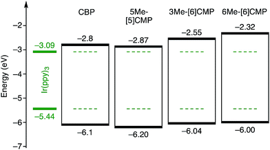 |
| | Fig. 6 Energetics of the single-layer OLED. All the base materials possessed similar energetics especially in the HOMO levels. The HOMO levels were directly measured by photo-electron spectroscopy in air (PESA), and the LUMO levels were estimated using the optical energy gaps obtained from the absorbance onsets of the thin films. The data for CBP were acquired from the literature.8 | |
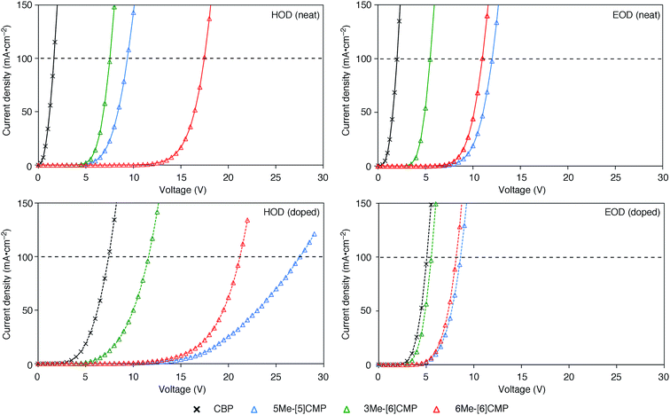 |
| | Fig. 7
J–V characteristics of the HOD and EOD are shown for the devices in the absence (neat) or presence (doped) of Ir(ppy)3 (6 wt%). The horizontal broken line shows 100 mA cm−2. The HOD device was assembled with an ITO (110 nm)/PEDOT:PSS (30 nm)/organic layer (60 nm)/α-NPD (20 nm)/Al (100 nm) architecture, and the EOD device was assembled with an ITO (110 nm)/PEDOT:PSS (30 nm)/Ca (5 nm)/organic layer (60 nm)/Cs (1.5 nm)/Al (100 nm) architecture. The organic layer was composed either of a single material (neat) or a material containing 6 wt% Ir(ppy)3 dopant (doped). | |
Table 4 Mobility data of the HOD and EODa
| Base material |
μ (cm2 V−1 s−1) (neat) |
μ (cm2 V−1 s−1) (doped) |
| Hole |
Electron |
Hole |
Electron |
|
The mobilities were estimated at 100 mA cm−2 from J–V2 characteristics using Child's law (J = 9εμV2/8L3) for the neat layers and doped layers.
|
| CBP |
2.1 × 10⁻⁴ |
1.9 × 10⁻⁴ |
2.3 × 10⁻⁵ |
6.8 × 10⁻⁵ |
| 5Me-[5]CMP |
2.2 × 10⁻⁵ |
2.0 × 10⁻⁵ |
9.3 × 10⁻⁷ |
2.5 × 10⁻⁵ |
| 3Me-[6]CMP |
4.4 × 10⁻⁵ |
6.0 × 10⁻⁵ |
1.2 × 10⁻⁵ |
6.7 × 10⁻⁵ |
| 6Me-[6]CMP |
1.1 × 10⁻⁵ |
2.4 × 10⁻⁵ |
6.7 × 10⁻⁶ |
3.2 × 10⁻⁵ |
The key structural features of the hydrocarbon base materials were thus deduced as follows: (1) unbiased hydrocarbon motifs for the bipolar charge transport, (2) macrocyclic structures for the high thermal robustness, (3) transparency in the visible light region (vide infra), (4) steric design of the periphery to hamper the direct π–π contacts for the high-ET base materials and (5) steric design of the macrocyclic core for the induction of the hole retarding effect with the emitter. To deduce the origin of the last feature, the hole retarding effect, more clearly, we compared 5Me-[5]CMP and the mMe-[6]CMPs in detail. These molecules share substantially similar characteristics and structural features: they have bipolar transport activities, high thermal robustness, high-ET values and preferable energetics in the device (Table 2 and Fig. 6) and, consequently, perform comparably as the host in the multi-layer architecture (vide supra). We thus concluded that the last requisite of the retarding effect should have a structural origin and, after examining several structural features, we noted the conformational flexibilities of the macrocyclic cores were the most probable candidate. As shown in Fig. 8, the energy barriers examined for a dihedral angle at the single-bond linkages were different between 5Me-[5]CMP and 6Me-[6]CMP.30 The energy barrier for one phenylene panel to pass through the macrocyclic pore (dihedral angle = 0°) was 0.6 kcal mol−1 for 5Me-[5]CMP and 3.8 kcal mol−1 for 6Me-[6]CMP. In addition, this phenylene rotation for 5Me-[5]CMP accompanied larger structural deviations than those for 6Me-[6]CMP. We can thus expect that 5Me-[5]CMP flexibly adopts various conformations and, upon doping with the emitter, increases the intermolecular contacts to accommodate the emitter preferably.
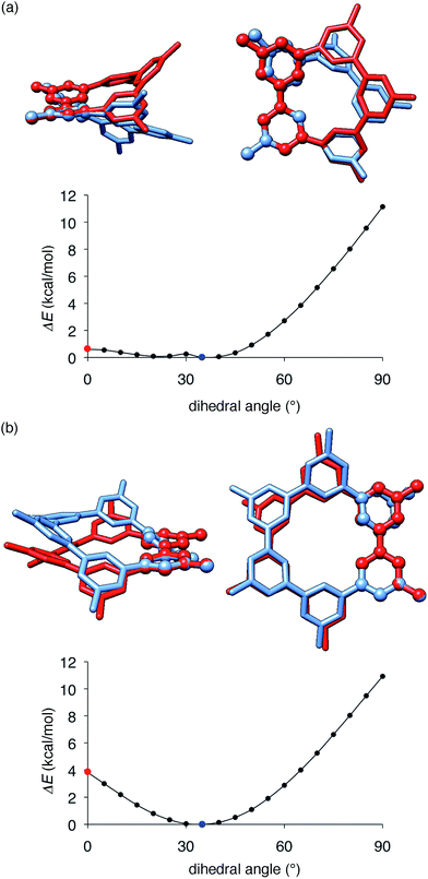 |
| | Fig. 8 Structures and energetics for the rotation of one phenylene panel. A dihedral angle at the phenylene–phenylene linkages shown with ball-and-stick models was constrained and rotated by 5°. At each constrained point, the most stable structure was obtained by low-mode conformational search calculations (1000 steps) with the MM3* force field (MacroModel), and the energy was obtained by single-point DFT calculations with B3LYP/6-31G(d,p) (Gaussian). The global minima at 35° are shown in blue, and the high energy conformers at 0° are shown in red. The structures were overlaid by minimizing the root-mean-square deviation of the atomic positions (RMSD) of one reference phenylene panel. (a) 5Me-[5]CMP. RMSD for all of the atoms was 1.633 Å. (b) 6Me-[6]CMP. RMSD for all of the atoms was 0.859 Å. | |
We finally examined the scope of the single-layer architecture for multiple phosphorescent emitters. Note that the aromatic hydrocarbon macrocycles possess an ideally wide window for optoelectronic applications with absorption edges appearing at relatively shorter wavelengths for conjugated π-systems, which is another key feature of conjugated macrocycles. As a result of the wide gap between the HOMO and the LUMO (Fig. S2 and Table S1†),17,18 the absorption edges of CMP were observed around 300 nm (Fig. S3†). The absorption is, for instance, much shorter than the 350–400 nm of the CBP derivatives. We then assembled a white-light-emitting single-layer OLED31,32 using a blend of three different phosphorescent emitters, i.e., fac-Ir(mpim)3 for blue,33 Ir(ppy)3 for green5 and Ir(piq)3 for red,34 albeit preliminary with an identical architecture as the green device. The device emitted a white light with Commission Internationale de l'Eclairage (CIE) coordinates of (0.30, 0.44) and an EQE value of 10.4% (Fig. 9). The results demonstrated the feasibility of full-color tunings in single-layer OLEDs with aromatic hydrocarbons.
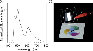 |
| | Fig. 9 White OLED with a single-layer architecture. (a) An electroluminescence spectrum at a current density of 0.1 mA cm−2. (b) A picture of the device with an emitting area of 16.6 mm × 6 mm. The sheet under the device is showing a color reference printed on white paper, and the original colors can be found at http://www.jst.go.jp/erato/isobe/. | |
Conclusion
We demonstrated that a single, very simple hydrocarbon motif of toluene can be utilized, upon macrocyclization, as the multirole base material of a single-layer OLED. The electro-optical conversion in the simplified device reaches a level comparable to the state-of-the-art multi-layer OLEDs, which shows the benefit of the wide bandgap hydrocarbon motifs for the design of multirole base materials. The overall fabrication processes of the OLEDs were thus substantially simplified from the synthetic stage at the bottom through the one-pot macrocyclization strategy. The molecular design using macrocyclization needs to be supplemented by the steric design to cover all of the elemental roles such as the bipolar charge carrier transport and the high ET values, and this new guiding principle should be fully explored and developed in the future. The structural chemistry of the aromatic hydrocarbon macrocycles is currently being enriched by structural variants and may further stimulate exploration.35–37 A peculiar hole retarding effect of the phosphorescent emitter was observed only in the most successful layer composed of 5Me-[5]CMP, which implied the importance of conformational flexibility for the preferential accommodation of the emitter. The preceding examples of spiro-structured aromatic hydrocarbons for the host materials may, albeit unintentionally, have utilized similar molecular recognition with the emitter at their concave sites.38 The versatility of the multirole hydrocarbon materials should also be exploited for other efficient emitters and may be examined, for instance, with those using thermally assisted delayed fluorescence in the future.28 The future investigations should involve subtle electronic tuning of the periphery moieties for further improvements of device performance such as the driving voltage.
Experimental section
Theoretical calculations at the solid state
DFT calculations were performed within the generalized-gradient approximation using the quantum-ESPRESSO code.39 We employed the exchange-correlation potential with the Perdew–Burke–Ernzerhof parameterization.40 Ultrasoft pseudopotentials41 plain-wave basis sets with cutoff energies of 30 Ry for wave functions and 150 Ry for charge densities and a 1 × 1 × 1 k-point mesh were used.
Synthesis
Fully methylated macrocycles, nMe-[n]CMPs, were synthesized from 3,5-dibromotoluene (10.2 g, 40.8 mmol) by a Ni-mediated macrocyclization reaction.18 The yields were 15% (n = 5; 567 mg, 1.26 mmol), 24% (n = 6; 1.05 g, 1.61 mmol), 10% (n = 7; 362 mg, 0.570 mmol), 5% (n = 8; 205 mg, 0.239 mmol) and 3% (n = 9; 100 mg, 0.123 mmol). A partially methylated macrocycle, 3Me-[6]CMP, was synthesized as follows. A mixture of 3,5-dibromotoluene (2.50 g, 10.0 mmol), 1,3-benzenediboronic acid bis(pinacol) ester (3.30 g, 10.0 mmol), tris(dibenzylideneacetone)dipalladium(0)-chloroform adduct (512 mg, 0.495 mmol), 2-dicyclohexylphosphino-2′,6′-dimethoxybiphenyl (801 mg, 1.95 mmol) and cesium carbonate (16.3 g, 50.0 mmol) in degassed, dry DMF (1.0 L) was stirred at 110 °C for 24 h in a glovebox under nitrogen atmosphere. The reaction mixture was brought outside the glovebox, and water (700 mL) was added. The resulting precipitates were collected by filtration, washed with methanol (10 mL) and dried under vacuum. The solid was extracted with chloroform (200 mL), and the solution was dried with magnesium sulfate and concentrated under vacuum. The crude material was then purified by silica gel column chromatography with a chloroform eluent, by GPC and by washing with 50% methanol/chloroform (7 mL) to afford 3Me-[6]CMP as a white powder in a 9% yield (150 mg, 0.300 mmol).
Device
Phosphorescent organic light-emitting diode devices were prepared and evaluated as we reported previously.18
X-ray analysis
Single crystals for nMe-[n]CMP (n = 5–9) and 3Me-[6]CMP were obtained as described in the synthesis methods and analyzed by X-ray diffraction. The single crystals were mounted on a thin polymer tip with cryoprotectant oil and frozen at the measurement temperature with flash-cooling. The diffraction data were collected and processed with Rigaku CrystalClear software42 or the HKL2000 software program.43 The structure was solved by direct methods using a charge flipping method44 or SHELXS45 and refined by full-matrix least-squares on F2 using the SHELX program suite44 running on the Rigaku CrystalStructure software program46 or the Yadokari-XG 2009 software program.47 Geometrical restraints on the disordering solvent molecules, i.e., DFIX, DANG, SIMU and ISOR, were used in the refinements. The non-hydrogen atoms were analyzed anisotropically, and the hydrogen atoms were input at calculated positions and refined with a riding model.
Theoretical calculations on the conformational flexibility
The conformational flexibility of the CMPs was analyzed by a protocol that we used for the analysis of cyclophanes.30 Thus, a dihedral angle at the phenylene–phenylene linkages was constrained and rotated by 5°. At each constrained point, the most stable structure was obtained by low-mode conformational search calculations (1000 steps) with the MM3* force field (MacroModel, Maestro v9.8),48 and the energy was obtained by single-point DFT calculations with B3LYP/6-31G(d,p) (Gaussian09).49
Acknowledgements
This work was partly supported KAKENHI (24241036, 25107708, 25102007). We thank Mr H. Kiso for his help in the device fabrications and SPring-8 (Research 2014B2016) for the use of the X-ray diffraction instruments.
Notes and references
- W. Helfrich and W. G. Schneider, Phys. Rev. Lett., 1965, 14, 229–231 CrossRef CAS
 .
.
- P. S. Vincett, W. A. Barlow, R. A. Hann and G. G. Roberts, Thin Solid Films, 1982, 94, 171–183 CrossRef CAS .
- C. W. Tang and S. A. VanSlyke, Appl. Phys. Lett., 1987, 51, 913–915 CrossRef CAS .
- M. A. Baldo, D. F. O'Brien, Y. You, A. Shoustikov, S. Sibley, M. E. Thompson and S. R. Forrest, Nature, 1998, 395, 151–154 CrossRef CAS .
- M. A. Baldo, S. Lamansky, P. E. Burrows, M. E. Thompson and S. R. Forrest, Appl. Phys. Lett., 1999, 75, 4–6 CrossRef CAS .
- D. Tanaka, H. Sasabe, Y.-J. Li, S.-J. Su, T. Takeda and J. Kido, Jpn. J. Appl. Phys., 2007, 46, L10–L12 CrossRef CAS .
- L. H. Smith, J. A. E. Wasey and W. L. Barnes, Appl. Phys. Lett., 2004, 84, 2986–2988 CrossRef CAS .
- V. I. Adamovich, S. R. Cordero, P. I. Djurovich, A. Tamayo, M. E. Thompson, B. W. D'Andrade and S. R. Forrest, Org. Electron., 2003, 4, 77–87 CrossRef CAS .
- B. Minaev, G. Baryshnikov and H. Agren, Phys. Chem. Chem. Phys., 2014, 16, 1719–1758 RSC .
- Z. M. Hudson, Z. Wang, M. G. Helander, Z.-H. Lu and S. Wang, Adv. Mater., 2012, 24, 2922–2928 CrossRef CAS PubMed .
- C. Cai, S.-J. Su, T. Chiba, H. Sasabe, Y.-J. Pu, K. Nakayama and J. Kido, Org. Electron., 2011, 12, 843–850 CrossRef CAS .
- X. Qiao, Y. Tao, Q. Wang, D. Ma, C. Yang, L. Wang, J. Qin and F. Wang, J. Appl. Phys., 2010, 108, 034508 CrossRef .
- J. Ye, Z. Chen, K. Wang, F. An, Y. Yuan, W. Chen, Q. Yang, X. Zhang and C.-S. Lee, Chem.–Eur. J., 2014, 20, 13762–13769 CrossRef CAS PubMed .
- C.-H. Chen, W.-S. Huang, M.-Y. Lai, W.-C. Tsao, J. T. Lin, Y.-H. Wu, T.-H. Ke, L.-Y. Chen and C.-C. Wu, Adv. Funct. Mater., 2009, 19, 2661–2670 CrossRef CAS .
- H. Tsuji, C. Mitsui, Y. Sato and E. Nakamura, Adv. Mater., 2009, 21, 3776–3779 CrossRef CAS .
- J. P. J. Markham, S.-C. Lo, S. W. Magennis, P. L. Burn and I. D. W. Samuel, Appl. Phys. Lett., 2002, 80, 2645–2647 CrossRef CAS .
- W. Nakanishi, T. Yoshioka, H. Taka, J. Y. Xue, H. Kita and H. Isobe, Angew. Chem., Int. Ed., 2011, 50, 5323–5326 CrossRef CAS PubMed .
- J. Y. Xue, K. Ikemoto, N. Takahashi, T. Izumi, H. Taka, H. Kita, S. Sato and H. Isobe, J. Org. Chem., 2014, 79, 9735–9739 CrossRef CAS PubMed .
- W. Nakanishi, S. Hitosugi, A. Piskareva, Y. Shimada, H. Taka, H. Kita and H. Isobe, Angew. Chem., Int. Ed., 2010, 49, 7239–7242 CrossRef CAS PubMed .
- W. Nakanishi, Y. Shimada, H. Taka, H. Kita and H. Isobe, Org. Lett., 2012, 14, 1636–1639 CrossRef CAS PubMed .
- K. Goushi, R. Kwong, J. J. Brown, H. Sasabe and C. Adachi, J. Appl. Phys., 2004, 95, 7798–7802 CrossRef CAS .
- J. L. Brédas, J. P. Calbert, D. A. da Silva Filho and J. Cornil, Proc. Natl. Acad. Sci. U. S. A., 2002, 99, 5804–5809 CrossRef PubMed .
- H. Bräunling, F. Binnig and H. A. Staab, Chem. Ber., 1967, 100, 880–888 CrossRef .
- N. Miyaura and A. Suzuki, Chem. Rev., 1995, 95, 2457–2483 CrossRef CAS .
- H. Yang, T. J. Shin, M.-M. Ling, K. Cho, C. Y. Ryu and Z. Bao, J. Am. Chem. Soc., 2005, 127, 11542–11543 CrossRef CAS PubMed .
- O. Takahashi, Y. Kohno and M. Nishio, Chem. Rev., 2010, 110, 6049–6076 CrossRef CAS PubMed .
- The PE or CE values depend on the eye-sensitivity, and we thus did not directly compare the values in our study. Nonetheless, due to a preferable directionality of emitting light, the CE value of 94.1 cd A−1 for our hydrocarbon single-layer architecture recorded the highest values for single-layer OLEDs (see also ref. 10).
- H. Uoyama, K. Goushi, K. Shizu, H. Nomura and C. Adachi, Nature, 2012, 492, 234–238 CrossRef CAS PubMed .
- N. Matsusue, S. Ikame, Y. Suzuki and H. Naito, Appl. Phys. Lett., 2004, 85, 4046–4048 CrossRef CAS .
- W. Nakanishi, Y. Shimada and H. Isobe, Chem.–Asian J., 2013, 8, 1177–1181 CrossRef CAS PubMed .
- J. Kido, M. Kimura and K. Nagai, Science, 1995, 267, 1332–1334 CrossRef CAS PubMed .
- M. C. Gather, A. Köhnen and K. Meerholz, Adv. Mater., 2011, 23, 233–248 CrossRef CAS PubMed .
- K. Udagawa, H. Sasabe, C. Cai and J. Kido, Adv. Mater., 2014, 26, 5062–5066 CrossRef CAS PubMed .
- A. Tsuboyama, H. Iwawaki, M. Furugori, T. Mukaide, J. Kamatani, S. Igawa, T. Moriyama, S. Miura, T. Takiguchi, S. Okada, M. Hoshino and K. Ueno, J. Am. Chem. Soc., 2003, 125, 12971–12979 CrossRef CAS PubMed .
- M. Iyoda, J. Yamakawa and M. J. Rahman, Angew. Chem., Int. Ed., 2011, 50, 10522–10553 CrossRef CAS PubMed .
- S. E. Lewis, Chem. Soc. Rev., 2015, 44, 2221–2304 RSC .
- T. Matsuno, H. Naito, S. Hitosugi, S. Sato, M. Kotani and H. Isobe, Pure Appl. Chem., 2014, 86, 489–495 CrossRef CAS .
- K.-T. Wong, Y.-L. Liao, Y.-T. Lin, H.-C. Su and C.-C. Wu, Org. Lett., 2005, 7, 5131–5134 CrossRef CAS PubMed .
- P. Giannozzi, S. Baroni, N. Bonini, M. Calandra, R. Car, C. Cavazzoni, D. Ceresoli, G. L. Chiarotti, M. Cococcioni, I. Dabo, A. D. Corso, S. de Gironcoli, S. Fabris, G. Fratesi, R. Gebauer, U. Gerstmann, C. Gougoussis, A. Kokalj, M. Lazzeri, L. Martin-Samos, N. Marzari, F. Mauri, R. Mazzarello, S. Paolini, A. Pasquarello, L. Paulatto, C. Sbraccia, S. Scandolo, G. Sclauzero, A. P. Seitsonen, A. Smogunov, P. Umari and R. M. Wentzcovitch, J. Phys.: Condens. Matter, 2009, 21, 395502 CrossRef PubMed .
- J. P. Perdew, K. Burke and M. Ernzerhof, Phys. Rev. Lett., 1996, 77, 3865–3868 CrossRef CAS PubMed .
- D. Vanderbilt, Phys. Rev. B: Condens. Matter Mater. Phys., 1990, 41, 7892–7895 CrossRef .
-
CrystalClear-SM Expert 2.1 b29, Rigaku Corporation, Tokyo, Japan, 2013 Search PubMed .
-
Z. Otwinowski and W. Minor, Methods in Enzymology, Part A, Macromolecular Crystallography, Academic, New York, 1997, vol. 276, pp. 307–326 Search PubMed .
- L. Palatinus and G. Chapuis, J. Appl. Crystallogr., 2007, 40, 786–790 CrossRef CAS .
- G. M. Sheldrick, Acta Crystallogr., Sect. A: Found. Crystallogr., 2008, 64, 112–122 CrossRef CAS PubMed .
-
CrystalStructure 4.1, Rigaku Corporation, Tokyo, Japan, 2014 Search PubMed .
- C. Kabuto, S. Akine, T. Nemoto and E. Kwon, J. Crystallogr. Soc. Jpn., 2009, 51, 218–224 CrossRef .
-
Maestro v.9.8, Schrödinger, New York, U.S.A., 2014 Search PubMed .
-
M. J. Frisch, G. W. Trucks, H. B. Schlegel, G. E. Scuseria, M. A. Robb, J. R. Cheeseman, G. Scalmani, V. Barone, B. Mennucci, G. A. Petersson, H. Nakatsuji, M. Caricato, X. Li, H. P. Hratchian, A. F. Izmaylov, J. Bloino, G. Zheng, J. L. Sonnenberg, M. Hada, M. Ehara, K. Toyota, R. Fukuda, J. Hasegawa, M. Ishida, T. Nakajima, Y. Honda, O. Kitao, H. Nakai, T. Vreven, J. A. Montgomery Jr, J. E. Peralta, F. Ogliaro, M. Bearpark, J. J. Heyd, E. Brothers, K. N. Kudin, V. N. Staroverov, R. Kobayashi, J. Normand, K. Raghavachari, A. Rendell, J. C. Burant, S. S. Iyengar, J. Tomasi, M. Cossi, N. Rega, J. M. Millam, M. Klene, J. E. Knox, J. B. Cross, V. Bakken, C. Adamo, J. Jaramillo, R. Gomperts, R. E. Stratmann, O. Yazyev, A. J. Austin, R. Cammi, C. Pomelli, J. W. Ochterski, R. L. Martin, K. Morokuma, V. G. Zakrzewski, G. A. Voth, P. Salvador, J. J. Dannenberg, S. Dapprich, A. D. Daniels, Ö. Farkas, J. B. Foresman, J. V. Ortiz, J. Cioslowski and D. J. Fox, Gaussian 09, Revision D.01, Gaussian, Inc., Wallingford CT, U.S.A., 2009 Search PubMed .
Footnote |
| † Electronic supplementary information (ESI) available: Supplementary data and methods. CCDC 1054912–1054917. For ESI and crystallographic data in CIF or other electronic format see DOI: 10.1039/c5sc03807c |
|
| This journal is © The Royal Society of Chemistry 2016 |

 Open Access Article
 This Open Access Article is licensed under a Creative Commons Attribution-Non Commercial 3.0 Unported Licence
 *abc
*abc