
Thiol-capped CdTe quantum dots hosted in saponites
Elena Pérez-Barrado†
 abc,
Lluís F. Marsalc,
Magdalena Aguilób,
Yolanda Cesterosa,
Francesc Díazb,
Josep Pallarèsc,
Fabio Cucinotta‡
d,
Leonardo Marchesed,
Maria Cinta Pujolb and
Pilar Salagre*a
abc,
Lluís F. Marsalc,
Magdalena Aguilób,
Yolanda Cesterosa,
Francesc Díazb,
Josep Pallarèsc,
Fabio Cucinotta‡
d,
Leonardo Marchesed,
Maria Cinta Pujolb and
Pilar Salagre*a
aDept. Química Física i Inorgànica, EMAS, Univ. Rovira i Virgili (URV), Marcel lí Domingo 1, E-43007 Tarragona, Spain. E-mail: pilar.salagre@urv.cat
bFísica i Cristal lografia de Materials i Nanomaterials (FICMA-FiCNA), EMAS, Univ. Rovira i Virgili (URV), Marcel lí Domingo 1, E-43007 Tarragona, Spain
cDept. d'Enginyeria Electrònica, Elèctrica i Automàtica, EMAS, Univ. Rovira i Virgili (URV), Avda. Països Catalans 26, E-43007 Tarragona, Spain
dDipartimento di Scienze e Tecnologie Avanzate, Centro Interdisciplinare Nano-Sistemi, Università del Piemonte Orientale “Amedeo Avogadro”, Viale T. Michel 11, 15121 Alessandria, Italy
First published on 26th October 2016
Abstract
Composite materials were easily prepared based on saponites where thiol-capped CdTe quantum dots (QDs) were hosted. A saponite was exchanged with a cationic polyelectrolyte solution of poly(diallyldimethylammonium chloride) (PDDA) and the thiol-capped QDs. Two composites based on delaminated saponites, a cationic polyelectrolyte and CdTe QDs were also prepared by spin-coating on a glass support. The presence of the QDs hosted in the inorganic matrices was tested by FT-IR and optical luminescence measurements. Additionally, a light-emitting diode was assembled and its I–V electrical characteristics are presented. Transition from ohmic behaviour to space charge limited conduction appeared at a turn-on voltage of 5.2 V.
Introduction
Quantum dots (QDs) are semiconductor nanoparticles with interesting properties: sharp emission spectra, strong brightness, high photostability, high absorption coefficients and high luminescent efficiency, amongst many others. The spectral properties can be controlled by variation of the particle size. They usually range in size between 1 and 10 nm.1–3 Much of the growing interest regarding QDs relies in nanotechnology applications. In the field of medicine, QDs are used for biosensing, gene and drug delivery (in functionalized form) and for bioimaging.3–7 QDs may be used as light harvesters for the assembly of solar cells8–10 and, also, as luminescent dopants for light emitting diodes (LEDs).11–13 Another field of interest is the design of catalysts with enhanced photocatalytic activity, which is being widely investigated.14 Because of the unique properties and potential applications of QDs in the above mentioned fields, current research is also focused on the synthesis of materials with luminescent properties where the QDs are embedded and/or hosted, in inorganic matrixes or in layer-by-layer (LbL) assemblies.15 Thus, aiming at the application in optoelectronic devices, as well as in the field of bioimaging, it is required to have the QDs as solid samples rather than in colloidal suspension, without altering the photostability of these semiconductor nanoparticles. QDs deposited in films have potential applications in the fields of sensors and photocatalysis as 2D architectures.16,17The presence of QDs in solid matrices aims at producing composite materials with high brightness, long-term stability, avoidance of QD aggregation and QD quenching, amongst others.18 The dispersion of QDs in clay mineral materials is already reported in the literature.19–24 Clay minerals are used as inorganic hosts due to their unique properties: large surface area, swelling behaviour, stability and biocompatibility.22 Saponites are common clays of the mineral group smectite. They have theoretical formula [Si8−xAlx]T[Mg62+]oO20(OH)4 [Mx+]·nH2O and can be synthesized using different procedures.25,26 QD composites synthesized by LbL assembly are mentioned in published literature. In order to stabilize the QD 2D films, films of clay minerals, and polyelectrolytes are used. Because of the potential applications of these 2D nanocomposite materials in solid state devices, some architectures have been studied.27–30 The addition of a polyelectrolyte constituted by bulky cations in these LbL assemblies is quite common as it acts as an inorganic cluster for introducing negatively-charged nanoparticles.31–34
In this work, we report on the facile synthesis of composite luminescent materials that are potential candidates for nanotechnology applications. These materials are based on saponites as inorganic matrices for hosting thiol-capped CdTe QDs (hereafter CdTe). Additionally, saponite/polyelectrolyte/CdTe composites were also synthesized as a LbL assembly by spin-coating. The polyelectrolyte used was poly(diallyldimethylammonium chloride) (hereafter PDDA). In addition, a light emitting diode was assembled and its electrical characteristics tested with saponite/PDDA/CdTe architecture as emissive layer.
Experimental
Synthesis of CdTe–saponites
The synthesis of a delaminated saponite was done following a procedure previously published.35 The hydrothermal treatment was done by the use of microwave irradiation at 453 K for 6 h. The sample was recovered by filtration and dried in an oven overnight at 353 K. This sample was called dS.The process for intercalation of the CdTe QDs was done similarly to a procedure reported before but with some modifications.36 The sample was synthesized by exchanging 0.5 g of delaminated saponite with 5 g of PDDA solution (20 wt% in H2O, Sigma-Aldrich). The exchange was done by adding 5 g of the PDDA under stirring at room temperature for 24 h. The exchanged clay, named afterwards dSPDDA, was recovered by centrifugation at 8000 rpm for 8 min (repeated twice). Then it was diluted in 100 ml of deionized water and stirred for 5 min. A portion of 30 g was transferred to a small beaker, where 200 μl of the CdTe QDs solution (1 × 10⁻⁵ M) were added (kindly provided by Prof. A. Eychmüller, Technische Universität Dresden). The CdTe QDs were capped with thioglycolic acid. The solution was left overnight with agitation. Then, the solid was recovered by centrifugation at 7000 rpm for 10 min (repeated twice). The recovered solid was dried overnight at 333 K. This sample was named as CdTe–dSPDDA.
Assembly of the composites dS/PDDA/CdTe and dSPDDA/CdTe
The first composite dS/PDDA/CdTe was assembled on a glass substrate, previously thoroughly cleaned, by spin coating (using a POLOS, model SPIN200I, spin-coater) the dS (2 mg ml−1 in ethanol) and PDDA (6.6 wt% in Milli-Q water) solutions as follows: dS film (spin coating program: 1st step at 500 rpm for 10 s and 2nd step at 1000 rpm for 90 s) and PDDA film (spin-coating program: 1st step at 500 rpm for 10 s and 2nd step at 1000 rpm for 90 s). The CdTe QDs (0.2 × 10⁻⁵ M in Milli-Q water) were finally deposited by drop-casting the CdTe QDS solution.The second composite dSPDDA/CdTe was assembled on a glass substrate, which was thoroughly cleaned by spin coating the dSPDDA solution (delaminated saponite exchanged with PDDA, synthesis procedure described in previous section, 2 mg ml−1 in ethanol) (spin coating program: 1st step at 500 rpm for 10 s and 2nd step at 1000 rpm at 90 s). The CdTe QDs (0.2 × 10⁻⁵ M in Milli-Q water) were deposited by drop-casting.
Assembly of a light-emitting diode with architecture ITO/PEDOT:PSS/(dS/PDDA/CdTe)6/Au/Ag
The assembly of the LED was done as follows. First, a glass substrate with the patterned ITO (indium tin oxide) was thoroughly cleaned with soap, acetone, ethanol and Milli-Q water. All spin-coated films were deposited using a 0.20 μm filter (Sartorius) attached to a 1 ml-syringe. A film of PEDOT:PSS (poly(3,4-ethylenedioxythiophene)-poly(styrenesulfonate)) was deposited by spin coating (spin coating program: 2500 rpm for 50 s) and afterwards it was heated at 393 K for 20 min. Then, a film of dS (5 mg ml−1 in ethanol) was spin-coated (spin coating program: 1000 rpm for 60 s), a film of PDDA (6.6 wt% in Milli-Q water) was spin-coated (spin coating program: 3000 rpm for 60 s) and CdTe QDs (0.2 × 10⁻⁵ M in Milli-Q water) were deposited by dip-coating (10 min). This process was repeated 6 times. After the films were deposited, the Au cathode (70 nm thickness) was deposited by sputtering (using a EMITECH, model K575X, sputter-coater). Afterwards, the edges of the substrate were cleaned to add the Ag contacts. Finally, the device was encapsulated with a glass lid attached with epoxy resin.Characterization
X-ray powder diffraction (XRPD) measurements were made using an ARLX'TRA-Thermo Powder diffractometer (Bragg–Brentano parafocusing geometry and vertical-goniometer) fitted with a curved graphite diffracted-beam monochromator and diffracted-beam Soller slits, a 0.06° receiving slit, and scintillation counter as a detector. The angular 2θ diffraction range was between 5° and 70°. Sample was dusted on to a low background Si(510) sample holder. The data were collected with an angular step of 0.05° at 3 s per step and sample rotation. CuKα radiation was obtained from a copper X-ray tube operated at 40 kV and 30 mA. Transmission electron microscope (TEM) images were collected using a JEOL 1011 TEM operating at 80 kV and magnification values of 12–60 K. Samples were dispersed in ethanol, and a drop of resultant suspensions were poured on carbon coated-copper grids. The particle size distribution of the CdTe QDs was calculated using the equipment's software. Infrared spectra were recorded on a Bruker-Equinox-55 FTIR spectrometer. Spectra were acquired by accumulating 32 scans at 4 cm−1 resolution in the range of 600–4000 cm−1. Samples were prepared by mixing the powdered solids with pressed KBr disks in a mass ratio of 1![[thin space (1/6-em)]](https://www.rsc.org/images/entities/char_2009.gif) :250, and dried in an oven before measurements. Scanning electron microscope (SEM) images were collected using a FEI QUANTA 200. Optical measurements were recorded on a Horiba Jobin Yvon Model IBH FL-322 Fluorolog 3 spectrometer equipped with a 450 W xenon arc lamp using an excitation wavelength of 580 nm and a sample holder for powder samples. The I–V characteristics of the LED were measured using a Keithley 2425 100W Sourcemeter.
:250, and dried in an oven before measurements. Scanning electron microscope (SEM) images were collected using a FEI QUANTA 200. Optical measurements were recorded on a Horiba Jobin Yvon Model IBH FL-322 Fluorolog 3 spectrometer equipped with a 450 W xenon arc lamp using an excitation wavelength of 580 nm and a sample holder for powder samples. The I–V characteristics of the LED were measured using a Keithley 2425 100W Sourcemeter.
Results and discussion
Thiol-capped CdTe quantum dots
The CdTe QDs were characterized by TEM microscopy and by optical measurements.Fig. 1 shows a TEM micrograph of the semiconductor nanoparticles, which appeared non-aggregated and with sizes corresponding to the red light-emitting thiol-capped CdTe QDs. The inset of Fig. 1 depicts the histogram of the nanoparticles size distribution. In general, values ranged from 2 to 5 nm. In all cases, these values were below the Bohr radius for CdTe, which is equal to 7.3 nm; meaning strong confinement regime in the QDs.37
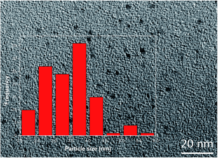 | ||
| Fig. 1 TEM micrograph of the thiol-capped CdTe quantum dots. Inset of the histogram of the particle size of the thiol-capped CdTe quantum dots. | ||
The optical emission and absorption spectra were recorded for the CdTe QDs (Fig. 2).
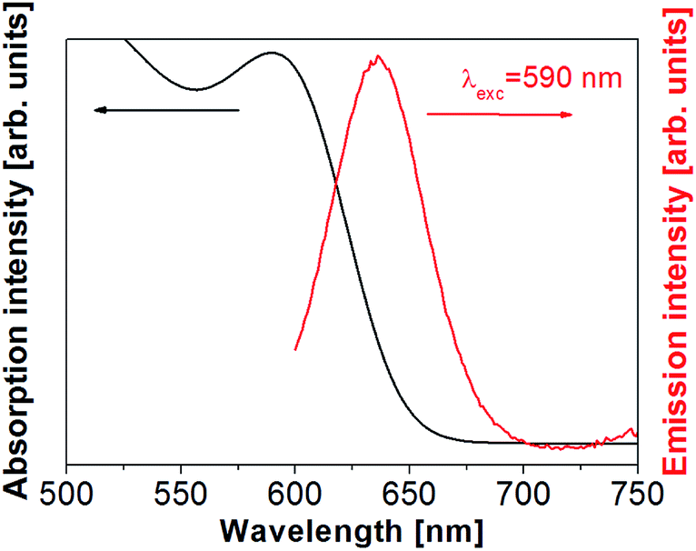 | ||
| Fig. 2 Optical characterization of the thiol-capped CdTe QD. In red, the emission spectrum and in black the absorption spectrum. | ||
The emission band was centered at 634 nm and the absorption maximum lays at 570 nm. These spectra are in good agreement with the known optical features of CdTe QDs.38 Further characterization of the thiol-capped CdTe QDs can be found elsewhere.38
Characterization of CdTe–saponites
The synthesized clay mineral was identified as saponite by XRPD and its delamination was corroborated by the absence of the reflection (001) in the X-ray diffractogram (not shown here). TEM microscopy confirmed the presence of very thin lamellae at monolayer level, with thicknesses between 1.5 and 2.5 nm, randomly oriented and moderately aggregated (Fig. 3). The results were similar to those previously published.35,39 | ||
| Fig. 3 TEM micrograph of the dS sample. | ||
The delaminated saponite (dS) was exchanged with the cationic polyelectrolyte poly(diallyldimethylammonium chloride) (PDDA) and thioglycolic acid capped CdTe QDs (CdTe–dSPDDA). FT-IR analysis was performed in order to detect the presence of the cationic surfactant intercalation and the CdTe QDs (Fig. 4).
 | ||
| Fig. 4 FT-IR spectrum for the CdTe–dSPDDA sample. | ||
In addition to the typical absorption bands of saponite,39 the characteristic absorption bands corresponding to PDDA were also found in the spectrum:40 the CH2 asymmetrical and symmetrical stretching vibrations (2923 and 2853 cm−1) and the CH2 deformation vibration (1466 cm−1). The band at 1637 cm−1, corresponding to C![[double bond, length as m-dash]](https://www.rsc.org/images/entities/char_e001.gif) C stretching vibration, could be also considered a characteristic band of the PDDA40 but in our spectrum the bending mode of adsorbed water on the saponite appeared in the same position, difficulting the assignation of this band. The band at around 1384 cm−1 (Fig. 4) was assigned to the stretching vibration of the COO− group that belongs to the ligands of the thiol-capped CdTe QDs, by comparison with the assignations found in the literature for these nanoparticles.41,42 This was corroborated by the fact that this band was not observed in the spectra of saponite or PDDA.39,40
C stretching vibration, could be also considered a characteristic band of the PDDA40 but in our spectrum the bending mode of adsorbed water on the saponite appeared in the same position, difficulting the assignation of this band. The band at around 1384 cm−1 (Fig. 4) was assigned to the stretching vibration of the COO− group that belongs to the ligands of the thiol-capped CdTe QDs, by comparison with the assignations found in the literature for these nanoparticles.41,42 This was corroborated by the fact that this band was not observed in the spectra of saponite or PDDA.39,40
Characterization of the composites dS/PDDA/CdTe and dSPDDA/CdTe
Two composites were assembled by deposition of films of dS, PDDA and CdTe QDs (dS/PDDA/CdTe) and by deposition of dSPDDA and CdTe QDs (dSPDDA/CdTe).The morphology of the assembled composites on the glass substrates were checked by SEM microscopy. Micrographs of dS/PDDA/CdTe (Fig. 5a) and dSPDDA/CdTe (Fig. 5b) showed the external disposition of the cationic polyelectrolyte in both composites. It was not possible to distinguish the presence of the delaminated clay, which probably was oriented during the spin-coating process and covered by the PDDA. The CdTe QDs were not observed either due to the small size of their particles. However, differences in the morphology of both assembled composites were observed. There is some aggregation of the PDDA in Fig. 5a, probably due to some loss of homogeneity during the spin-coating process. Interestingly, the disposition of the PDDA along the surface for dSPDDA/CdTe composite was more homogeneously distributed. The fissures located in Fig. 5b could be formed as a result of non-uniform evaporation of the solvent containing the dSPDDA solution during the spin coating process.
 | ||
| Fig. 5 (a) SEM micrograph of the dS/PDDA/CdTe sample at 5k, (b) SEM micrograph of the dSPDDA/CdTe sample at 5k. | ||
Luminescence characterization
The emission spectra at room temperature under excitation at 590 nm for CdTe–dSPDDA sample and 580 nm for composite dSPDDA/CdTe and dS/PDDA/CdTe samples are shown in Fig. 6a and b, respectively. | ||
| Fig. 6 Emission spectra of (a) CdTe–dSPDDA sample and (b) dSPDDA/CdTe and dS/PDDA/CdTe samples. | ||
In systems formed by colloidal QDs aggregates, it has been published that the QDs emission exhibited a red-shifting as the presence of aggregate size increased.19 Besides, Liang et al. already reported a slight red shift of the QDs emission when a composite was formed with layered double hydroxide (LDH) nanosheets; in this case, the origin of the shift was related to the electronic effects produced by the electrostatic interactions between the QDs and the LDH film.27 In our samples, a red shift was only observed for the sample CdTe–dSPDDA, attributed to a certain size increase of QDs aggregates during the synthesis time.
The differences within the emission intensities between the two composite samples, dS/PDDA/CdTe and dSPDDA/CdTe could be associated to the quantity of the QDs in the composites after the drop casting process. The larger presence of the cationic polyelectrolyte in terms of surface for sample dS/PDDA/CdTe compared to sample dSPDDA/CdTe could explain this behaviour, meaning more quantity of QDs. Additionally, in the SEM micrograph of dSPDDA/CdTe we can observe a more wrinkled surface compared to that of sample dS/PDDA/CdTe. This could lead also to more scattering areas and subsequently a weaker emitted light.
The clear blue shift in the optical emission observed for the composites dSPDDA/CdTe and dS/PDDA/CdTe could be attributed to the disaggregation of the QDs in these composites, and also some effect of siever by the procedure in which the smallest QDs were more stabilized in the sample.
Electrical characterization of light-emitting diode (LED) ITO/PEDOT:PSS/(dS/PDDA/CdTe)6/Au/Ag
A light-emitting diode (LED) was assembled with an emissive layer based on 6 cycles of alternated depositions by spin-coating of dS, PDDA and dip coating of CdTe QDs films. ITO and Au/Ag were chosen as contact due to their values of work function, being respectively 5.53 eV and around 5.47 eV. The work function of the materials chosen to be a good ohmic contact should be equal or higher to the sum of the electron affinity and energy gap of the material.43 Despite these properties are difficult to know for saponites, for the CdTe this value is 5.73 eV. Therefore, we expected to have an ohmic contact. In addition, ITO was chosen due to its transparency to the visible light.The I–V characteristics at room temperature of the device are shown in Fig. 7. From the slope of the plot logV vs. logI it is possible to obtain information regarding the electronic conduction mechanism in each region of the curve.44
 | ||
| Fig. 7 I–V characteristics for the ITO/PEDOT:PSS/(dS/PDDA/CdTe)6/Au/Ag device at room temperature. | ||
Two differentiated regions can be observed in the curve: a first region between 0 and 5.2 V where the current is directly proportional to the applied voltage, thus indicating ohmic conduction (slope = 1),45 and a second region starting at 5.2 V, which is the turn-on voltage, where starts the nonlinearity in the I–V curve, meaning that the injected charge density exceeds the intrinsic free carrier density of the material.
This region is governed by space charge limited conduction (SCLC) (slope ≈ 2) where photocurrent originates.
The close similarity with the architecture of previously reported QD-based devices15 suggest us that the main conduction mechanism could be governed by charge hopping between the nanocrystals mediated by tunnelling injection through the saponite sheets.
In light of these results, further research would be interesting to complete the characterization of the device and to explore the different applications mentioned in the Introduction section that potentially could use these hybrid materials.
Conclusions
Several composite materials based on delaminated saponites, where thiol-capped CdTe quantum dots were hosted, have been synthesized. For the composite material exchanged with PDDA and thiol-capped QDs CdTe the presence of the QDs was confirmed by FT-IR spectroscopy and by photoluminescence measurements. Two additional composites (dS/PDDA/CdTe and dSPDDA/CdTe) were synthesized by LbL using spin-coating technique in order to obtain an architecture suitable for nanotechnology applications. Photoemission in the red region of the visible spectrum was detected for all the composite materials. In order to test one of the composite assemblies with dS, PDDA and the CdTe QDs, a light-emitting diode was assembled and its electrical I–V characteristics characterized. Photocurrent, originated by the electron–hole tunnelling recombination in the QD emissive layer with a turn-on voltage of 5.2 V, was observed.Acknowledgements
The authors are grateful for the financial support of Ministerio de Economía y Competitividad of Spain, FEDER funds (CTQ2009-12520-C03-02, CTQ-2011-24610, TEC2015-71324-R (MINECO/FEDER), MAT2013-47395-C4-4-R), ICREA under the ICREA Academia Award, Catalan authority under projects (2014SGR1344, 2014SGR1146 and 2014SGR1358) and from Universitat Rovira i Virgili scholarship program for PhD grant.References
- J. Y. Kim, O. Voznyy, D. Zhitomirsky and E. H. Sargent, Adv. Mater., 2013, 25, 4986 CrossRef CAS PubMed.
- Y. Zhang, Y. Chen, P. Westerhoff and J. C. Crittenden, Environ. Sci. Technol., 2008, 42, 321 CrossRef CAS PubMed.
- H. M. E. Azzazy, M. M. H. Mansour and S. C. Kazmierczak, Clin. Biochem., 2007, 40, 917 CrossRef CAS PubMed.
- Y. Wang and L. Chen, Nanomedicine, 2011, 7, 385 CAS.
- V. Biju, Chem. Soc. Rev., 2014, 43, 744 RSC.
- A. J. Shuhendler, P. Prasad, H.-K. C. Chan, C. R. Gordijo, B. Soroushian, M. Kolios, K. Yu, P. J. O'Brien, A. M. Rauth and X. Y. Wu, ACS Nano, 2011, 5, 1958 CrossRef CAS PubMed.
- M. Lu, W. Zhang, Y. Gai, T. Yang, P. Ye, G. Yang, X. Ma and G. Xiang, New J. Chem., 2014, 38, 4519 RSC.
- W.-Y. Rho, J.-W. Choi, H.-Y. Lee, S. Kyeong, S. H. Lee, H. S. Jung, S. Jung, Y.-E. Sung, Y.-S. Lee and B.-H. Jun, New J. Chem., 2014, 38, 910 RSC.
- H. Cao, Z. Liu, X. Zhu, J. Peng, L. Hu, S. Xu, M. Luo, W. Ma, J. Tang and H. Liu, Nanotechnology, 2015, 26, 035401 CrossRef CAS PubMed.
- V. M. Blas-Fernando, J. Ortiz, V. González-Pedro, R. S. Sánchez, I. Mora-Seró, F. Fernández-Lázaro and A. Sastre-Santos, Chem. Commun., 2015, 51, 1732 RSC.
- N.-Y. Kim, S.-H. Hong, J.-W. Kang, N. Myoung, S.-Y. Yim, S. Jung, K. Lee, C. W. Tu and S.-J. Park, RSC Adv., 2015, 5, 19624 RSC.
- D. Costenaro, F. Carniato, G. Gatti, L. Marchese and C. Bisio, New J. Chem., 2014, 38, 6205 RSC.
- R. Liang, D. Yan, R. Tian, X. Yu, W. Shi, C. Li, M. Wei, D. G. Evans and X. Duan, Chem. Mater., 2014, 26, 2595 CrossRef CAS.
- J. Zhang, F.-X. Xiao, G. Xiao and B. Liu, New J. Chem., 2015, 39, 279 RSC.
- J. S. Bendall, M. Paderi, F. Ghigliotti, N. L. Pira, V. Lambertini, V. Lesnyak, N. Gaponik, G. Visimberga, A. Eychmüller, C. M. Sotomayor Torres, M. E. Welland, C. Gieck and L. Marchese, Adv. Funct. Mater., 2010, 20, 3298 CrossRef CAS.
- Y. Zhou, D. Yan and M. Wei, J. Mater. Chem. C, 2015, 3, 10099 RSC.
- F.-X. Xiao, J. Miao and B. Liu, J. Am. Chem. Soc., 2014, 136, 1559 CrossRef CAS PubMed.
- M. Müller, M. Kaiser, G. M. Stachowski, U. Resch-Genger, N. Gaponik and A. Eychmüller, Chem. Mater., 2014, 26, 3231 CrossRef.
- Y.-C. Cao, J. Colloid Interface Sci., 2012, 368, 139 CrossRef CAS PubMed.
- N. Khaorapapong, A. Ontam and M. Ogawa, Appl. Clay Sci., 2010, 50, 19 CrossRef CAS.
- H. Li, J. Liu, K. Wang, X. Yu, S. Zuo and B. Li, Mater. Lett., 2013, 107, 284 CrossRef CAS.
- A. Ontam, N. Khaorapapong and M. Ogawa, J. Mater. Chem., 2012, 22, 20001 RSC.
- H.-Y. Xie, J. Yang, S.-Y. Yang, C.-F. Wang, L. Chen and S. Chen, Mater. Lett., 2011, 65, 1669 CrossRef CAS.
- M. Algarra, A. Reis, I. Bobos, B. B. Campos, J. Jiménez-Jiménez, R. Moreno-Tost and J. C. G Esteves da Silva, J. Dispersion Sci. Technol., 2012, 33, 1139 CrossRef CAS.
- J. T. Kloprogge, S. Komarneni and J. E. Amonette, Clays Clay Miner., 1999, 47, 529 CAS.
- C. Bisio, G. Gatti, E. Boccaleri, L. Marchese, G. B. Superti, H. O. Pastore and M. Thommes, Microporous Mesoporous Mater., 2008, 107, 90 CrossRef CAS.
- R. Liang, R. Tian, W. Shi, Z. Liu, D. Yan, M. Wei, D. G. Evans and X. Duan, Chem. Commun., 2013, 49, 969 RSC.
- W. Zhou, W. Guan and C. Lu, Chem. Commun., 2014, 50, 11370 RSC.
- X. Xu, F. Zhang, S. Xu, J. He, L. Wang, D. G. Evans and X. Duan, Chem. Commun., 2009, 7533 RSC.
- C.-H. Zhou, Z.-F. Shen, L.-H. Liu and S.-M. Liu, J. Mater. Chem., 2011, 21, 15132 RSC.
- S. Srivastava and N. A. Kotov, Acc. Chem. Res., 2008, 41, 1831 CrossRef CAS PubMed.
- M. Gao, C. Lesser, S. Kirstein, H. Möhwald, A. L. Rogach and H. Weller, J. Appl. Phys., 2000, 87, 2297 CrossRef CAS.
- Y.-W. Lin, W.-L. Tseng and H.-T. Chang, Adv. Mater., 2006, 18, 1381 CrossRef CAS.
- Z. Li, S. Wan, W. Xu, Y. Wang, B. R. Shah, W. Jin, Y. Chen and B. Li, J. Appl. Polym. Sci., 2015, 132, 41893 Search PubMed.
- F. B. Gebretsadik, P. Salagre and Y. Cesteros, Appl. Clay Sci., 2014, 87, 170 CrossRef CAS.
- H. Hata, S. Kubo, Y. Kobayashi and T. E. Mallouk, J. Am. Chem. Soc., 2007, 129, 3064 CrossRef CAS PubMed.
- C. de Mello Donegá and R. Koole, J. Phys. Chem. C, 2009, 113, 6511 Search PubMed.
- N. Gaponik, D. V. Talapin, A. L. Rogach, K. Hoppe, E. V. Shevchenko, A. Kornowski, A. Eychmüller and H. Weller, J. Phys. Chem. B, 2002, 106, 7177 CrossRef CAS.
- R. Trujillano, E. Rico, M. A. Vicente, V. Rives, K. J. Ciuffi, A. Cestari, A. Gil and S. A. Korili, Appl. Clay Sci., 2011, 53, 326 CrossRef CAS.
- D.-Q. Yang, J.-F. Rochette and E. Sacher, J. Phys. Chem. B, 2005, 109, 4481 CrossRef CAS PubMed.
- M. S. Abd El-sadek and S. Moorthy Babu, Phys. B, 2010, 405, 3279 CrossRef CAS.
- F. O. Silva, M. S. Carvalho, R. Mendonça, W. A. A. Macedo, K. Balzuweit, P. Reiss and M. A. Schiavon, Nanoscale Res. Lett., 2012, 7, 536 CrossRef PubMed.
- Principles of Semiconductor Devices, http://ecee.colorado.edu/%7Ebart/book/book/title.htm, accessed October 2016.
- S. M. Sze and K. K. Ng, Physics of semiconductor devices, Wiley, New York, 3rd edn, 2007 Search PubMed.
- D. Joung, A. Chunder, L. Zhai and S. I. Khondaker, Appl. Phys. Lett., 2010, 97, 093105 CrossRef.
Footnotes |
| † Present address: School of Physical and Geographical Sciences, Keele University, Staffordshire, ST5 5BG, UK. |
| ‡ Present address: School of Chemistry, Newcastle University, Newcastle upon Tyne, NE1 7RU, UK. |
| This journal is © The Royal Society of Chemistry 2016 |