
Outstanding electromagnetic interference shielding effectiveness of polyvinylbutyral–polyaniline nanocomposite film
Pritom J. Boraa,
Gaurav Lakhanib,
Praveen C. Ramamurthy*ab and
Giridhar Madras a
a
aInterdisciplinary Centre for Energy Research (ICER), Indian Institute of Science (IISc), Bangalore-560012, India. E-mail: onegroupb203@gmail.com
bDepartment of Materials Engineering, Indian Institute of Science (IISc), Bangalore-560012, India
First published on 8th August 2016
Abstract
In this study, we studied the electromagnetic interference (EMI) shielding property of a solution processed polyvinylbutyral–polyaniline nanocomposite (PVBPN) film in the X-band (8.2–12.4 GHz) and Ku-band (12.4–18 GHz) frequency. The polyaniline nanofibers were chemically synthesized at −30 ± 2 °C and characterized by various techniques. The optimally prepared, free standing PVBPN film (sandwiched 0.78 ± 0.02 mm) shows an outstanding EMI shielding effectiveness in the X-band and Ku-band frequency. In the X-band, ∼26 dB EMI shielding effectiveness (shielding due to absorption SEA ∼ 21 dB and shielding due to reflection SER ∼ 5 dB) was obtained and was found to increase ∼30 dB (SEA is ∼26 dB and SER ∼ 4 dB) for the Ku-band. The enhancement of shield conductivity, dielectric loss and EM attenuation constant with frequency results in the excellent EMI shielding property of the PVBPN film.
1. Introduction
At present, due to the prospective applications of electrical/electronics, electromagnetic interference (EMI) shielding materials are in demand, especially for the high frequency range (8.2–18 GHz).1–5 The electromagnetic interference shielding by a material for an incident plane wave, i.e. radiated electromagnetic wave in the far field of the source, is equal to the EMI attenuation due to absorption, reflection and multiple reflections (correction factor/scattering loss).3–5 Thus, the total EMI shielding effectiveness is expressed as,| SET = SEA + SER + SEM |
Lightweight, flexible polymer nanocomposite materials have been a key interest for EMI shielding and microwave absorption because of their many advantages over traditionally used metal sheets.3–8 Intrinsic conducting polymers (ICPs) such as polyacetylene (PA), polypyrol (PPY), polyaniline (PANI) are well known for EMI shielding.9 Among them, PANI has drawn special attention because of its bulk level easy synthesis, tunable conductivity and molecular weight.9–12 The electrical conductivity of PANI depends on its molecular weight and synthesizing temperature. A low temperature synthesis (∼−30 °C) has been proposed for high molecular weight PANI with higher conductivity.12 However, the electrical conductivity of polyaniline decreases over time because of de-doping.10 It has been shown that PANI in a non-conducting polymer matrix shows better stability with EMI shielding.13–15 Lakshmi et al. reported the EMI shielding behaviour of PU–PANI composite in the S-band and X-band frequencies.13 According to their results, 1.9 mm thick PU–PANI (PU![[thin space (1/6-em)]](https://www.rsc.org/images/entities/char_2009.gif) :aniline ratio was 1:1) composite shows a maximum ∼26.7 dB shielding effectiveness at 8.8 GHz. However, the average SE is ∼10 dB in the frequency range 8–12 GHz.13 Similarly, Sudha et al. reported 16.2 dB SE with 10 weight% PANI clay loaded polystyrene (PS) composite (1 mm thickness) at a frequency of 8 GHz.14 Saini et al. studied the EMI shielding behaviour of PANI–multiwall CNT–PS nanocomposite.15 Their study shows ∼24 dB SE of 30 weight% PANI–multiwall CNT loaded PS nanocomposite (thickness 1 mm) in the frequency range of 12.4–18 GHz. When the thickness was increased to 2 mm, the SET value reached 40–45 dB.15
:aniline ratio was 1:1) composite shows a maximum ∼26.7 dB shielding effectiveness at 8.8 GHz. However, the average SE is ∼10 dB in the frequency range 8–12 GHz.13 Similarly, Sudha et al. reported 16.2 dB SE with 10 weight% PANI clay loaded polystyrene (PS) composite (1 mm thickness) at a frequency of 8 GHz.14 Saini et al. studied the EMI shielding behaviour of PANI–multiwall CNT–PS nanocomposite.15 Their study shows ∼24 dB SE of 30 weight% PANI–multiwall CNT loaded PS nanocomposite (thickness 1 mm) in the frequency range of 12.4–18 GHz. When the thickness was increased to 2 mm, the SET value reached 40–45 dB.15
Anisotropic nanoparticles, especially groups of nanofibers or nanotree structures with high dielectric loss, are reported as better microwave absorbers compared to other nanostructures.16 Mechanistically, they act like a receiver antenna that transforms electromagnetic radiation (EM energy) to a microcurrent that propagates through the material.16 Hence, it loses energy through dissipation of the current and shows high microwave absorption. Recent investigations show PANI nanofibers exhibit some interesting behaviours, and they have been proposed for many potential applications including biocompatibility,17 sensors,18 EMI shielding19 as well as for heat conduction.20
Polyvinylbutyral (PVB), a novel polymer, has recently drawn much attention for encapsulation, especially in organic electronics, because of its unique moisture resistive and dielectric properties.21,22 Hence, a PVB–PANI nanofiber composite film can be expected as a potential polymer nanocomposite to coat small modern communication devices to protect against EMI. To the best of our knowledge, the EMI shielding property of the PVB–PANI nanofiber composite film is not reported. The objective of the present work is the synthesis of PANI nanofibers at low temperature, preparation of PVB–PANI nanofiber composite films and investigation of the EMI shielding property.
2. Experimental
2.1. Synthesis and film preparation
The PANI nanofibers were synthesized by oxidative polymerization of aniline (double distilled) at −30 ± 2 °C in an acidic aqueous(HCl)–organic(chloroform) two phase system, according to the procedure described in the literature.23 The commercially available PVB (4 g) was dissolved in 30 ml ethanol and optimally 1.15 g of as synthesized PANI nanofibers were added slowly to the PVB solution and stirred for another 2 h. The solution was then poured into a polyethylene terephthalate (PET) mould and kept for air drying (12 h). The obtained PVB–PANI nanocomposite film was named as the PVBPN film. Three films were sandwiched for EMI shielding measurements, and the thickness was found to be 0.78 ± 0.02 mm.2.2. Characterization and EMI shielding measurement
The surface morphologies of the synthesized PANI nanofibers were analysed using high resolution FESEM (Carl Zeiss). The UV-visible spectra of the polyaniline nanofiber were obtained by a Perkin spectrophotometer. The X-ray diffractogram was obtained through a Rigaku X-ray diffractometer using Cu Kα radiation (λ = 1.540598 Å) in a scattering range (2θ) of 10–80°. The EMI shielding effectiveness was measured by using a vector network analyser (VNA, Agilent NS201). The scattering parameters (S-parameters, S21 and S11) were determined by waveguide method after performing standard thru–reflect–line (TRL) calibration of VNA for the X-band (8.2–12.4 GHz) and Ku-band (12.4–18 GHz). The complex S-parameters (S21 and S11) of the three sample films were measured for each frequency band. The EMI shielding effectiveness in dB is equal to |S21|.24 The reflectance (R), absorbance (A) and transmittance (T) were obtained from the measured S-parameters, and EMI shielding due to absorption (SEA) and reflection (SER) was investigated. The mathematical interpretations of SEA, SER and SEM are15
| SER (dB) = −10log(1 − R) |
| SEM (dB) = −20log(1 − 10−SEA/10) |
The real and imaginary part of the complex permittivity (ε* = ε′ − iε′′) was determined from the obtained S-parameters by using the standard Nicholsion–Ross–Weir (NRW) method.25
3. Results and discussion
The surface morphology of the as synthesized PANI nanofibers is shown in Fig. 1(a) and (b). The diameters of the PANI fibres were found to be 70–90 nm whilst the length was ∼1 μm. Moreover, a few small agglomerated regions were also observed. The UV-visible spectrum of the as synthesized PANI nanofibers in N-methyl-2-pyrrolidone (NMP) is shown in Fig. 1(c). The two strong absorption bands obtained at 326 nm and 633 nm correspond to the π–π* transition and quinoid ring transition, respectively, in the polyaniline chain and implies an interaction between the PANI nanofiber and NMP.26,27 Since NMP is a highly polar solvent, in the presence of the PANI nanofiber, the solute–solvent interactions become strong. According to the literature,27 it results in a de-protonation of the polyaniline chain (through hydrogen bonding) and conversion of the emaraldine salt (ES) to an emaraldine base (EB).27 The X-ray diffraction pattern of PANI nanofiber is shown in Fig. 1(d). The obtained diffractogram suggests the semi crystalline nature of as synthesized PANI nanofibers.28 The appearance of three peaks in the diffractogram at 2θ values of 15°, 20° and 25° suggest the formation of a conducting PANI nanofiber.27,28 | ||
| Fig. 1 (a and b) Surface morphology, (c) UV-visible spectrum and (d) X-ray diffraction pattern of synthesized PANI nanofibers. | ||
The FTIR spectrum of synthesized PANI nanofibers is shown in Fig. 2. As shown in Fig. 2, the observed peaks at ∼1591 cm−1 and at ∼1495 cm−1 represent C![[double bond, length as m-dash]](https://www.rsc.org/images/entities/char_e001.gif) C stretching vibrations of the quinoid and benzoid rings, respectively.12 1400–1000 cm−1 is the C–N stretching region for secondary aromatic amines. The most prominent peak is at 1319, representing the C–N stretching for aromatic amines. In the finger print region, the prominent peak at 829 cm−1 is thought to arise from C–H out of plane bending modes.12
C stretching vibrations of the quinoid and benzoid rings, respectively.12 1400–1000 cm−1 is the C–N stretching region for secondary aromatic amines. The most prominent peak is at 1319, representing the C–N stretching for aromatic amines. In the finger print region, the prominent peak at 829 cm−1 is thought to arise from C–H out of plane bending modes.12
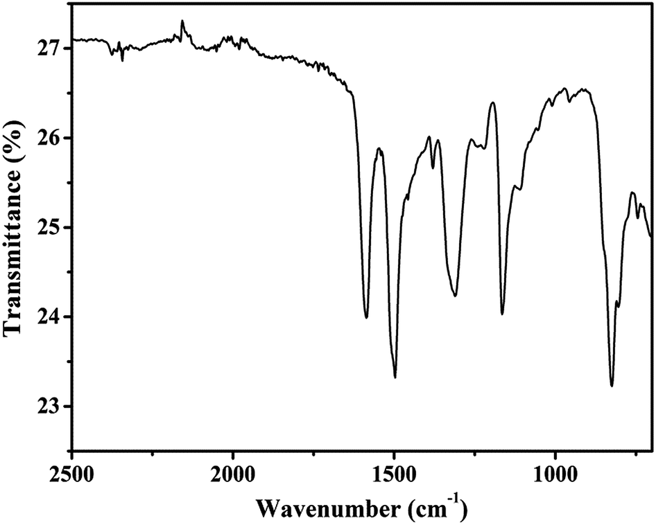 | ||
| Fig. 2 FTIR spectrum of synthesized PANI nanofibers. | ||
The cross sectional surface morphology, FTIR spectrum and XRD pattern of a prepared PVBPN nanocomposite film are shown in Fig. 3 along with its optical images. The cross sectional SEM images of the PVBPN film (Fig. 3(b) and (c)) show the distribution of the PANI nanofibers in the PVBPN film. It suggests an improvement in the loss factor and dielectric loss can take place along the PANI nanofibers that can enhance EMI SE through absorption. In the FTIR spectrum of the PVBPN film (Fig. 3(e)), the broad peak at ∼3296 cm−1 is assigned to the OH stretching of the alcohol fragment of PVB. The peaks at ∼2918 and 2870 correspond to the asymmetric and symmetric CH2 stretching, whereas the peak at ∼1432 cm−1 is believed to be due to the CH2 bending.21 The peak observed at 1732 cm−1 suggests carbonyl stretching of the acetate fragment of the PVB.21 Fig. 3(f) shows the XRD pattern of the PVBPN nanocomposite film, and the wide diffraction peak of PVB (2θ = 20°) was observed with the most prominent PANI nanofiber peak (2θ = 25°). Thus, it suggests the presence of PANI nanofibers in the PVBPN film.
 | ||
| Fig. 3 (a and b) Optical images, (c and d) cross-sectional SEM images, (e) FTIR spectrum and (f) XRD pattern of PVBPN film. | ||
The variation of the obtained total EMI shielding effectiveness (SET), shielding effectiveness due to absorption (SEA) and shielding effectiveness due to reflection (SER) of the PVBPN nanocomposites in the X-band (8.2–12.4 GHz) and Ku-band (12.4–18 GHz) frequency range are shown in Fig. 4(a) and (b), respectively. In the X-band, the average SET value was obtained at ∼26 dB (SEA is ∼21 dB and SER is ∼5 dB) and was found to increase to ∼30 dB (SEA is ∼26 dB and SER is ∼4 dB) in the Ku-band. Thus, it was observed that the EMI SE of PVBPN increased with frequency (8.2–18 GHz), and the EMI shielding due to absorption of the nanocomposite is much higher than EMI shielding due to reflection. The average specific EMI SE of the PVBPN film in the X-band was ∼72 ± 2 dB cm3 g−1 while in Ku-band it was ∼91 ± 2 dB cm3 g−1. A comparison of the EMI shielding property of as prepared sandwiched PVBPN nanocomposite film with recently developed PANI composites under optimized conditions is tabulated in Table 1.
 | ||
| Fig. 4 Variation of the total EMI shielding effectiveness (SET), shielding due to absorption (SEA) and shielding due to reflection (SER) of PVBPN film in the (a) X-band (8.2–12.4 GHz) and (b) Ku-band (12.4–18 GHz). | ||
| Material | Frequency | SET (dB) | SEA (dB) | SER (dB) | Thickness | Reference |
|---|---|---|---|---|---|---|
| Fe3O4@PANI/polyazomethine/polyetheretherketone | 2–18 GHz | ∼10 | ∼8 | ∼2 | 2 mm | 29 |
| SBS–PANI·DBSA | 7.8–12.4 GHz | ∼35 | — | — | 2 mm | 30 |
| PANI–CNT/polystyrene | 12.4–18 GHz | ∼24 | ∼18 | ∼6 | 1 mm | 15 |
| Polystyrene–PANI–clay | 8 GHz | 16.2 | — | — | 1 mm | 14 |
| PU–PANI | 8–12 GHz | ∼10 | — | — | 1.9 mm | 13 |
| PVB–PANI nanofiber | 8.2–12.4 GHz | ∼26 | ∼21 | ∼5 | 0.78 ± 0.02 mm | Present work |
| 12.4–18 GHz | ∼30 | ∼26 | ∼4 | Present work |
The incident electromagnetic wave generates an electric field over the conducting PVBPN surface opposite the applied field as the electron cloud near the surface gets distorted, and it passes through the PVBPN nanocomposite by changing its time average power,  .31 Due to this, the incident electromagnetic wave phases change and the magnitude decreases exponentially.31 The real part of the propagation constant,
  , (ω is the angular frequency, ω = 2πf, μ′ is the permeability and σs is the shield conductivity, σs = ωε0ε′′) determines the EMI attenuation due to absorption (EM attenuation constant, α).7
The distance required for the electromagnetic wave to be attenuated to 1/e of its initial amplitude is known as the skin depth or penetration depth (δs),3,7 mathematically,  . For electrically thick shielding materials,7,31,32


The variation of real and imaginary parts of the complex permittivity (ε* = ε′ − iε′′) of the PVBPN film in the X-band is shown in Fig. 5(a) along with the dielectric loss tangent (tanδ = ε′′/ε′, Fig. 5(b)), shield conductivity (Fig. 5(c)) and EM attenuation constant (Fig. 5(d)). The real part of the complex permittivity (ε′) corresponds to the amount of polarization that occurred inside the shield material and the imaginary part (ε′′) corresponds to the dissipation of electrical energy.7,32 It was observed that both ε′ and ε′′ decrease with frequency due to the decrease of the interfacial polarization and heterogeneity of PVB and PANI nanofiberes.3,7 The shield conductivity of the PVBPN film was 49–58 S m−1 and the EM attenuation constant was 950–1170. In the case of the Ku-band, the shield conductivity increased to 67–87 S m−1 (Fig. 6(c)) with high dielectric loss tangent (Fig. 6(b)). The enhancement of conductivity of the PVBPN film with frequency is due to the increased order and compactness of the PANI nanofibers in the PVB matrix. The variation of the EM attenuation constant of PVBPN film in the Ku-band is shown in Fig. 6(d). Compared to the X-band, the EM attenuation constant of the PVBPN film in the Ku-band is high (1500–1980). Thus, it suggests the excellent EMI shielding due to the absorption property of the PVBPN film with frequency. The calculated penetration depth (δs) of the PVBPN film in the X-band and Ku-band is shown in Fig. 7(a) and (b), respectively. As shown in Fig. 7(a), the penetration depth of the PVBPN film exponentially decreases from ∼0.77 mm to ∼0.61 mm in the X-band. Similarly, in the Ku-band, it decreases from ∼0.53 mm to ∼0.4 mm. Thus, the decrease in the penetration depth of the PVBPN film with frequency also results in an enhancement of the EMI shielding due to absorption. Each PANI nanofiber in the composite is surrounded by the effective medium. Hence, the attenuation of the incident electromagnetic radiation also takes place due to the scattering.
 | ||
| Fig. 5 Variation of (a) real and imaginary parts of the complex permittivity, (b) dielectric loss, (c) shield conductivity and (d) EM attenuation constant of the PVBPN film in the X-band. | ||
 | ||
| Fig. 6 Variation of (a) real and imaginary parts of the complex permittivity, (b) dielectric loss, (c) shield conductivity and (d) EM attenuation constant of the PVBPN film in the Ku-band. | ||
 | ||
| Fig. 7 Variation of the penetration depth of the PVBPN film in the (a) X-band and (b) Ku-band frequency. | ||
The scattering attenuation depends on the number of particles (nanofibers) in a volume in the effective medium.33 The equation of scattering attenuation (Isc) is33,34

4. Conclusion
The PANI nanofibers were successfully synthesized at −30 ± 2 °C. Investigation of the EMI shielding property of the optimally prepared PVB–polyaniline nanofiber composite (PVBPN) flexible film shows an outstanding EMI shielding effectiveness for the X-band and Ku-band frequency range with an appreciable film thickness. The 0.78 ± 0.02 mm thicker sandwiched PVBPN film shows ∼26 dB and ∼30 dB EMI shielding effectiveness for the X-band and Ku-band, respectively. Mechanistically, EMI shielding due to absorption was found to be dominant for each band. Furthermore, enhancement of conductivity, dielectric loss and the EM attenuation constant with frequency show excellent EMI shielding due to absorption of the PVBPN film.Acknowledgements
Authors gratefully acknowledge the prof. K. J. Vinoy, Dept. of Electrical and Communication Engineering, IISc, India for his help during the EMI shielding, dielectric measurements and some valuable discussions. This work is financially supported by Department of Science and Technology SB/S3/ME/51/2012 and technically supported by IISc advanced characterization centre and CeNSE.References
- M. H. Al-Saleh, W. H. Saadeh and U. Sundararaj, Carbon, 2013, 60, 146–156 CrossRef CAS.
- J. Li, G. Zhang, Z. Ma, X. Fan, X. Fan, J. Qin and X. Shi, Compos. Sci. Technol., 2016, 129, 70–78 CrossRef CAS.
- X. C. Tong, Advanced Materials and Design for Electromagnetic Interference Shielding, CRC Press, 2008 Search PubMed.
- M. Arjmand, A. A. Moud, Y. Li and U. Sundararaj, RSC Adv., 2015, 5, 56590–56598 RSC.
- Y. Zhang, Z. Wang, B. Zhang, G.-L. Zhao and S. M. Guo, RSC Adv., 2015, 5, 93499–93506 RSC.
- M. H. Al-Saleh and U. Sundararaj, Carbon, 2009, 47, 1738–1746 CrossRef CAS.
- J. W. Gooch and J. K. Daher, Electromagnetic Shielding and Corrosion Protection for Aerospace Vehicles, Springer New York, New York, NY, 2007 Search PubMed.
- Z. Chen, C. Xu, C. Ma, W. Ren and H.-M. Cheng, Adv. Mater., 2013, 25, 1296–1300 CrossRef CAS PubMed.
- J. Joo and A. J. Epstein, Appl. Phys. Lett., 1994, 65, 2278–2280 CrossRef CAS.
- H. S. Nalwa, Handbook of Organic Conductive Molecules and Polymers, Charge-Transfer Salts, Fullerenes and Photoconductors, Wiley, 1997 Search PubMed.
- P. Saini, V. Choudhary, N. Vijayan and R. K. Kotnala, J. Phys. Chem. C, 2012, 116, 13403–13412 CAS.
- P. C. Ramamurthy, A. N. Mallya, A. Joseph, W. R. Harrell and R. V. Gregory, Polym. Eng. Sci., 2012, 52, 1821–1830 CAS.
- K. Lakshmi, H. John, K. T. Mathew, R. Joseph and K. E. George, Acta Mater., 2009, 57, 371–375 CrossRef CAS.
- J. D. Sudha, S. Sivakala, K. Patel and P. Radhakrishnan Nair, Composites, Part A, 2010, 41, 1647–1652 CrossRef.
- P. Saini, V. Choudhary, B. P. Singh, R. B. Mathur and S. K. Dhawan, Synth. Met., 2011, 161, 1522–1526 CrossRef CAS.
- R. F. Zhuo, L. Qiao, H. T. Feng, J. T. Chen, D. Yan, Z. G. Wu and P. X. Yan, J. Appl. Phys., 2008, 104, 94101 CrossRef.
- A. Kumar, S. Banerjee, J. P. Saikia and B. K. Konwar, Nanotechnology, 2010, 21, 175102 CrossRef CAS PubMed.
- J. Huang, S. Virji, B. H. Weiller and R. B. Kaner, J. Am. Chem. Soc., 2003, 125, 314–315 CrossRef CAS PubMed.
- N. Joseph, J. Varghese and M. T. Sebastian, RSC Adv., 2015, 5, 20459–20466 RSC.
- C. Nath, A. Kumar, K.-Z. Syu and Y.-K. Kuo, Appl. Phys. Lett., 2013, 103, 121905 CrossRef.
- A. S. Roy, S. Gupta, S. Seethamraju, G. Madras and P. C. Ramamurthy, Composites, Part B, 2014, 58, 134–139 CrossRef CAS.
- S. Gupta, S. Seethamraju, P. C. Ramamurthy and G. Madras, Ind. Eng. Chem. Res., 2013, 52, 4383–4394 CrossRef CAS.
- J. Huang and R. B. Kaner, J. Am. Chem. Soc., 2004, 126, 851–855 CrossRef CAS PubMed.
- Y. Yang, M. C. Gupta, K. L. Dudley and R. W. Lawrence, Nano Lett., 2005, 5, 2131–2134 CrossRef CAS PubMed.
- L. F. Chen, C. K. Ong, C. P. Neo, V. V. Varadan and V. K. Varadan, Microwave Electronics: Measurement and Materials Characterization, John Wiley & Sons, 2004 Search PubMed.
- J. G. Masters, Y. Sun, A. G. MacDiarmid and A. J. Epstein, Synth. Met., 1991, 41, 715–718 CrossRef CAS.
- A. Rahy and D. J. Yang, Mater. Lett., 2008, 62, 4311–4314 CrossRef CAS.
- K. Lee, S. Cho, S. Heum Park, A. J. Heeger, C.-W. Lee and S.-H. Lee, Nature, 2006, 441, 65–68 CrossRef CAS PubMed.
- W. Wei, X. Yue, Y. Zhou, Y. Wang, Z. Chen, M. Zhu, J. Fang and Z. Jiang, RSC Adv., 2014, 4, 11159–11167 RSC.
- M. Magioli, B. G. Soares, A. S. Sirqueira, M. Rahaman and D. Khastgir, J. Appl. Polym. Sci., 2012, 125, 1476–1485 CrossRef CAS.
- C. A. Grimes and D. M. Grimes, in, 1993 IEEE Aerospace Applications Conference Digest, 1993, pp. 217–226 Search PubMed.
- Y. Zhang, Z. Wang, B. Zhang, C. Zhou, G.-L. Zhao, J. Jiang and S. M. Guo, J. Mater. Chem. C, 2015, 3, 9684–9694 RSC.
- C. F. Bohren and D. R. Huffman, Absorption and Scattering of Light by Small Particles, John Wiley & Sons, 2008 Search PubMed.
- H. Guan, J. Xie, G. Chen and Y. Wang, Mater. Chem. Phys., 2014, 143, 1061–1068 CrossRef CAS.
| This journal is © The Royal Society of Chemistry 2016 |