DOI:
10.1039/C6RA05765A
(Paper)
RSC Adv., 2016,
6, 58046-58054
A large-volume manufacturing of multi-crystalline silicon solar cells with 18.8% efficiency incorporating practical advanced technologies†
Received
4th March 2016
, Accepted 10th June 2016
First published on 13th June 2016
Abstract
The optimization processes for the mass-production of high-efficiency multi-crystalline silicon solar cells have been observed in this paper. After incorporating several practical advanced technologies such as grain-size controlled low defect-density mc-Si casting ingot, precisely aligned selective emitter, surface-damage free reactive ion etch texturing on a mass production line, the total-area efficiencies up to 18.84% and a production average efficiency of 18.65% for large size (156 × 156 mm2) multi-crystalline silicon (mc-Si) solar cells have been demonstrated, equating to an absolute efficiency gain of 1.58% compared to a conventional solar cell. The corresponding module power is 270.3 W, a 20 W increase over a conventional 60-cell mc-Si module of the same dimensions. These results demonstrate a successful transfer of advanced techniques from laboratory to large scale industrial production, which promote the mc-Si solar cells taking a big step forward in solar cells applications.
1. Introduction
Silicon is the second most abundant element (about 28.2% by weight) in the earth crust and also without contest the most extensively studied element in the periodic table. Crystalline silicon technology represents more than 90% of the entire global photovoltaic (PV) market, of which about 2/3 is taken by mc-Si PV modules. Over the years, the market share of crystalline silicon technologies, and in particular multi-crystalline silicon technology, have fluctuated but have kept at a dominating position which will continue for any foreseeable future. Crystalline silicon PV technology benefits from a well-established silicon-based integrated circuit (IC) industry with its supply chain and manufacturing tools, but its dominance in the global PV market results from a tremendous standardization in technology, materials and manufacturing tools, and a faster learning rate than the other competing PV technologies.1,2 Dramatic improvements in the efficiency of laboratory-scale mc-Si solar cells, from 18% to 20.4% have recently been published.3–5 Nevertheless, these laboratory cells are usually of small dimensions (1–4 cm2) and make use of expensive process steps such as photolithography. Qiao et al.6 reported an 18.5% efficient mc-Si 156 × 156 mm2 solar cell after process optimization of rear AlOx/SiNy stacks deposition and laser structuring. The world record to date for the efficiency of mc-Si solar cells is 20.76% for a 156 × 156 mm2 solar cell fabricated with an industrial “passivated emitter and rear contact” (PERC) process.7 However, the average efficiency of standard full aluminum back surface field (Al-BSF) mc-Si solar cells in mass production usually falls in the range from 17% to 17.5%.
Many studies have been carried out in laboratory in order to improve the mc-Si cell performance, for example, the improvement in wafer quality, the minimization of the front surface reflection losses,8 the development of low-cost selective emitter (SE) processes. Above all, optimizing the mc-Si ingot growth by controlling the grain size with an optimal thermal field and process has proved to be one of the most effective methods to obtain the high-quality mc-Si wafers for low density of dislocations and high carrier lifetime.9–13 The implementation of a SE structure allows the sheet resistance to be reduced to 30–50 Ω □−1 underneath the front metallization to lower the contact resistance and reduce the recombination of minority carriers at the contact.14–16 The SiNx-passivated emitter area in the non-metallized regions has a sheet resistance of 100–120 Ω □−1, resulting in a significant improvement in internal quantum efficiency (IQE) by an average 10–30% absolute in the 300–400 nm wavelength range, and a higher open-circuit voltage (Voc).17,18 Reduction in front surface reflection and enhanced light trapping for mc-Si wafers can be achieved via plasma texturing technology such as reactive ion etching (RIE)19,20 and nano-scale texturing of mc-Si surface using silver assisted wet chemical etching.21 Regardless of grain sizes and orientation, RIE and metal assisted wet chemical etching texturing can reach a reflectance of 1–4% on mc-Si wafers after texturing process.22
Most of the above mentioned technologies are still in laboratory research and few results have been reported on commercial large-size wafers in mass production line, which is attributed to the difficulty of the grain-size control in the ingot growth process, the repeatability of the sheet resistance by the SE process and the surface damage caused by the RIE process.23 These methods were studied in previous publications. Here, the objective of this paper is to present the result of integration of all these process improvements in a large-volume production line (typ. 100 MWp p.a.), resulting in high-efficiency mc-Si cells with a commercial large size of 156 × 156 mm2 fabricated with a simple low-cost process including an advanced ingot growing process, SE structure formation and RIE texturing technologies. An average efficiency of 18.65% was demonstrated over a large production batch, which is the highest value reported so far for large scale industrial production for Al-BSF standard mc-Si solar cells. This result successfully bridges the efficiency gap between the laboratory and the mass production line. Although there are some investments for the newly added equipments, it is very prospective to put these practical advanced technologies into mass production considering the total PV industrial value chain, since the installation unit cost of PV energy system can be reduced 5% by improving 1% absolute conversion efficiency.
2. Power loss analysis of conventional mc-Si solar cells
The saturation current density (J0), which can be written as eqn (1), reflects the recombination behavior in crystalline silicon cells, and therefore it is often used to characterize the recombination loss in the device.| | |
J0 = J0,front + J0,bulk + J0,rear
| (1) |
where J0,front is the saturation current density of the front side, i.e. it is the recombination parameter of the emitter for conventional solar cell, and J0,rear usually represents the recombination parameter of the back surface field (BSF). The middle term in (1) indicates the recombination saturation current density of the bulk region.
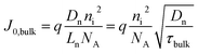
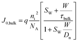
For mc-Si solar cells, the bulk lifetime of minority carriers is strongly influenced by the density of trap-assisted Shockley–Read–Hall (SRH) recombination centers caused by the traps created by impurities and multiple crystallographic defects such as gain boundaries, precipitated impurities and dislocations. The bulk SRH recombination affects the diffusion length of minority carriers and impacts the Voc, the short-circuit current density (Jsc) and fill factor (FF). The saturation current density related to the bulk region, J0,bulk, can be written as:
| |
 | (2) |
where
q is the electron charge,
W the thickness of the solar cell,
ni the intrinsic carrier density,
Dn the electron diffusion coefficient,
SW the effective rear surface recombination velocity,
Ln the electron diffusion length, related to the bulk lifetime
τbulk by the following relationship

. As seen in Fig. S1,
† for low quality substrates with short lifetime and
Ln ≪
W, the solar cell efficiency is highly dependent on the bulk lifetime and
eqn (2) can be reduced to the following approximation:
| |
 | (3) |
However for good quality substrates, for which Ln ≫ W, the solar cell efficiency becomes less dependent on the bulk lifetime but much more sensitive to the effective rear surface recombination velocity, since eqn (2) can be simplified to:
| |
 | (4) |
Fig. S1† shows the solar cell efficiency and open-circuit voltage, as a function of the bulk lifetime. In this simulation, we assumed that the mc-Si solar cell has a thickness of 180 μm, the front side of the wafer is covered by a selective emitter, while the rear side has full-area Al-BSF. For the selective emitter, we choose J0,light = 60 fA cm−2 for the lightly-doped region and J0,heavy = 180 fA cm−2 for the heavily-doped region. For the Al-alloyed back surface field, J0,BSF = 400 fA cm−2 is selected to represent the improved BSF formed by industrial screen printing and firing process. As shown in Fig. S1,† both efficiency and Voc increase significantly when bulk lifetime increases from 1 μs to 100 μs. For a bulk lifetime of 200 μs, the Voc increases to about 634 mV, which is approximately the level of current industrial mc-Si solar cells. Further improvement of the bulk lifetime, beyond 200 μs up to 1 ms does not result in a significant improvement of the Voc or the efficiency. This is because when the bulk time increases beyond 200 μs, the recombination in the solar cell becomes dominated by the rear surface and the bulk recombination becomes relatively less important.24 To have an efficiency greater than 20% mc-Si cell, one needs to optimize the front emitter, and reduce the recombination on the rear side, for example, by the introduction of back side passivation and local contacts, like in a PERC solar cell.5 The other main loss for mc-Si solar cells comes from the front surface reflection and the imperfect light trapping. The short circuit current density can be expressed as:
| |
 | (5) |
where
q, Irr, IQE,
R,
T and
A are the element charge, wavelength dependent photon flux, internal quantum efficiency, total reflectance, transmittance though the solar cell and the parasitic absorption of the anti-reflection coating or by free-carrier absorption in heavily doped regions of the cell. Fig. S2
† shows the simulated cell efficiency as a function of
Jsc, for conventional mc-Si solar cell, when the internal carrier recombination loss is constant. While the
Jsc is usually between 34 and 36 mA cm
−2, the cell efficiency ranges between 17.0% and 17.5%. If one can improve the
Jsc over 38 mA cm
−2 with less metal coverage, lower front reflectance and better light trapping, for example by the introduction of RIE, a cell efficiency over 19% is possible.
3. Experimental
3.1 Improving multi-crystalline wafer quality by ingot growth with grain-size control
Multi-crystalline silicon wafers have a lower manufacturing cost but a higher defect density than mono-crystalline silicon wafers. To improve the quality of the mc-Si ingot, the control of the solidification process was modified, including optimization of the hot zone of the furnace, the shape of the solid melt interface, the growth rate and the distribution of temperature gradient in the solidified silicon. A batch of 500 standard conventional growth mc-Si wafers (156 × 156 mm2) with an average resistivity of 1.5 Ω cm were used as a reference and compared to a batch of 500 high-performance mc-Si wafers (156 × 156 mm2) with grain-size control and with the same average resistivity of 1.5 Ω cm. To evaluate the impact of wafer quality to the cell efficiency, all wafers were processed with the standard processing sequence as described in Fig. S3a:† saw damage removal (the mixture of 49% HF and 69% HNO3 with volume ratio at 1![[thin space (1/6-em)]](https://www.rsc.org/images/entities/char_2009.gif) :5), POCl3 diffusion (N2 1000 sccm, O2 800 sccm@750–800 °C, 70 min), Phosphorus-Silicate-Glass (PSG) removal and edge isolation, Anti-Reflection Coating (ARC) with SiNx (NH3: 1250 sccm, SiH4: 500 sccm@350–400 °C, 0.25 mbar), metallization with screen-printing (commercial paste on market) and co-firing. For the two different ingot types, the map of ingot lifetime was measured by the microwave photoconductivity decay method (μ-PCD), with a WT-2000 tool from Semilab Co. Ltd. The electrical parameters, photoluminescence (PL) images and electroluminescence (EL) images of each cell were collected.
:5), POCl3 diffusion (N2 1000 sccm, O2 800 sccm@750–800 °C, 70 min), Phosphorus-Silicate-Glass (PSG) removal and edge isolation, Anti-Reflection Coating (ARC) with SiNx (NH3: 1250 sccm, SiH4: 500 sccm@350–400 °C, 0.25 mbar), metallization with screen-printing (commercial paste on market) and co-firing. For the two different ingot types, the map of ingot lifetime was measured by the microwave photoconductivity decay method (μ-PCD), with a WT-2000 tool from Semilab Co. Ltd. The electrical parameters, photoluminescence (PL) images and electroluminescence (EL) images of each cell were collected.
3.2 Implement of SE structure
In the second experiment to evaluate the impact of the implementation of the selective emitter (SE) structure, a batch of mc-Si wafers (average resistivity 1.5 Ω cm, size 156 × 156 mm2) was divided into two groups of 500 wafers each. With the exception of the different emitter structure, both groups of wafers had the same cell fabrication process as shown in Fig. S3b† for the SE solar cells and in Fig. S3a† for the reference batch. After a standard acid texturing, POCl3 is diffused onto the surface with a sheet resistance of 30 to 50 Ω square−1, then the contact area is masked with an ink material. The uncovered area is etched back in an acidic solution to reach a desired sheet resistance of 100 to 120 Ω square−1. The mask material is removed during the PSG removal and edge isolation processing. The surface concentration of phosphorus was measured by the Electrochemical Capacitance-Voltage (ECV) profiling method before and after etch back. The correlation between the cell conversion efficiency and different values of the initial or post-etching sheet resistance was studied. The cell electrical parameters such as Jsc, Voc and FF were measured.
3.3 Reduction of reflectivity by using RIE texture
As described above, RIE texturing can further reduce the light reflectance of a solar cell. This is particularly important for mc-Si cell. To investigate the impact of RIE texturing on the cell performance in comparison to the conventional acidic texturing, a batch of mc-Si wafers (resistivity 1.5 Ω cm, size 156 × 156 mm2) was divided into two groups of 500 wafers each. Both groups of wafers have the same cell fabrication process except the different texturing step as descripted in Fig. S3c† for the RIE-treated cells and in Fig. S3a† for the reference batch. After the saw damage removal in acid, RIE with a gas mixture of SF6/Cl2/O2 at a flow ratio of 2500 sccm: 1200 sccm: 2800 sccm was performed in a mass-production compatible RIE system at 0.25 mbar pressure. The plasma was excited by radio frequency (RF) at 13.56 MHz. The etching time varied from 50 to 120 second (s) to achieve different surface reflectivity. Following the plasma RIE, the RIE-induced damage layer is removed by a damage removal clean (DRC) process in a HF:HNO3 solution. The DRC time was varied to balance the loss in Voc and Jsc to achieve the highest efficiency.
4. Results and discussion
4.1 Improving the quality of multi-crystalline wafers with the optimized thermal field
As shown in Fig. 1a, the thermal field of the directional solidification system was optimized using the commercial CGSim (crystal growth simulator) program package provided by STR company, which can predict the geometry of the melt/crystal interface.25,26 And one kind of commercial raw mc-Si feedstock with granular shape was used as the seed. With optimized thermal filed and seed-assisted ingot growth, the solidification interface can be improved, the residual thermal stress in the crystal can be decreased and the grain-size can be well controlled.27 The experimental growth of ingots was produced in an industrial-furnace (GT DSS 450) with two different crystallization programs, one of which is a standard baseline process and the other is an advanced grain-size controlled growth. Fig. 1b and c show the μ-PCD lifetime mapping of the two ingots produced with the two types of growth methods. The Semilab μ-PCD gives a good qualitative assessment of the quality of the ingot. Red and yellow zones represent the area of the ingot with a high density of defects, large densities of impurities and dislocations. The blue zones represent the area of the ingot with a lower defect density and higher minority carrier lifetime. As seen in Fig. 1b, the minority carrier lifetime in the baseline ingot degrades in the top part of the ingot due to the formation of a high density of dislocations, compared to the better quality of the grain-size controlled ingot (Fig. 1c) which presents a much more uniform blue zone.
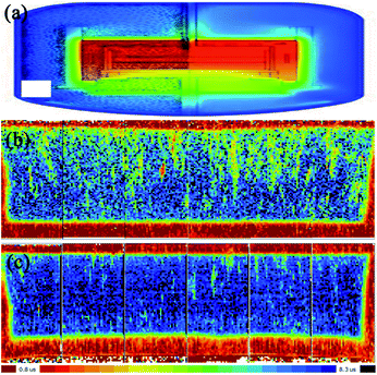 |
| | Fig. 1 (a) Distribution of optimized thermal field (GT DSS 450), longitudinal μ-PCD lifetime mapping of ingots from (b) conventional growth and (c) grain-size controlled growth. | |
To characterize the quality of the mc-Si wafers, several wafers selected from different positions (bottom, middle and top) in the ingot were analyzed by photo-luminescence (PL). As shown in Fig. S4,† the defect density in wafers extracted from different positions of the ingot with grain-size controlled growth (Fig. S4b†) is more uniform than that in wafers extracted from conventional growth ingot (Fig. S4a†). Although the defect density in the wafers at the bottom of the baseline ingot is similar to the defect density in the wafers of the ingot with grain-size control, the defect density, mostly due to the multiplication of dislocations, increases rapidly when the solidification progresses to the top of the ingot. A detailed data comparison of the defect density can be found in our previous reports.27 To further understand how the wafer quality impacts the solar cell electrical performance, PL images of both types of wafers before cell processing were compared to electro-luminescence (EL) images of the same wafers after cell. The defect density exhibits a decrease from 16.13% in conventional ingot wafers to 6.5% in grain-size controlled ingot growth wafers (Fig. S5a and S5c†). Some strong recombination centers, such as dislocation clusters, small grain boundaries, or metal precipitates, still exist and can be seen clearly in the corresponding EL image after cell process, as shown in Fig. S5b and S5d.†
In comparison to the wafers with a standard growth, there is an absolute efficiency gain of 0.38% in average obtained with the wafers with the grain-size controlled growth. The higher quality wafers lead to an improvement of an approximately 6 mV increase in Voc and 0.22 mA cm−2 increase in Jsc on average, as displayed in Table S1.† And the standard deviations of cell efficiency and electrical parameters including Voc and Jsc are more convergent due to the more uniform distribution of defect density from the bottom to top of grain-size controlled growth ingot. From the higher Voc and Jsc values, it can be concluded that the wafers with the grain-size controlled growth have fewer recombination centers than that of standard wafers. As indicated in Fig. 2, the reflectivity of solar cells made with both types of wafers is almost identical, but an approximate 2% to 7% increase in IQE can be observed in the wavelength range from 750 nm to 1050 nm, which confirms that the bulk effective carrier lifetime has been improved in the wafers fabricated with a grain-size controlled growth.
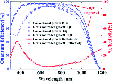 |
| | Fig. 2 IQE, external quantum efficiency (EQE) and reflectivity of cells made with different types of wafers. | |
4.2 SE structure enhanced short wavelength response
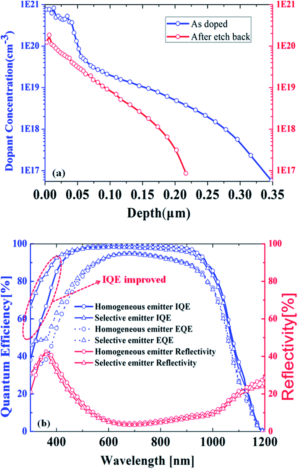
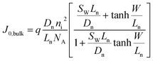
4.2.1 The characterization of surface concentration and IQE performance of SE structure. Typical industrial emitter of conventional solar cells are homogeneously doped with a surface concentration of phosphorus dopant of 8 to 10 × 1020 atoms cm−3 to achieve a relatively appropriate contact resistance. Such a conventional homogeneous emitter presents a low collection efficiency due to the high recombination rate near the surface and has a relatively low IQE performance in the short wavelength range. By comparison, solar cells with a selective emitter show excellent emitter collection properties which can be attributed to the lower surface dopant concentration and a better surface passivation after SiNx coating. In addition, the emitter recombination parameter, J0,front, is reduced in both passivated and contacted regions, resulting in higher Voc. Fig. 3a shows the emitter doping profile, measured by the Electrochemical Capacitance-Voltage (ECV) method, of emitter samples, as doped and after etch back. The surface concentration after etched back can be reduced from 8.2 × 10²⁰ (blue) to 1.2 × 10²⁰ atoms cm−3 (red), resulting in an increase in IQE from 38% to 67% at a wavelength of 300 nm, as displayed in Fig. 3b. These profiles in Fig. 3a seem not symmetric along the tail as the etch-back emitter originated from the as-diffused emitter. Because the ECV profiles are measured on different multi-crystalline silicon wafers with texture which were randomly picked up after diffusion and after etch-back process from mass production line. As illustrated in Fig. S6,† the etch-backed thickness of emitter is about 40–50 nm after checked with non-textured monocrystalline wafers and the profile after etch-back is quite close to the tail of as-diffused due to less impact from surface texture and crystal defect such as boundaries and dislocations.
 |
| | Fig. 3 (a) Phosphorus dopant concentration as a function of depth for as doped (blue) and after etch back (red) by ECV, (b) comparison of IQE between homogeneous emitter (cycle) and selective emitter (triangle). | |
4.2.2 The optimization of initial and post-etchback sheet resistance for SE structure. In order to investigate the impact of the initial sheet resistance of the emitter on the cell efficiency, the cell electrical parameters such as Jsc, Voc and FF were collected with different initial sheet resistance. It is noted that all the non-masked areas after etch back are at the same level sheet resistance around 110 Ω □−1. Fig. 4a and Table S2† show that the efficiency firstly increases then decreases with an increase of the initial sheet resistance from 40 Ω □−1 to 60 Ω □−1 and the standard deviation of 60 Ω □−1 condition is a little bigger than other two conditions, which is probably attribute to the larger variation of FF caused by initial sheet resistance. In the second experiment, the time of the etchback process is varied to achieve different post-etchback sheet resistance from 90 Ω □−1 to 130 Ω □−1 while the initial sheet resistance of 50 Ω □−1 is kept constant. The average electrical performances of the solar cells are listed in Table S3.† As shown in Fig. 4b, the cell efficiency decreases with the increasing post-etchback sheet resistance, which is because the higher post-etchback sheet resistance results in a larger series resistance, a lower FF and a bigger standard deviation of cell efficiency.
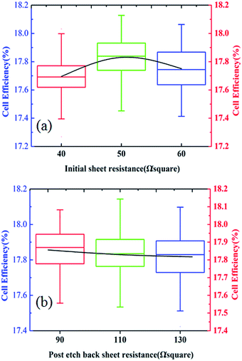 |
| | Fig. 4 Efficiency of cells with a selective emitter as a function of (a) the initial sheet resistance and (b) the post-etchback sheet resistance. | |
One thousand high-performance mc-Si wafers from ingots grown with grain-size control were divided into two groups. A SE processing sequence was applied for one group (Fig. S3b†) and the other followed the standard cell fabrication process (Fig. S3a†) as a reference. As illustrated in Table S4,† there is an absolute efficiency improvement of 0.35%, an increase of 3.3 mV in Voc, 0.61 mA cm−2 in Jsc and 0.09% in FF for the selective emitter group compared to the reference group. The higher Voc comes from less recombination in the lightly doped emitter region between the fingers.28,29 The rise in Jsc originates from the better IQE performance at short wavelengths due to the lower surface phosphorus concentration and the higher FF is attributed to the good ohmic contact between the metal grid and the heavily doped emitter underneath of contact grid.
4.2.3 The solution of misalignment between highly doping regions and metal grids in a large scale production line. As mentioned in the introduction, the key to a selective emitter structure is to form the highly and lowly doping surface concentration underneath the metal grid regions and non-metallized regions, respectively. However, it is more critical to align the metal grids with highly doping regions precisely to enable the advantage of selective emitter during the screen-printing process. From Fig. 5 and Table 1, it can been seen that once misalignment occurred between metal grids with highly doping regions, i.e., metal grids was totally or partially located on the lowly doping regions, the series resistance of solar cells increased dramatically because the ohmic contact between metal and silicon substrate can't be formed due to low doping surface concentration, resulting in a FF drop of 12% and an absolute efficiency loss of 3%. The P–N junction even could be fired-through during the co-firing process in worse case.
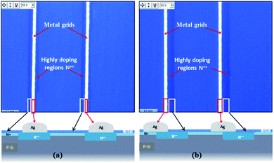 |
| | Fig. 5 (a) Well aligned between metal grids with highly doping regions, (b) misaligned between metal grids with highly doping regions. | |
Table 1 The cell electrical parameters of different solar cells: well aligned and misaligned between metal grids and highly doping regions
| |
Jsc, (mA cm−2) |
Voc, (mV) |
FF, (%) |
Rs, (Ω) |
Eff., (%) |
| Well aligned |
636.8 |
36.74 |
79.38 |
0.002 |
18.57 |
| Misaligned |
633.2 |
36.32 |
67.71 |
0.012 |
15.59 |
For an experiment in a laboratory research, the metal grids and highly doping surface concentration regions could be aligned carefully by manual operation. However, it is very difficult to do so in a large-scale mass production line and the misalignment happens frequently, which is the key reason why the SE can't be implemented in a large-scale production line although the SE concept had been invented for many years. It was found that the vendors of mask formation equipment and metal grid printing equipment are from different countries, the engineers never talked each other and they used different alignment mode respectively. After many studies, the align algorithm was finally unified as edge-align mode for both mask formation and metal grid printing to ensure that the printed patterns were located in the middle of the wafers. The misalignment issue was solved successfully in a large-scale mass production line.
4.3 Result of RIE process optimization and implementation
4.3.1 Reflectivity varying test and micro surface comparison. RIE is used to create microscopic ridges on the surface of the solar cell. Ridged surface enhances the conversion efficiency by reducing the light reflectance of the front surface which allows more sunlight to be absorbed. Compared to a surface reflectivity of ∼23% for conventional acid texturing, the surface reflectivity of RIE-treated silicon surface can be reduced to approximately 6% (Fig. 6a) due to the formation of pyramidal-like texturing. As displayed in Table S5,† when no DRC is applied after RIE, only a small absolute efficiency gain of 0.22% can be achieved and a 2 mV loss in Voc can be observed due to a significant surface damage induced by plasma bombardment on the wafer surface and the sharp feature of the surface texturization. Fig. 6b shows IQE of RIE and acid textured mc-Si solar cells between wavelengths ranging from 400 nm to 900 nm. The IQE of RIE textured cells is lower than that of the acid textured cells, which clearly reveals that either the RIE process introduces surface damage or the sharply textured surface is detrimental to surface passivation, in both cases leading to an enhanced carrier recombination at the front surface and poor IQE, which degrades the electrical properties, especially Voc. The average surface reflectance of 9%, 6%, and 4% were obtained with a varying texturing time of 50 s 70 s and 120 s respectively, as shown in Fig. 6c.
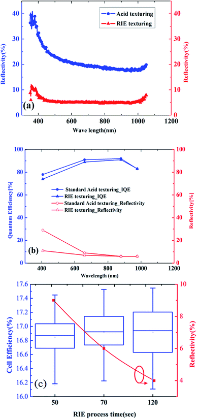 |
| | Fig. 6 (a) Reflectivity of bare silicon surface after RIE texturing process compared to acid texturing, (b) IQE and reflectance of solar cell with RIE without DRC vs. acid texturing, (c) reflectivity and cell efficiency vs. RIE process time. | |
For an experiment in a laboratory research, reducing RF power is one of the methods to minimize the side effect of surface damage induced by the plasma. However, it is not practical to do so in a mass production line, since lower RF means lower etch rate and lower throughput. In this work, to avoid a decrease in Voc from the plasma induced surface damage, a DRC process was performed for 20 s in a mixture solution of HF:HON3 at 1:10 with a buffering additive to keep the constant etch rate and maintain the etch uniformity from batch to batch. As listed in Table S6,† compared to the acid texturing group, there is an average efficiency gain of 0.38% to 0.46% absolute for all RIE processed groups, the efficiency increases with reflectance decrease. The efficiency stays almost constant when the reflectance is lower than 6% as shown in Fig. 6c. However, the standard deviation of cell efficiency is getting bigger with RIE process time increasing.
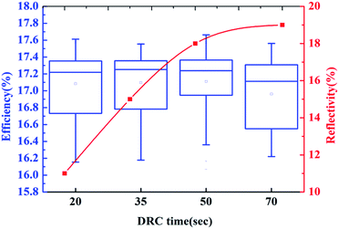
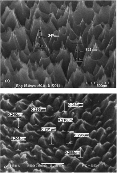
4.3.2 Tuning the DRC time. In our experiment, the post-RIE reflectance was fixed at 6% while the DRC time was varied. The DRC process removes the surface damage induced by the RIE plasma bombardment and rounds the sharp features of the textured surface, which are the cause of Voc loss due to enhanced surface recombination. Longer DRC times degrade the texturization and increase the front surface reflectance (Fig. 7, red). During the DRC process, the sharp pyramidal-like structure on the textured surface is rounded (Fig. 8) and smoothed. The height of textured structure is reduced from 321–347 nm to 205–298 nm after the DRC process, which is needed for high quality surface passivation after the SiNx ARC process and reduction of Voc loss. As indicated in Table S7,† Voc increases with increasing DRC process time due to the reduced surface recombination and Jsc decreases due to a higher reflectance. Therefore, the loss of Voc and Jsc needs to be balanced by optimizing DRC to achieve the highest solar cell conversion efficiency. The cell efficiency exhibits a maximum for DRC processing times between 20 and 50 s (Fig. 7, blue) and the standard deviation of cell efficiency is getting bigger when DRC process time increases to 70 s. The condition of 50 s DRC time with 18% reflectance post-DRC has the highest efficiency gain of 0.63% in comparison to the reference group of acid textured solar cells.
 |
| | Fig. 7 The reflectivity and cell efficiency vs. DRC time. | |
 |
| | Fig. 8 SEM pictures of the RIE textured silicon surface before (a) and after (b) DRC process. | |
4.4 Multiple process combination tests
Once all individual processes were optimized, an integration of the multiple technologies was performed. Grain-size controlled ingots were fabricated to obtain high-performance mc-Si wafers. The following solar cell process was selected: saw damage removal, RIE texturing followed by DRC 50 s, POCl3 diffusion (N2 1000 sccm, O2 800 sccm@750–800 °C, 70 min), selective emitter formation, PECVD SINx (NH3: 1250 sccm, SiH4: 500 sccm@350–400 °C, 0.25 mbar), metal screen printing, co-firing. A reference group of cells fabricated with the baseline process and standard wafers was used for comparison (Fig. 3a). As listed in Table S8,† with the optimized process the maximum achieved efficiency is 18.84% (Fig. 9a) with batch average efficiency of 18.65% over more than 9000 solar cells. Each of the cell parameters (Jsc, Voc, and FF) has been improved compared to the standard solar cells; in particular, a 1.58% of absolute efficiency gain is achieved. 60 solar cells with an efficiency of 18.65% in average were assembled into a 1650 × 990 mm2 module and tested under the Standard Test Condition (STC) at the State Key Lab of Photovoltaic Science and Technology, the maximum module power output reached 270.3 W (Fig. 9b) i.e. a 20 W power gain compared to a typical value of 250 W for conventional mc-Si modules of the same dimensions.
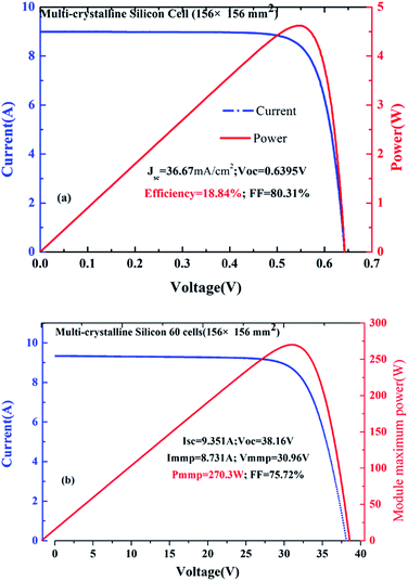 |
| | Fig. 9 I–V curve of (a) champion solar cell and (b) 270.3 W module power performance. | |
5. Conclusions
Low-defect density mc-Si ingots were successfully grown by optimizing the hot-zone, solidification process recipes and controlling the grain size with a seeded nucleation technology, which leads to a batch-average improvement of 6 mV in Voc, 0.22 mA cm−2 in Jsc and 0.38% absolute in efficiency. SE structure with a precise alignment between highly doping regions and metal grids was successfully implemented, decreasing the surface concentration of phosphorus dopant from 8.2 × 10²⁰ to 1.2 × 10²⁰ atom cm−3, resulting in an improvement of the IQE from 38% to 67%, accompanying with an increase of the open circuit voltage of 3 mV and the conversion efficiency of 0.35%. A DRC process is found to be an effective way to remove the surface damage induced by RIE plasma bombardment, which results the efficiency gain up to 0.63% with RIE texturing. After incorporating these several practical advanced technologies on a mass production line, the average efficiency of 18.65% was demonstrated while the maximum conversion efficiency was 18.84% over a batch of 10000 solar cells, equating to an absolute efficiency gain of 1.58% compared to a conventional solar cell. The corresponding module power was 270.3 W, a 20 W increase over a conventional 60-cell mc-Si module of the same dimensions.
Acknowledgements
Authors would like to thank Dr Pierre, Dr Yang Yang, Jing Mao, Jian Sheng, Yan Chen, Zhen Zhang and Wenhao Cai for their assistance with experiments, data collection and characterization. This work was supported by the National Natural Science Foundation of China (61474045) and Natural Science Foundation of Jiangsu Province for Young Scientist (No. BK20140273).
Notes and references
- S. Yuvarajan, D. Yu and S. Xu, A novel power converter for photovoltaic applications, J. Power Sources, 2004, 135, 327–331 CrossRef CAS.
- Y. F. Chen, Z. Q. Feng, and P. J. Verlinden, Assessment of module efficiency and manufacturing cost for industrial crystalline silicon and thin film technologies, 6th World Conference on Photovoltaic Energy Conversion WCPEC-6, Kyoto, Japan, November 2014, pp. 24–28 Search PubMed.
- L. L. Mittelstädt, S. Dauwe and A. Metz, et al. Front and rear silicon-nitride-passivated multicrystalline silicon solar cells with an efficiency of 18.1%, Progress in Photovoltaics: Research and Applications, 2002, vol. 10(1), pp. 35–39 Search PubMed.
- J. Zhao, A. Wang, M. A. Green and F. Ferrazza, 19.8% efficient multicrystalline silicon solar cells with ‘honeycomb’ textured front surface, Appl. Phys. Lett., 1998, 73, 1991 CrossRef CAS.
- O. Schultz, S. W. Glunz and G. P. Willeke, Multicrystalline Silicon Solar Cells Exceeding 20% Efficiency, Progress in Photovoltaics: Research and Applications, vol. 12, 2004, pp. 553–558 Search PubMed.
- Q. Qiao, H. Lu, J. Ge, X. Xia, R. Chen, J. Yang, J. Zhu, Z. Shi and J. Chu, 18.5% efficient AlOx/SiNy rear passivated industrial multicrystalline silicon solar cells, Appl. Surf. Sci., 2014, 305, 439–444 CrossRef CAS.
- P. J. Verlinden, W. W. Deng, X. L. Zhang, Y. Yang, Z. Xiong, J. M. Xu, Y. H. Shu, P. Quan, J. Sheng, Y. F. Chen, S. Zhang, J. Bao, F. L. Ping, Y. B. Zhang and Z. Q. Feng, Strategy, development and mass production of high-efficiency crystalline silicon PV modules, 6th World Conference on Photovoltaic Energy Conversion WCPEC-6, Kyoto, Japan, November 2014, pp. 24–28 Search PubMed.
- S. K. Srivastava, P. Singh and M. Yameen, et al. Antireflective ultra-fast nanoscale texturing for efficient multi-crystalline silicon solar cells, Sol. Energy, 2015, 115, 656–666 CrossRef CAS.
- C. W. Lan, W. C. Lan, T. F. Lee, A. Yu, Y. M. Yang, W. C. Hsu, B. Hsu and A. Yang, Grain control in directional solidification of photovoltaic silicon, J. Cryst. Growth, 2012, 360, 68–75 CrossRef CAS.
- K. Fujiwara, W. Pan, K. Sawada, M. Tokairin, N. Usami, Y. Nose, A. Nomura, T. Shishido and K. Nakajima, Directional growth method to obtain high quality polycrystalline silicon from its melt, J. Cryst. Growth, 2006, 292, 282–285 CrossRef CAS.
- N. Usami, R. Yokoyama, I. Takahashi, K. Kutsukake, K. Fujiwara and K. Nakajima, Relationship between grain boundary structures in Si multicrystals and generation of dislocations during crystal growth, J. Appl. Phys., 2010, 107, 013511 CrossRef.
- S. Würzner, R. Helbig, C. Funke and H. J. Möller, The relationship between microstructure and dislocation density distribution in multicrystalline silicon, J. Appl. Phys., 2010, 108, 083516 CrossRef.
- Y. Zhang, J. Xu and J. Mao, et al. Long-term reliability of silicon wafer-based traditional backsheet modules and double glass modules, RSC Adv., 2015, 5, 65768–65774 RSC.
- M. Z. Rahman, Status of Selective Emitters for p-Type c-Si Solar Cells, Opt. Photonics J., 2012, 2, 129–134 CrossRef CAS.
- I. B. Cooper, K. Tate, J. S. Renshaw, A. F. Carroll, K. R. Mikeska, R. C. Reedy and A. Rohatgi, Investigation of the mechanism resulting in low resistance Ag thick-film contact to Si solar cells in the context of emitter doping density and contact firing for current-generation Ag paste, IEEE Journal of Photovoltaics, 2014, 4, 134–141 CrossRef.
- V. Shanmugam, J. Cunnusamy, A. Khanna, P. K. Basu, Y. Zhang, C. Chen, A. F. Stassen, M. B. Boreland, T. Mueller, B. Hoex and A. G. Aberle, Electrical and microstructure analysis of contact formation on lightly doped phosphorus emitters using thick-film Ag screen printing pastes, IEEE Journal of Photovoltaics, 2014, 4, 168–174 CrossRef.
- S. Zhong, W. Shen, F. Liu and X. Li, Mass production of high efficiency selective emitter crystalline silicon solar cells employing phosphorus ink technology, Sol. Energy Mater. Sol. Cells, 2013, 117, 483–488 CrossRef CAS.
- Z. Liang, F. Zeng, H. Song and H. Shen, Effect of porous Si and an etch-back process on the performance of a selective emitter solar cell, Sol. Energy Mater. Sol. Cells, 2013, 109, 26–32 CrossRef CAS.
- W. A. Nositschkaa, O. Voigt, P. Manshanden and H. Kurz, Texturisation of multicrystalline silicon solar cells by RIE and plasma etching, Sol. Energy Mater. Sol. Cells, 2003, 80, 227–237 CrossRef.
- D. Muriasa, C. Reyes-Betanzo, M. Morenoa, A. Torres, A. Itzmoyotl, R. Ambrosio, M. Soriano, J. Lucas and P. R. Cabarrocas, Black Silicon formation using dry etching for solar cells applications, J. Mater. Sci. Eng. B, 2012, 177, 1509–1513 CrossRef.
- S. K. Srivastava, D. Kumar and Vandana, et al. Silver catalyzed nano-texturing of silicon surfaces for solar cell applications, Sol. Energy Mater. Sol. Cells, 2012, 100, 33–38 CrossRef CAS.
- J. Yoo, Reactive ion etching (RIE) technique for application in crystalline silicon solar cells, Sol. Energy, 2010, 84, 730–734 CrossRef CAS.
- Y. Inomata, K. Fukui and K. Shirasawa, Surface texturing of large area multicrystalline silicon solar cells using reactive ion etching method, Sol. Energy Mater. Sol. Cells, 1997, 48, 237–242 CrossRef CAS.
- Y. F. Chen, H. Shen and P. P. Altermatt, Analysis of recombination losses in screen-printed aluminum-alloyed back surface fields of silicon solar cells by numerical device simulation, Sol. Energy Mater. Sol. Cells, 2014, 120, 356–362 CrossRef CAS.
- O. V. Smirnova, et al. Optimization of furnace design and growth parameters for Si Cz growth using numerical simulation, J. Cryst. Growth, 2008, 310, 2185–2191 CrossRef CAS.
- Website of STR, http://www.semitech.us, Last accessed January 2nd, 2016.
- Z. Zhang, Y. Zhang, Z. Xiong, H. Ye, F. Ping, S. Fu, Z. Feng and P. J. Verlinden, Growth of low defect density mc-Si ingots and wafers for PV, Proceedings of the 40th IEEE Photovoltaic Specialists Conference, Denver, CO, 2014, pp. 3043–3045 Search PubMed.
- J. Tao, J. Liu, L. Chen, H. Cao, X. Meng, Y. Zhang, C. Zhang, L. Sun, P. Yang and J. Chu, 7.1% efficient co-electroplated Cu2ZnSnS4 thin film solar cells with sputtered CdS buffer layers, Green Chem., 2016, 18, 550–557 RSC.
- J. Tao, K. Zhang, C. Zhang, L. Chen, H. Cao, J. Liu, J. Jiang, L. Sun, P. Yang and J. Chu, Chem. Commun., 2015, 51, 10337–10340 RSC.
Footnote |
| † Electronic supplementary information (ESI) available: Experimental, simulated cell efficiency, different cell fabrication processes, PL mapping. See DOI: 10.1039/c6ra05765a |
|
| This journal is © The Royal Society of Chemistry 2016 |


 . As seen in Fig. S1,† for low quality substrates with short lifetime and Ln ≪ W, the solar cell efficiency is highly dependent on the bulk lifetime and eqn (2) can be reduced to the following approximation: