
 Open Access Article
 This Open Access Article is licensed under a Creative Commons Attribution-Non Commercial 3.0 Unported Licence
Quality of graphene on sapphire: long-range order from helium diffraction versus lattice defects from Raman spectroscopy†
Gloria
Anemone
a,
Esteban
Climent-Pascual
b,
Hak Ki
Yu
cd,
Amjad
Al Taleb
a,
Felix
Jiménez-Villacorta
b,
Carlos
Prieto
b,
Alec M.
Wodtke
cd,
Alicia
De Andrés
b and
Daniel
Farías
*aef
aDepartamento de Física de la Materia Condensada, Universidad Autónoma de Madrid, 28049 Madrid, Spain. E-mail: daniel.farias@uam.es
bInstituto de Ciencia de Materiales de Madrid, Consejo Superior de Investigaciones Científicas, Spain
cInstitute for Physical Chemistry, University of Göttingen, 37077 Göttingen, Germany
dMax Planck Institute for Biophysical Chemistry, 37077 Göttingen, Germany
eInstituto “Nicolás Cabrera”, Universidad Autónoma de Madrid, 28049 Madrid, Spain
fCondensed Matter Physics Center (IFIMAC), Universidad Autónoma de Madrid, 28049 Madrid, Spain
First published on 12th February 2016
Abstract
We report a new method to produce high-quality, transparent graphene/sapphire samples, using Cu as a catalyst. The starting point is a high-quality graphene layer prepared by CVD on Cu(111)/Al2O3. Graphene on sapphire is obtained in situ by evaporation of the Cu film in UHV. He-diffraction, atomic force microscopy (AFM), Raman spectroscopy and optical transmission have been used to assess the quality of graphene in a metal free area. We used helium atom scattering as a sensitive probe of the crystallinity of the graphene on sapphire. The observation of high reflectivity and clear diffraction peaks demonstrates the presence of flat and homogeneous graphene domains over lateral scales of microns, consistent with the AFM results. Surprisingly, putting graphene on sapphire improves the quality of the He-diffraction spectra. Graphene forms a moiré pattern with a (11 × 11) periodicity, aligned with the (1 × 1) sapphire unit cell. The lattice constant of graphene on sapphire is a = (2.44 ± 0.02) Å. The phonon dispersion of the graphene flexural mode has been measured. This allowed the determination of the bending rigidity k = 0.61 ± 0.15 eV, and the graphene–sapphire coupling strength g = (5.8 ± 0.4) × 1019 N m−3. The uniformity of the graphene has also been investigated by Raman mapping. Judging by the ratio of the 2D to G peaks, the quality of the graphene is not degraded by Cu removal. The high transparency (80%) measured in the visible range makes this system suitable for many applications that require hybrid properties commonly associated with metals (conductivity) and insulators (transparency). Our study shows that He-diffraction and Raman provide crucial information on quite different, complementary aspects of the same samples.
Introduction
Presently, great effort is being expended to find a suitable replacement for the industry standard transparent conductors in use. This effort is motivated by the fact that these materials require scarce metals (like in indium tin oxide, ITO), perform poorly on flexible substrates and require expensive vacuum deposition techniques.1,2 Reducing the cost of transparent conductors, moving away from elements that are expensive and/or in short supply, is crucial for the future.3,4 Graphene/sapphire samples may provide a possible alternative to these materials for many applications. However, most of the available methods for controlled and scalable preparation of graphene (Gr) on metallic substrates cannot be easily extended to grow Gr on sapphire. The standard method to obtain Gr is by chemical vapor deposition (CVD) on metallic foils, mostly copper and nickel, which serve as catalysts for the dissociation of the precursor gas (typically methane or ethylene) to form the Gr layer. An important drawback is the necessity to eliminate the metallic foil before transferring the Gr layer to substrates adequate for its implementation in devices, in general either transparent substrates or silicon. The metal elimination is performed by using acids, which leads to the appearance of residues in the Gr layer. So far, most of the methods reported have not produced Gr layers of quality comparable to that obtained for instance on Cu.5–9 Typically, the Raman D-peak (related to the presence of defects) is larger than the G-peak, indicating small grain size (∼15 nm). For Gr on sapphire, a few methods have been reported in which the Raman D-peak was significantly reduced; these methods are either based on the high-temperature (1500–1600 °C) decomposition of the precursor gas without using a metal catalyst10,11 or by direct CVD growth on dielectric surfaces by simultaneously dewetting the Cu film.12 Even though some of these samples exhibit excellent performances, like a room-temperature Hall mobility of 2.000 cm2 V−1 s−1,10 it is interesting to explore alternative ways of producing similar samples.Here we report a new method to produce high quality, transparent Gr/sapphire samples in UHV. The starting point is a high-quality Gr layer prepared by CVD using Cu as a catalyst.13 The samples are then transferred to UHV, where the Cu film is evaporated. The samples have been characterized by helium atom scattering (HAS), Raman spectroscopy and atomic force microscopy (AFM). HAS is an established means of investigating the structure and dynamics of insulating as well as conducting surfaces in a completely nondestructive manner.14 HAS diffraction provides direct information on surface crystallinity, and HAS specular scattering is highly sensitive to surface flatness and defect density.15 Since He beams are typically 1 mm in size, the method provides information over a macroscopic region. Therefore, HAS is an excellent complement to Raman spectroscopy, which provides information on the quality of the Gr layer over length scales of 1 μm. HAS has been already used to characterize Gr grown on several metal substrates.16–19 Our current study reports the first systematic comparison of HAS with Raman results.
Our study shows that the observation of clear He-diffraction features, which points to the existence of large Gr domains over a macroscopic region (of the order of a few microns), may be consistent with the simultaneous observation of large Raman D-peaks arising from regions on the surface not large enough to produce diffraction peaks. Finally, our approach presents several advantages with respect to previous reported methods, like a high transparency (80%) in the visible range, a short preparation time (30 minutes) and the use of a moderate preparation temperature (∼900 °C). Finally, our method has the great advantage of being performed in UHV, leaving the Gr surface free of contaminants.
Experimental
Sample preparation
The starting point is a high-quality Gr layer prepared by CVD on Cu(111) grown on α-Al2O3(0001) (c-plane sapphire). The growth of Cu film on c-plane sapphire was achieved by using the electron beam evaporation method, as reported in our previous study,13 except for the total thickness (1000 nm) and growth rate (0.3 nm s−1). Different initial thicknesses of Cu(111) films have been used for Gr growth in order to improve the quality of the Gr layer and the elimination of Cu without Gr film deterioration. The best results have been obtained with a 1000 nm thick Cu film. For comparison, results corresponding to a sample with a lower thickness (500 nm) are summarized in the ESI.† The samples were prepared by CVD in Goettingen13 and then transported to Madrid to complete the preparation in a UHV chamber with base pressure in the low 10−10 mbar range; typically, the samples were exposed to ambient conditions for one week before being introduced into the UHV scattering chamber for He diffraction. Once in UHV, the samples were annealed at 800 K with 2 × 10⁻⁷ mbar of C2H4. This treatment leads to a significant improvement in surface quality, as indicated by the increase of the He-specular intensity.20 Graphene on sapphire has been obtained in situ by evaporation of the Cu film in UHV, heating the samples at 1150 K for 30 min. The sample temperature was measured with a type-C thermocouple spot-welded to the sample holder. The sample preparation steps are schematically illustrated in Fig. 1.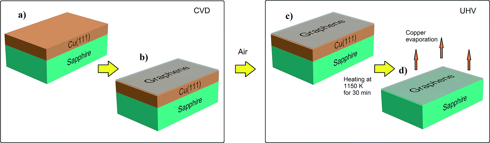 | ||
| Fig. 1 Schematic procedure for the Gr growth on sapphire. (a) Copper is deposited on c-plane (0001) sapphire by electron beam evaporation. (b) Graphene growth on copper by CVD. (c) Afterexposure to ambient conditions, the sample was introduced into the He-scattering UHV chamber. (d) After heating up in UHV, Cu evaporates, leaving a Gr layer deposited on the sapphire substrate. | ||
Results and discussion
Helium atom scattering
The angular distributions presented in this work were measured after aligning the sample along the direction of the dominant Gr orientation (80%), which corresponds to the [
![[2 with combining macron]](https://www.rsc.org/images/entities/char_0032_0304.gif) 11] direction of the Cu(111) underneath. The remaining 20% of the sample is covered by domains rotated 30° with respect to the [11] direction.20 In the following, after discussing the shapes of specular peaks we analyze the structures corresponding to the measured diffraction peaks.
11] direction of the Cu(111) underneath. The remaining 20% of the sample is covered by domains rotated 30° with respect to the [11] direction.20 In the following, after discussing the shapes of specular peaks we analyze the structures corresponding to the measured diffraction peaks.
Fig. 2a shows a comparison of angular distributions of He atoms scattered from Gr/Cu/Al2O3 (red) and Gr/Al2O3 (black). The high specular reflectivity and the presence of diffraction peaks demonstrate the existence of a well-ordered Gr layer, with a low density of defects, over areas of the order of the beam size (ca. 1 mm). However, the width of the specular peak of Gr/Al2O3 FWHM = 0.14°, which corresponds roughly to the angular resolution of the HAS machine, is lower than that of Gr/Cu/Al2O3 FWHM = 0.56°. The width of the specular peak depends on the quality of the surface and gives information about the domain size w through the relationship FWHM 1/w.21 Therefore, the above comparison can lead to the counterintuitive interpretation that the Gr layer exhibits larger domains after the copper removal. However, this is not the case as we find by comparing the surfaces of Al2O3 and Cu/Al2O3. The latter has been obtained by removing the Gr layer in Gr/Cu/Al2O3 through Ar+ sputtering, followed by annealing at 940 K. The corresponding angular distributions are shown in the ESI (Fig. SI1†). Further heating at 1150 K for 30 min led to obtaining the clean Al2O3 surface. The obtained peak widths are FWHM = 0.56° and 0.27° for Cu/Al2O3 and Al2O3, respectively. This clearly shows that the FWHM of the Gr covered surface is determined mainly by the substrate underneath. The width of the specular peaks of Gr/Cu/Al2O3 and Cu/Al2O3 are almost identical. A possible explanation is that the Cu film is terminated by a corrugated surface, which may induce an additional broadening of the specular peak.
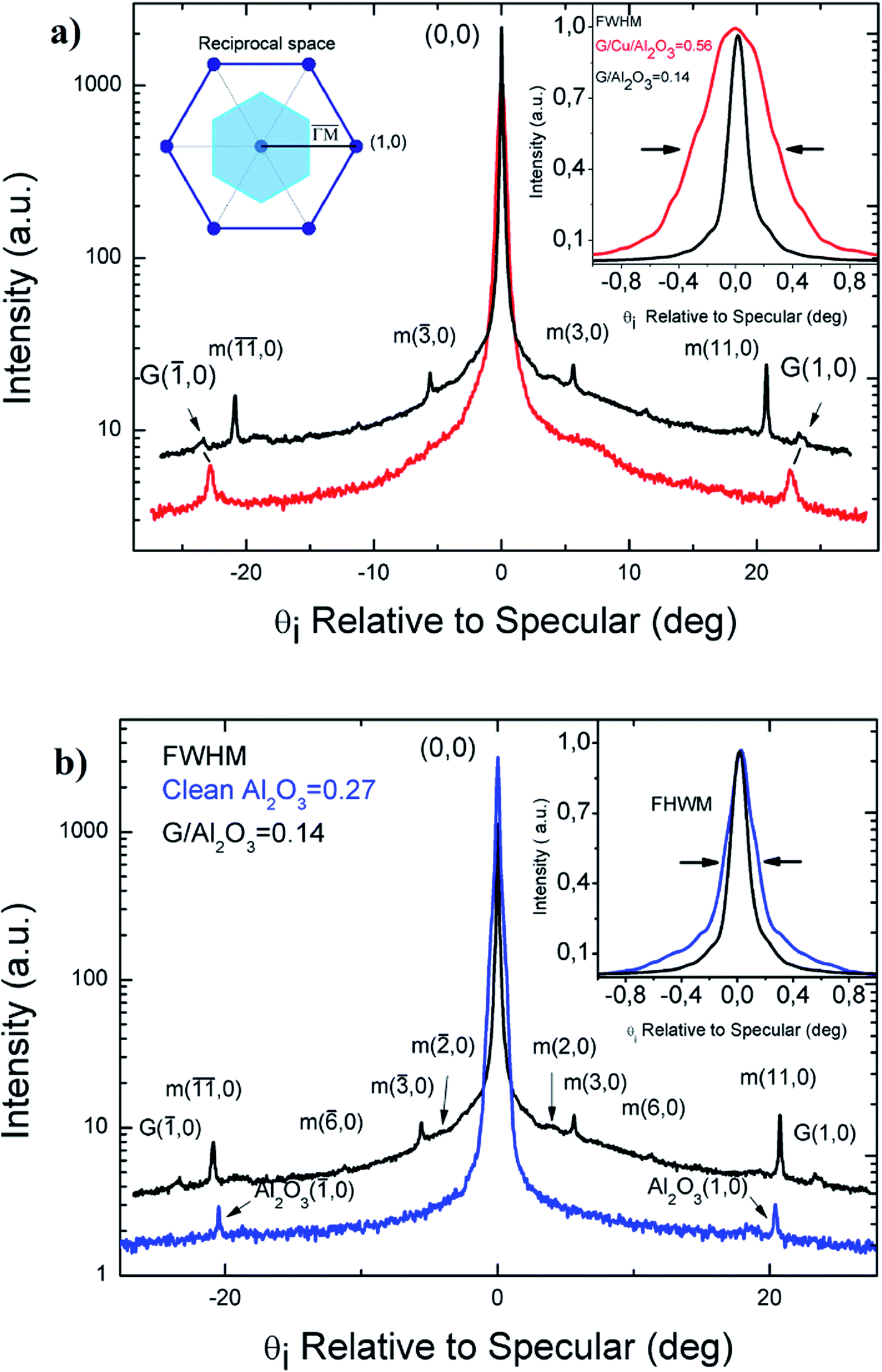 | ||
Fig. 2 (a) Angular distributions of He atoms scattered from Gr/Cu/Al2O3 (red spectrum) and Gr/Al2O3 (black spectrum) along  . (b) Comparison of He diffraction spectra from Gr/Al2O3 (black) and clean Al2O3 (blue). The sample temperature is 90 K, and the He-incident energy is Ei = 19.8 meV (the small shift in the position of first order peaks is a result of quite small differences in the He beam energy). The inset on the right side shows a detailed view of the profile of the specular peaks. The diffraction peaks of the moiré superstructure are labelled as “m(n,0)”. . (b) Comparison of He diffraction spectra from Gr/Al2O3 (black) and clean Al2O3 (blue). The sample temperature is 90 K, and the He-incident energy is Ei = 19.8 meV (the small shift in the position of first order peaks is a result of quite small differences in the He beam energy). The inset on the right side shows a detailed view of the profile of the specular peaks. The diffraction peaks of the moiré superstructure are labelled as “m(n,0)”. | ||
On the other hand, a comparison of HAS angular distributions from Al2O3 and Gr/Al2O3 (Fig. 2b) shows a decrease of the FWHM by 50% in the Gr covered surface, which points to the formation of larger domains. The inset in Fig. 2b shows the normalized specular peaks in a linear scale, where a quasi-triangular background appears around the specular peaks and is especially pronounced in the Al2O3 spectrum. Previous HAS studies have shown that the presence of a triangular background in the vicinity of the specular peak is the signature of a random distribution of defects.22 Similar conclusions have been obtained in a more recent study reported by Manson et al.23 Therefore, we conclude that scattering from point defects dominates in both surfaces, although to a lesser degree in the Gr covered surface. These observations suggest that the Gr layer covers like a carpet the rough and flat sapphire substrate, hiding a portion of the single defects and softening the roughness of the step edges. Even though the Gr layer certainly contains many defects, our data suggest that the Gr/Al2O3 layer exhibits a reduced number of defects, leading to an average domain size larger than that of clean Al2O3. Since the FWHM observed for Gr/Al2O3 is limited by the resolution of our system, we can conclude that the average domain size is at least one order of magnitude larger than the transfer width of our system (200 nm). The coherence length for the Al2O3 surface, which is of the same order of the size24 of the terraces is ∼40 nm. The measured absolute reflectivity of He atoms from Gr/Al2O3 is 5% at the incident conditions used in Fig. 2b. This high reflectivity combined with the narrow specular peak observed suggests that these samples are excellent candidates to be used as a focussing mirror in scanning He atom microscopy.25–27
The different diffraction peaks in the angular distributions of Fig. 2 correspond to the periodicities of the Gr, sapphire and multiple moiré superstructures resulting from the mismatch of the two surfaces. The lattice constant of Gr on sapphire has been determined from the positions of its first order diffraction peaks indicated as G(0,1) and G(![[1 with combining macron]](https://www.rsc.org/images/entities/char_0031_0304.gif) ,0) in Fig. 2a and b, using the in-plane Bragg diffraction condition for a hexagonal two-dimensional structure. The derived value a = (2.44 ± 0.02) Å is identical to the one reported for Gr/Cu(111),20 and agrees well with 2.4612 Å, the periodicity of a single carbon layer in graphite.28 The low intensity of the first order diffraction peaks points to a low corrugation of the Gr/Al2O3 surface. Well-resolved and intense first order diffraction peaks are present in the blue spectrum in Fig. 2b of the Al2O3 substrate, denoted by Al2O3(10) and Al2O3(0), appear at the positions expected for the shortest hexagonal lattice length of sapphire (Al–Al distance), a = 2.74 Å. As far as we know, this is the first He-diffraction spectrum reported from a clean sapphire surface.
,0) in Fig. 2a and b, using the in-plane Bragg diffraction condition for a hexagonal two-dimensional structure. The derived value a = (2.44 ± 0.02) Å is identical to the one reported for Gr/Cu(111),20 and agrees well with 2.4612 Å, the periodicity of a single carbon layer in graphite.28 The low intensity of the first order diffraction peaks points to a low corrugation of the Gr/Al2O3 surface. Well-resolved and intense first order diffraction peaks are present in the blue spectrum in Fig. 2b of the Al2O3 substrate, denoted by Al2O3(10) and Al2O3(0), appear at the positions expected for the shortest hexagonal lattice length of sapphire (Al–Al distance), a = 2.74 Å. As far as we know, this is the first He-diffraction spectrum reported from a clean sapphire surface.
The He-diffraction spectrum measured from the Gr/Al2O3 surface exhibits a more complex structure, due to the moiré reconstruction. The (10) diffraction peak of the atomic lattice of Gr (denoted by Gr(1,0)) is observed at 23° away from the specular peak (0,0). However, the existence of other diffraction peaks, due to the moiré superstructure, is clearly detected along the whole diffraction pattern. The angular positions of the diffraction peaks from the Gr moiré lattice are in good agreement with expected values for a hexagonal structure with a periodicity of 30 Å. In particular, the third, the sixth and the eleventh order diffraction of the moiré pattern (labelled m(3,0), m(6,0) and m(11,0)) are clearly observed in the black spectrum in Fig. 2b. A comparison of the angular positions of diffraction peaks of Gr/Al2O3 and clean Al2O3 surfaces shows that the high-intensity sharp peak m(11,0) matches exactly the position of the peak (1,0) of sapphire. Thus, we can conclude that the moiré pattern corresponds to a (11 × 11) periodicity aligned with the (1 × 1) sapphire unit cell. This is schematically shown in Fig. 3b. The moiré structure has been investigated by varying the azimuthal orientation of the sample. Fig. 3a shows several He-diffraction angular distributions. Each spectrum has been recorded after a small azimuthal rotation of the sample with respect to an axis lying in the incident plane. The black curve is the same as that shown in Fig. 2 and is denoted as 0°. Rotating the sample we can see how different peaks from the moiré pattern are detected. In the red curve, rotated by 0.5°, the peak m(11,0) disappears, whereas the m(9,0) and the m(10,0) diffraction peaks are clearly resolved. With a further rotation of 0.5° (denoted as 1°, blue curve), the measured spectrum exhibits weaker but still clear peaks for different order of diffraction (m(8,0), m(4,0) and m(2,0)). For a rotation of 1.5° (magenta curve) the peaks m(4,0) and m(2,0) are still observed, but the m(8,0) peak is not present. The green curve has been recorded for an azimuthal rotation of ∼30°. The position of the detected diffraction peaks fits the diffraction pattern produced by a Gr layer rotated by 30° with respect to the (1 × 1) sapphire unit cell, which corresponds to a  structure. The presence of shadows of the m(1,0) and m(2,0) peaks in this spectrum is due to small misalignment of the tilt angle which appears for different azimuthal orientations.
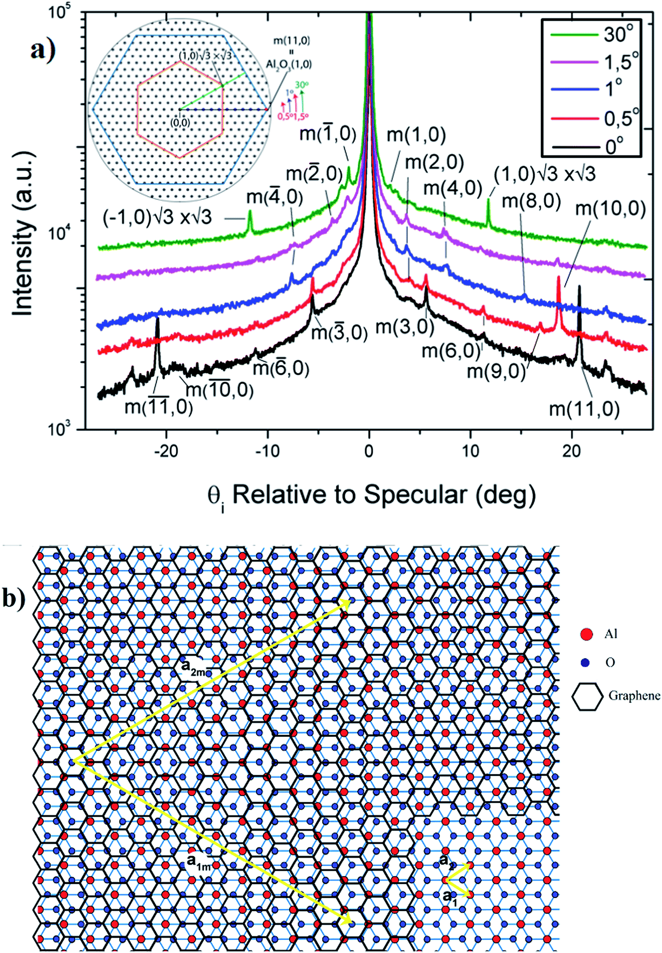 | ||
Fig. 3 (a) Angular distribution of He scattering from Gr/Al2O3 as a function of azimuthal rotation. The inset shows the directions on the moiré reciprocal lattice and the first order diffraction of the sapphire (blue hexagon) and  (red hexagon) structures. (b) Proposed model for the moiré (11 × 11) structure, which is obtained by superimposing (12 × 12) Gr honeycombs on top of (11 × 11) sapphire unit cells. The primitive vectors of the moiré (a1m and a2m) and sapphire unit cells (a1 and a2) are also shown. (red hexagon) structures. (b) Proposed model for the moiré (11 × 11) structure, which is obtained by superimposing (12 × 12) Gr honeycombs on top of (11 × 11) sapphire unit cells. The primitive vectors of the moiré (a1m and a2m) and sapphire unit cells (a1 and a2) are also shown. | ||
The diffraction patterns from the moiré superstructure indicate that the Gr/sapphire system keeps the same domain ratio (80% along the main direction, and 20% rotated 30° with respect to this direction) present in the starting system, Gr/Cu/Al2O3. We have also recorded He-diffraction spectra for intermediate azimuthal rotations, and no evidence of additional periodicities has been detected. It is interesting to compare our data with the results reported by Hwang et al.10 These authors have grown Gr on c-plane (0001) sapphire directly without metal catalysis and concluded, based on detailed spatial electron diffraction measurements and DFT calculations, that Gr on sapphire grows forming a single dominant crystal orientation for around 80% of the material. In their work, however, the orientation is determined at an early stage of the nucleation during the growth process, and therefore multiple rotational domains with respect to the substrate are obtained. The preparation method described in our current work, on the other hand, could in principle lead to the formation of only one rotational domain if the starting point, i.e. Gr/Cu/Al2O3, was formed by only one domain.
Hwang et al. also performed DFT calculations (including the van der Waals interaction) for commensurate cells with orientations of 0°, 11° and 22° with respect to the sapphire.10 From the similarity of the binding energy obtained for all three commensurate cells it has been concluded that the dispersion interaction depends weakly on the orientation of the Gr layer on the sapphire surface. The unit cells rotated by 11° and 22° with respect to the sapphire correspond actually to moiré patterns with a periodicity smaller than (11 × 11), and are therefore not consistent with our HAS data. However, our data provide evidence for the presence of the cell with orientation of 0°, which corresponds to the above mentioned 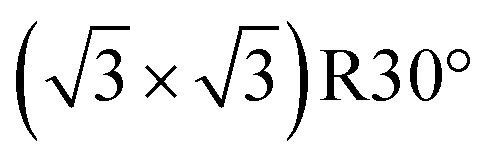 structure.
Phonon dispersion
Several series of time-of-flight (TOF) spectra have been taken under different incident conditions, in order to get the phonon dispersion curves. A representative series of TOF data is shown in Fig. SI2.†Fig. 4 shows the phonon dispersion curves for Gr on sapphire measured along the direction. Phonon dispersion curves for free standing Gr calculated from first principles29 are also shown as dashed lines. No data points were detected for the in-plane longitudinal acoustic (LA) and transverse acoustic (TA) modes. The TA mode is usually forbidden in HAS measurements for planar scattering in the
  direction due to symmetry as has been shown for Gr/Cu(111),20 but this selection rule is not valid in the presence of defects that break the translational symmetry.30 However, the small energy difference between the LA and TA mode makes it very hard to resolve them in the TOF measurements. We therefore could not obtain any information on these two modes here. The out-of-plane acoustic (ZA) mode, on the other hand, is clearly resolved and as expected from the broken symmetry introduced by the sapphire substrate, does not follow a pure acoustic dispersion but has a frequency ω0 = 5.8 meV at the Γ point. The ZA mode exhibits a parabolic dispersion, softened with respect to the one expected for free standing Gr. This softening is related to the presence of point defects in Gr, as shown below.
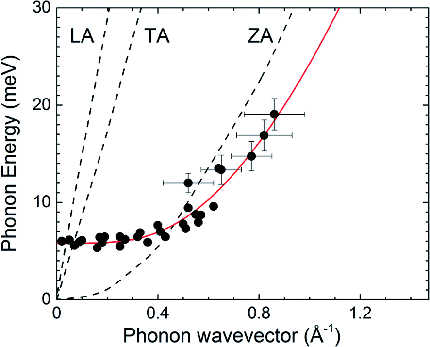 | ||
Fig. 4 Experimentally derived surface phonons for Gr on sapphire measured along the  direction shown with DFT calculations for free standing Gr29 (dashed curves). Error bars are shown for some data points. Red curve is a fit to the data – see text. direction shown with DFT calculations for free standing Gr29 (dashed curves). Error bars are shown for some data points. Red curve is a fit to the data – see text. | ||
The ZA dispersion curve can be used to derive more fundamental quantities like the Gr–sapphire coupling strength, g, and the free standing bending rigidity κ.31 As mentioned above, coupling Gr to a substrate will introduce a gap at a frequency ω0 at the ![[capital Gamma, Greek, macron]](https://www.rsc.org/images/entities/i_char_e0ba.gif) point, and the dispersion relation of the flexural mode ZA is given by:32,33
point, and the dispersion relation of the flexural mode ZA is given by:32,33
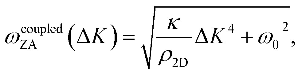 | (1) |
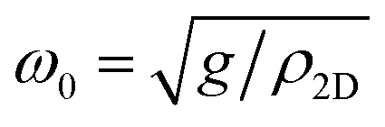 and g is the coupling strength between Gr and substrate.32 Therefore, from a fit to the experimental data using eqn (1) (red curve in Fig. 4) it is possible to determine both g and κ. We obtain g = (5.8 ± 0.4) × 1019 N m−3 for the Gr–sapphire interaction. This value is almost identical to the one reported for Gr–Cu (g = (5.7 ± 0.4) × 1019 N m−3) applying the same procedure.20 However, we get κ = 0.61 ± 0.15 eV for Gr–sapphire, quite below the value reported for Gr–Cu (κ = 1.30 ± 0.15 eV) and for free standing Gr (κ = 1.20–1.61 eV (ref. 31)). This low value of κ reflects the softening of the ZA mode with respect to the one of free standing Gr, and points to a lower Young’s modulus of Gr on sapphire. A recent study has shown that the elastic modulus of Gr decreases with a higher density of vacancies in the Gr lattice.34 Extrapolation of the data presented in ref. 34 shows that a reduction of the Young’s modulus by a factor of 2 can be induced by 2% vacancies. Thus, our results can be interpreted as due to the presence of additional defects in Gr/sapphire (as compared to Gr/Cu), which might arise during the sample preparation through Cu evaporation in vacuum.
AFM results
Atomic force microscopy confirms the presence of Gr domains over lateral scales of microns in the metal-free regions between Cu microislands (0.5–1 μm height, 0.5–5 μm lateral diameter, based on optical and atomic force microscopy scrutiny) formed after Cu evaporation. AFM characterization is focused on the metal-free areas, as shown in Fig. 5. AFM topographic images show the presence of large Gr-covered areas (a substrate coverage ranging 55–80% was estimated from the analysis of several regions of the sample, as illustrated in ESI, Fig. SI3†). Graphene flakes reach 1–3 μm size; actually, it seems that some Gr flakes of approximately 3 μm size suspended on the sapphire substrate are apparently torn into smaller flakes. By comparison of this sample with the one with initial thickness of 500 nm Cu (see Fig. SI4†), we show that the increasing of the thickness leads to a wider Gr coverage. A profile analysis revealed that the Gr layers on the sapphire substrate have a height of 6–8 Å, in agreement with the thickness of monolayer Gr,12 showing randomly oriented wrinkles of 1–4 nm size (see height profiles in Fig. 5a and b). Actually, root mean-square (rms) roughness of the Gr layers averaged from randomly selected flakes is 5.3 Å, visibly rougher than the smooth single crystal sapphire substrate, which exhibits an rms roughness of 2.2 Å. An illustration of the rms roughness study is depicted in the ESI file as Fig. SI5.† Moreover, residual Cu nanometric grains are observed at the boundaries of the Gr domains, presenting an average size of 2–4 nm, as illustrated in the height profiles (Fig. 5a).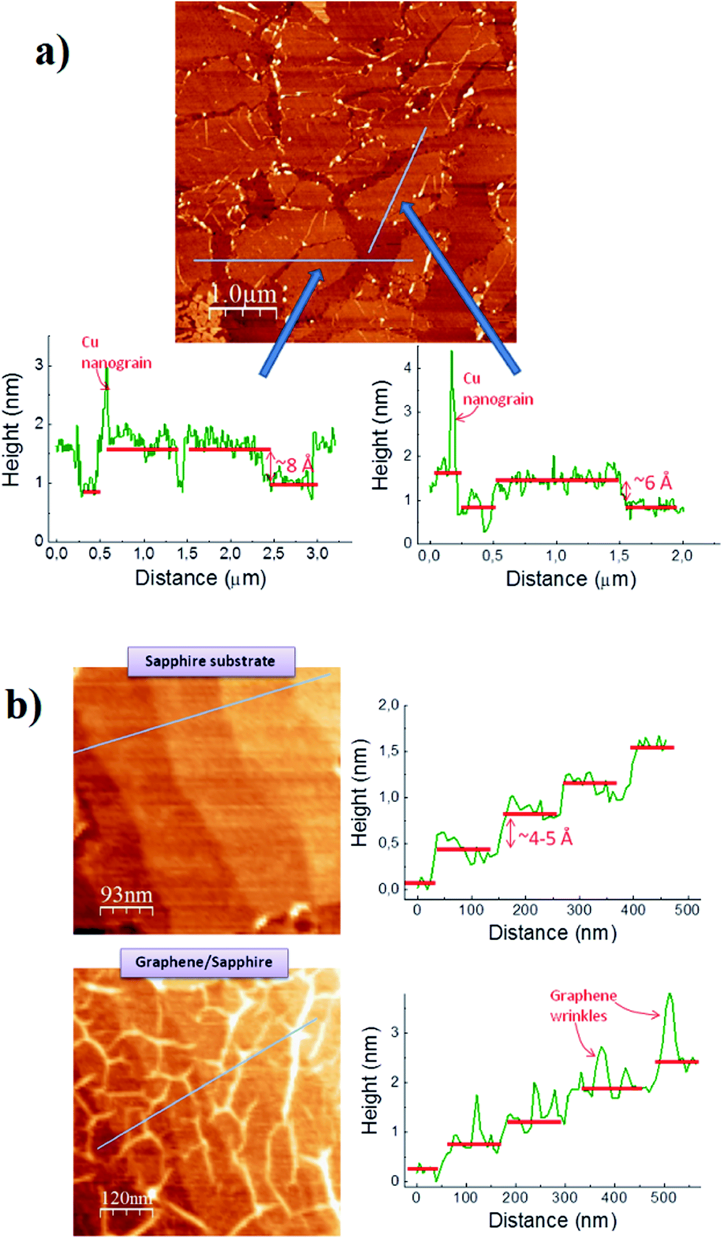 | ||
| Fig. 5 (a) AFM topographic image of the Gr/sapphire sample (image: 5 μm × 5 μm, trying to get an appropriate vision of the Gr flake dimensions). AFM image and height profile analysis reveal discontinuous Gr layers of size up to 3 μm, with ∼6–8 Å height. (b) AFM images of another region showing zoomed areas representative of the sapphire substrate and Gr/sapphire, with respective height profiles, illustrating the presence of steps corresponding to the substrate and how Gr accommodates to the substrate surface. | ||
The substrate reveals a wavy morphology, attributed to the presence of terraces (see Fig. 5b) typical of (0001) single crystal sapphire.10 The height of the steps ranges between 4 and 5 Å (i.e. around c/3, where c = 12.99 Å is the lattice constant of c-plane sapphire), and its periodicity ranges between 100–150 nm. However, an estimation of the coherence length obtained from the width of the specular HAS peak, that gives an average terrace size24 of 40 nm, is smaller than the terrace periodicity measured with AFM. This is consistent with the high sensitivity of HAS to low densities of defects, which leads in average to the detection of smaller terraces. Moreover, the sample exhibits the peculiar morphology of the substrate. From the AFM images in the dynamic mode, the presence of nanometric pits decorating the sapphire substrate is corroborated, predominantly located at the Gr flake boundaries, not present in the bare substrate areas (see Fig. SI6†).
To gain insight into the possible presence of nanometric pits, we have carried out an additional AFM experiment in the contact mode, which in principle would require a lower spring constant (range 0.1–1 N m−1),35,36 using a tip adequate for the dynamic mode with a stronger spring constant (10–100 N m−1). Such a strong spring constant of the tip eventually removed the Gr layers, allowing extra topological information and revealing differences between the bare substrate and the substrate underneath the Gr flakes. Contact mode images (Fig. SI6†) confirm the presence of a pit array originally located at the Gr boundary, likely determining the Gr dimensions (depth 1–2 nm; width variable from 20 to 100 nm). Also, some nanometric pits were observed, to a lesser extent, in the regions where originally Gr settled. The origin of these nanometric pits in the sapphire substrate is likely due to Al2O3 carbothermal reduction in vacuum.10,37 It is suggested that the tearing process of the Gr layer can be attributed to an effect of such substrate carbothermal reduction combined with the breakthrough of the Gr layer by the evaporated copper.
Raman spectroscopy
Optical transmission and Raman micro-spectroscopy were also used to characterize the Gr before and after the elimination of the copper film for a film thickness of 1000 nm Cu. The Raman spectra indicate that single layer graphene is found all over the sample in all cases (Fig. SI7 of the ESI†). AFM measurements indicate that the height of the Gr flakes with respect to the substrate is in the range 6–8 Å, which is consistent with single layer graphene. The optical image in Fig. 6a shows the remaining sparse Cu microislands after Cu evaporation. The optical transmission for a 4 mm diameter area after annealing at 1150 K is around 80% and the characteristic transition at 267 nm reveals the presence of Gr (Fig. 6b). We ascribe the weak feature around 580 nm to the plasmon of remaining Cu microstructures, which can also be seen in the optical (Fig. 6a) and AFM images (Fig. 5a). The quotient of the intensities of the characteristic Gr G and 2D Raman peaks, I2D/IG, is related to the quality of the Gr domains, that is, the regularity of the carbon network. For values close to that of pristine Gr the ratio decrease is related to the presence of strain fields and doping.38,39 At a high concentration of defects which involves breaking a large fraction of the sp2 C![[double bond, length as m-dash]](https://www.rsc.org/images/entities/char_e001.gif) C bonds by the formation of vacancies, irregular rings such as Stone Wales defects or O, OH– or other functional groups, the I2D/IG ratio decreases very significantly and the width of all Raman peaks increases.40 The so-called defects peak D (TO mode close to the
C bonds by the formation of vacancies, irregular rings such as Stone Wales defects or O, OH– or other functional groups, the I2D/IG ratio decreases very significantly and the width of all Raman peaks increases.40 The so-called defects peak D (TO mode close to the ![[K with combining macron]](https://www.rsc.org/images/entities/i_char_004b_0304.gif) point of the Brillouin zone) is activated by the presence of defects that supply the required momentum for the Raman process. Therefore, both I2D/IG and ID/IG ratios are used to evaluate the Gr quality. Graphene in the as deposited samples is of high quality, with a typical I2D/IG ratio for Gr on copper and no defects peak D, as shown in Fig. SI7.† After annealing Gr to 1150 K, the I2D/IG ratio is very similar to the as deposited sample but the defect peak clearly increases (Fig. SI7 from ESI† and Fig. 6g and h). This has been observed for Gr on remaining Cu regions and in areas where Cu has been completely eliminated.
point of the Brillouin zone) is activated by the presence of defects that supply the required momentum for the Raman process. Therefore, both I2D/IG and ID/IG ratios are used to evaluate the Gr quality. Graphene in the as deposited samples is of high quality, with a typical I2D/IG ratio for Gr on copper and no defects peak D, as shown in Fig. SI7.† After annealing Gr to 1150 K, the I2D/IG ratio is very similar to the as deposited sample but the defect peak clearly increases (Fig. SI7 from ESI† and Fig. 6g and h). This has been observed for Gr on remaining Cu regions and in areas where Cu has been completely eliminated.
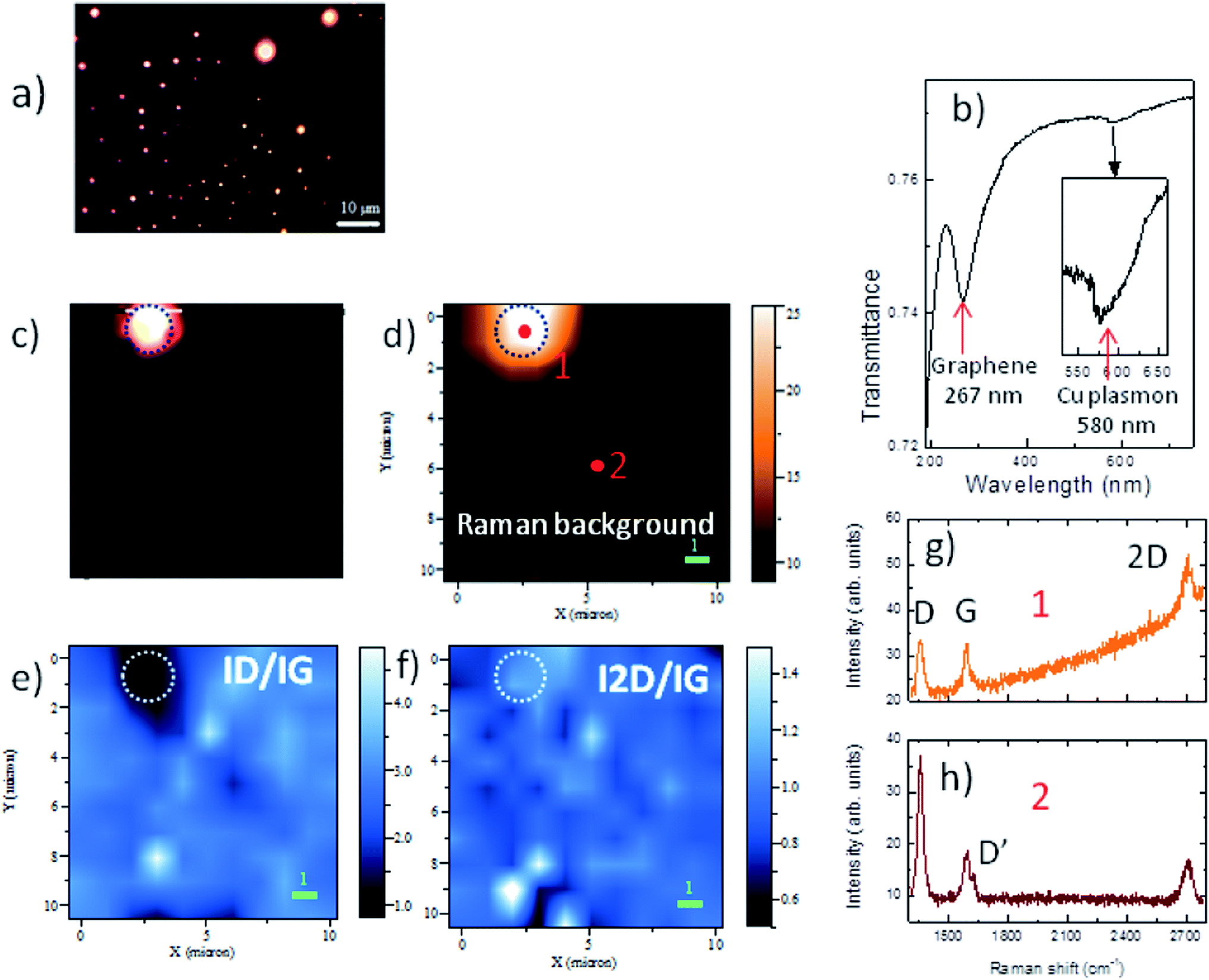 | ||
| Fig. 6 (a) Optical images with Cu residues (scale bar 10 μm). (b) Optical transmittance in a 4 mm diameter area. The interband Gr transition and Cu plasmon (a zoom is shown in the inset) are indicated. (c) Optical image, (d) Raman image (10 × 10 μm2) of the background revealing the Cu residues. (e) ID/IG and (f) I2D/IG Raman images. Raman spectra of Gr on sapphire sample (g) and on Cu (or remaining Cu microstructures) (h). D, G and 2D characteristic peaks of Gr are indicated. | ||
The situation is analogous for Gr deposited on 500 and 1000 nm Cu films. Raman images of Gr/sapphire have been measured to obtain a statistical analysis of the relevant parameters. The optical image of a 10 × 10 μm2 area of the sample is replicated by the Raman image of the background due to Cu (2000–2500 cm−1 region) (Fig. 6c and d) allowing us to distinguish Gr/Cu and Gr/sapphire regions (Fig. 6g and h). This area is representative of the measured Raman images. The image obtained from the I2D/IG intensity ratio (Fig. 6f) evidences the uniformity of Gr over the sample and its quality in terms of the regularity of the carbon network, which is similar to the as-deposited Gr. On the contrary, the ID/IG image indicates that the density of defects on sapphire is higher that on the remaining Cu regions (Fig. 6e). The intensity of the D peak is a compromise between an enhancing factor, the formation of defects that allows the Raman process, and a depleting factor which is the reduction of the density of carbon aromatic rings. The D mode corresponds to a vibration of the aromatic rings while G vibration only requires sp2 hybridization of carbon, therefore G peak intensity is much less sensitive to the presence of defects. The ID/IG ratio is used to estimate the density of point defects (0D defects) or the size of Gr grains (1D defects) by using different formulas. Both situations present similar behavior upon increasing the defect density or reducing the Gr size: the ID/IG ratio first increases up to a maximum value that depends on the excitation wavelength (stage I) and then decreases (stage II). Deciding which kind of defect (0D or 1D) is predominant is not straightforward in most cases. The pioneering work of Tuinstra and Koening (TK)41 on nanocrystalline graphite established that ID/IG = C/La, where La is the graphite crystallite size and C depends on the laser excitation wavelength. This dependence was established to be C(λ) (nm) = 2.4 × 10⁻¹⁰λ4 (nm)42 (stage I) but below around 2–3 nm there is a second regime (stage II) where the ratio decreases as the crystallite size is reduced ID/IG = C′La2.43 The constant C′ is obtained by imposing continuity between both stages resulting in our case C′ ∼ 0.438 for λlaser = 488 nm. On the other hand, the controlled ion bombardment of Gr with different doses to produce carbon vacancies has led to the formulation of a phenomenological model that correlates ID/IG and the distance between the defects, LD.43 The functional dependences of La (black lines) and LD (red circles) versus ID/IG are plotted in Fig. 7a for λlaser = 488 nm.
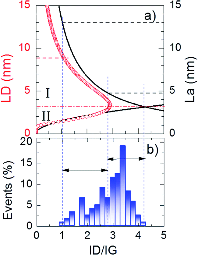 | ||
| Fig. 7 (a) La (black lines) and LD (red circles) versus ID/IG for λlaser = 488 nm; (b) statistical distribution of ID/IG values in the Raman image of Fig. 6e. | ||
Fig. 7b shows the number of events of the ID/IG values obtained in the Raman image of Fig. 6e. The distribution is wide and reaches ID/IG ratio up to 4. Since both La and LD are bivaluated, to know whether Gr is in stage I or II we have to look at the widths of the peaks and at the I2D/IG values. The narrowness of the peaks and the high I2D/IG ratio ensure that Gr is in stage I in spite of the very high ID/IG values. The wide distribution of Fig. 7a can be explained to be due to Gr domains with size LD from 14 to 3 nm (following the black curve in stage I) or to a combination of large regions with point defects with distances LD = 3 to 9 nm (from the curve with red circles) for the lower ID/IG values up to around 2.9 and small Gr domains in the range from 3 to 5 nm for 2.9 < ID/IG < 4. These two scenarios cannot be differentiated by Raman spectroscopy alone; however, the information provided by He diffraction indicates that large coherent domains are present therefore discarding the first case. The 0D defects density can be then calculated for the ID/IG < 2.9 using nD (cm−2) = 1014/πLD2 (ref. 43 and 44) obtaining nD = 3 × 10¹³ to 3 × 1012 cm−2. Since the density of carbon atoms in Gr is 3.9 × 1015 cm−2, the estimated defect fractions, from 0.7% to 7%, are below the threshold for the reduction of He diffraction intensity.
Discussion
An important message from our study is that the wrong conclusion might be drawn if both HAS and Raman results were not available. The observation of clear diffraction peaks, including a moiré pattern, suggests the existence of a well-ordered Gr overlayer, with little presence of defects, whereas the observation of such a pronounced D peak in the Raman spectra points to a Gr layer broken into nanometric patches or grains. It should be kept in mind that the two techniques probe different length-scales and are sensitive to different aspects of Gr. While HAS probes macroscopic regions (mm), Raman microscopy averages information from areas ∼0.7 μm in diameter. Most importantly, the He-diffraction signal originates from the less defective regions while the Raman D peak originates exclusively from the defects of Gr (red areas in Fig. 8). Therefore, these techniques reveal quite different aspects of the same samples. Nevertheless, the high intensity of the HAS diffraction peak indicates its origin from a large fraction of the sample and the hundreds of Raman spectra collected across several 10 μm × 10 μm areas present small variations. Therefore, the combination of both sets of data proves the existence of large domains of Gr with localized defects as carbon vacancies or arrays of vacancies probably originating during the Cu evaporation at the wrinkles or defects present in the initial Gr layer grown on the Cu film.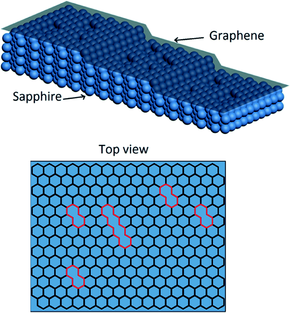 | ||
| Fig. 8 Simplified view of the model proposed to explain both HAS and Raman results of Gr on sapphire. The top view shows a surface area leading to He-diffraction. The red areas represent regions leading to the appearance of Raman D signal (Gr defects). See text for details. | ||
The average domain size of Gr/sapphire derived from HAS is 2000 nm, in good agreement with the Gr size obtained from AFM data. For the underlying sapphire substrate, AFM images show terraces (4–5 Å height) with an average domain size of 120 nm, much larger than the 40 nm obtained for the sapphire substrate from the specular width in HAS (which sets a lower limit to the domain size). The different values obtained with AFM and HAS for the average domain size of sapphire are a consequence of the different interaction mechanisms involved in both techniques. Thermal energy He atoms interact with the surface at a very low electron density (ca. 10−4 a.u.), 2–3 Å above the surface atoms. This interaction is characterized by a large cross section to single defects. Thus, defects on sapphire reduce the domain size as seen by HAS, leading to the detection of smaller terraces on average as compared to AFM. The larger domain size observed for Gr/sapphire is a consequence of a similar mechanism. The Gr layer covers the sapphire substrate like a carpet (see Fig. 8), hiding defects and steps, leading to the appearance of larger coherently diffracting domains. This mechanism can be deduced from the strong reduction of the specular FWHM for Gr/sapphire as compared to the sapphire substrate.
The high sensitivity of HAS to point defects, combined with the Debye–Waller attenuation of diffraction intensities, makes it impossible to detect diffraction from surfaces as soon as the density of defects is larger than 15–20%. This explains for instance the absence of diffraction features from sapphire substrates prepared from scratch, in situ, in our laboratory. Thus, from the observation of high specular reflectivity and diffraction peaks from Gr/sapphire, we can conclude that the density of point defects must be near 5%. This is consistent with the estimation made from the Raman data (0.7 to 7%) and the 2% derived from the determination of the bending rigidity by phonon measurements. The almost complete elimination of Cu is attained without any significant deterioration of the Gr film. This is possible due to the strong planar C–C bond in comparison with the weak Gr–Cu interaction. Presumably, the copper film leaves the substrate through defects and borders of the Gr patches as indicated by the detection of ultra-small Cu particles (around 2–3 nm) at these borders (Fig. 5a).
Conclusions
We have shown that a high-quality Gr layer on sapphire can be grown by heating in UHV a Gr layer prepared by CVD on Cu(111)/Al2O3. The heating process leads to evaporation of the Cu film, leaving a Gr layer deposited on the sapphire substrate. These samples require a short preparation time (30 minutes) and moderate heating temperatures (∼900 °C). Since the method is performed in UHV, it keeps the Gr surface free of contaminants. These samples present a high transparency (80%) in the visible range, making them suitable for many applications. Raman mapping shows that the G to 2D peak ratio is comparable for both Gr/Cu/Al2O3 and Gr/Al2O3 samples, suggesting that the final quality is mainly limited by the quality of the starting Gr layer. HAS and AFM data prove the presence of flat and large Gr domains over lateral scales of microns. He-diffraction data reveal that Gr forms an (11 × 11) moiré pattern, aligned with the (1 × 1) sapphire unit cell. The bending rigidity k = 0.61 ± 0.15 eV and the Gr–sapphire coupling strength g = (5.8 ± 0.4) × 1019 N m−3 have been determined from HAS data of the phonon dispersion of the Gr flexural mode. Our study shows that HAS and Raman provide complementary information on the sample’s quality, and that the wrong conclusion might be drawn if only one of these techniques is applied.Acknowledgements
This project was sponsored by the European Union, Seventh Framework Programme: Theme NMP.2012.1.4-3 Grant no. 309672. AMW and HKY acknowledge support from the Alexander von Humboldt Foundation, the Max Planck EPFL Center for Molecular Nanoscience and Technology as well as the Deutsche Forschungsgemeinschaft under CRC 1073. Additionally, a part of the research has been supported by the Spanish MINECO, under project MAT2012-37276-C03-01, and by Comunidad de Madrid, under project S2013/MIT-2740 (PHAMA_2.0-CM).References
- K. Ellmer, Nat. Photonics, 2012, 6, 809 CrossRef.
- D. Wei and J. Kivioja, Nanoscale, 2013, 5, 10108 RSC.
- F. Bonaccorso, L. Colombo, G. Yu, M. Stoller, V. Tozzini, A. C. Ferrari, R. S. Ruoff and V. Pellegrini, Science, 2015, 347, 1246501 CrossRef PubMed.
- D. Lee, H. Lee, Y. Ahn, Y. Jeong, D.-Y. Leeb and Y. Lee, Nanoscale, 2013, 5, 7750 RSC.
- X. Li, W. Cai, J. An, S. Kim, J. Nah, D. Yang, R. Piner, A. Velamakanni, I. Jung, E. Tutuc, S. K. Banerjee, L. Colombo and R. S. Ruoff, Science, 2009, 324(5932), 1312–1314 CrossRef PubMed.
- Y. Lee, S. Bae, H. Jang, S. Jang, S. E. Zhu, S. H. Sim, Y. I. Song, B. H. Hong and J. H. Ahn, Nano Lett., 2010, 10(2), 490–493 CrossRef PubMed.
- S. Bhaviripudi, X. Jia, M. S. Dresselhaus and J. Kong, Nano Lett., 2010, 10(10), 4128–4133 CrossRef PubMed.
- S. Bae, et al. , Nat. Nanotechnol., 2010, 5, 574–578 CrossRef PubMed.
- H. Ago, Y. Ogawa, M. Tsuji, S. Mizuno and H. Hibino, J. Phys. Chem. Lett., 2012, 3(16), 2228–2236 CrossRef PubMed.
- J. Hwang, M. Kim, D. Campbell, H. a. Alsalman, J. Y. Kwak, S. Shivaraman, A. R. Woll, A. K. Singh, R. G. Hennig, S. Gorantla, M. H. Rümmeli and M. G. Spencer, ACS Nano, 2013, 7, 385–395 CrossRef PubMed.
- M. A. Fanton, J. A. Robinson, C. Puls, Y. Liu, M. J. Hollander, B. E. Weiland, M. LaBella, K. Trumbull, R. Kasarda and C. Howsare, et al. , ACS Nano, 2011, 5, 8062–8069 CrossRef PubMed.
- A. Ismach, C. Druzgalski, S. Penwell, A. Schwartzberg, M. Zheng, A. Javey, J. Bokor and Y. Zhang, Nano Lett., 2010, 10, 1542–1548 CrossRef PubMed.
- H. K. Yu, K. Balasubramanian, K. Kim, J. L. Lee, M. Maiti, C. Ropers, J. Krieg, K. Kern and A. M. Wodtke, ACS Nano, 2014, 8, 8636–8643 CrossRef PubMed.
- D. Farías and K. H. Rieder, Rep. Prog. Phys., 1998, 61, 1575–1664 CrossRef.
- B. Poelsema and G. Comsa, Scattering of Thermal Energy Atoms from Disordered Surfaces, Springer, Berlin, 1989 Search PubMed.
- B. Borca, S. Barja, M. Garnica, M. Minniti, A. Politano, J. M. Rodriguez-García, J. J. Hinarejos, D. Farías, A. L. Vázquez de Parga and R. Miranda, New J. Phys., 2010, 12, 093018 CrossRef.
- A. Politano, B. Borca, M. Minniti, J. J. Hinarejos, A. L. Vázquez de Parga, D. Farías and R. Miranda, Phys. Rev. B: Condens. Matter Mater. Phys., 2011, 84, 23 Search PubMed.
- H. Shichibe, Y. Satake, K. Watanabe, A. Kinjyo, A. Kunihara, Y. Yamada, M. Sasaki, W. W. Hayes and J. R. Manson, Phys. Rev. B: Condens. Matter Mater. Phys., 2015, 91, 155403 CrossRef.
- A. Tamtögl, E. Bahn, J. Zhu, P. Fouquet, J. Ellis and W. Allison, J. Phys. Chem. C, 2015, 119, 25983 Search PubMed.
- A. Al Taleb, H. K. Yu, G. Anemone, D. Farías and A. M. Wodtke, Carbon, 2015, 95, 731–737 CrossRef.
- G. Comsa, Surf. Sci., 1979, 81(1), 56–68 CrossRef.
- W. A. Schlup and K. H. Rieder, Phys. Rev. Lett., 1986, 56, 73 CrossRef PubMed.
- F. Hofmann, J. P. Toennies and J. R. Manson, J. Chem. Phys., 1994, 101, 10155 CrossRef.
- J. Lapujoulade, Y. Lejay and G. Armand, Surf. Sci., 1980, 95, 107–130 CrossRef.
- B. Holst and W. Allison, Nature, 1997, 390, 244 CrossRef.
- K. Fladischer, H. Reingruber, T. Reisinger, V. Mayrhofer, W. E. Ernst, A. E. Ross, D. A. MacLaren, W. Allison, D. Litwin and J. Galas, New J. Phys., 2010, 12, 033018 CrossRef.
- D. Barredo, F. Calleja, P. Nieto, J. J. Hinarejos, G. Laurent, A. L. Vázquez de Parga, D. Farías and R. Miranda, Adv. Mater., 2008, 20, 3492–3497 CrossRef CAS.
- J. B. Nelson and D. P. Riley, Proc. Phys. Soc., 1945, 57, 477 CrossRef CAS.
- J. A. Yan, W. Y. Ruan and M. Y. Chou, Phys. Rev. B: Condens. Matter Mater. Phys., 2008, 77, 125401 CrossRef.
- F. de Juan, A. Politano, G. Chiarello and H. A. Fertig, Carbon, 2015, 85, 225–232 CrossRef CAS.
- Y. Wei, B. Wang, J. Wu, R. Yang and M. L. Dunn, Nano Lett., 2013, 13, 26–30 CrossRef CAS PubMed.
- B. Amorin and F. Guinea, Phys. Rev. B: Condens. Matter Mater. Phys., 2013, 88, 115418 CrossRef.
- A. Al Taleb and D. Farías, J. Phys.: Condens. Matter, 2016, 28, 103005 CrossRef PubMed.
- G. Lopez-Polin, C. Gómez-Navarro, V. Parente, F. Guinea, M.-I. Katsnelson, F. Pérez-Murano and J. Gómez-Herrero, Nat. Phys., 2014, 11, 26–31 CrossRef.
- A. J. Marsden, M. Phillips and N. R. Wilson, Nanotechnology, 2013, 24, 255704 CrossRef CAS PubMed.
- M. Halmann, A. Steinfeld, M. Epstein and I. Vishnevetsky, Miner. Process. Extr. Metall. Rev., 2014, 35, 126–135 CrossRef CAS.
- F. Jiménez-Villacorta, E. Climent-Pascual, R. Ramírez-Jiménez, J. Sánchez-Marcos, C. Prieto and A. de Andrés, Carbon, 2016, 101, 305 CrossRef.
- M. Kalbac, A. Reina-Cecco, H. Farhat, J. Kong, L. Kavan and M. S. Dresselhaus, ACS Nano, 2010, 4, 6055–6063 CrossRef CAS PubMed.
- X. Díez-Betriu, S. Álvarez-García, C. Botas, P. Álvarez, J. Sánchez-Marcos, C. Prieto, R. Menéndez and A. de Andrés, J. Mater. Chem. C, 2013, 1, 6905 RSC.
- F. Tuinstra and J. L. Koenig, J. Chem. Phys., 1970, 53, 1126–1130 CrossRef CAS.
- L. G. Cançado, K. Takai, T. Enoki, M. Endo, Y. a. Kim, H. Mizusaki, A. Jorio, L. N. Coelho, R. Magalhães-Paniago and M. A. Pimenta, Appl. Phys. Lett., 2006, 88, 1–4 CrossRef.
- A. Ferrari and J. Robertson, Phys. Rev. B: Condens. Matter Mater. Phys., 2000, 61, 14095 CrossRef CAS.
- M. M. Lucchese, F. Stavale, E. H. M. Ferreira, C. Vilani, M. V. O. Moutinho, R. B. Capaz, C. A. Achete and A. Jorio, Carbon, 2010, 48, 1592–1597 CrossRef CAS.
- A. C. Ferrari and D. M. Basko, Nat. Nanotechnol., 2013, 8, 235–246 CrossRef CAS PubMed.
Footnote |
| † Electronic supplementary information (ESI) available. See DOI: 10.1039/c5ra27452d |
| This journal is © The Royal Society of Chemistry 2016 |