Comparison of sandwich and fingers-crossing type WO3/BiVO4 multilayer heterojunctions for photoelectrochemical water oxidation†
Cong Liu,
Jinzhan Su* and
Liejin Guo
International Research Centre for Renewable Energy, State Key Laboratory of Multiphase Flow in Power Engineering, Xi’an Jiaotong University, Shaanxi 710049, P. R. China. E-mail: j.su@mail.xjtu.edu.cn
First published on 2nd March 2016
Abstract
WO3 and BiVO4 thin films were spin-coated on FTO in a intersecting way with the WO3 and BiVO4 overlapping only in the center part, resulting in multilayer fingers-crossing thin films (fingers-crossing heterojunction). Samples with only an overlapped area (sandwich heterojunction) were obtained by cutting off the non-overlapped area of both the WO3 and BiVO4 layers (the nodes) as a counterpart for comparison. The influence of layer number, layer thickness and junction type on the photoelectrochemical (PEC) water splitting performance under simulated solar light for the obtained heterojunctions was investigated. XRD, SEM, XPS and UV-vis absorption measurements were conducted to investigate the structural properties and morphology. The photocurrent density of the sandwich heterojunction is higher than that of the fingers-crossing heterojunction at a low applied bias. The IPCE shows that both the fingers-crossing heterojunction and sandwich heterojunction can effectively utilize light up to 510 nm. Mott–Schottky plots show that the sandwich heterojunction has a more negative flat band potential, which is desirable for water splitting, than the fingers-crossing heterojunction. In addition, the mechanism of photogenerated carrier separation for these two heterojunctions was discussed.
1 Introduction
Photoelectrochemical (PEC) water splitting for hydrogen production has been considered as one of the most promising artificial photosynthesis methods1 to utilize solar energy and address critical energy security and environmental sustainability issues.2–5 Although many semiconductor materials such as TiO2, ZnO, Fe2O3, CdS, and SrTiO3 (ref. 6–9) have been reported to be effective for PEC hydrogen production, most of them are limited in their utilization due to serious photocorrosion, high charge carrier recombination, or a large band gap.10 In order to take full advantage of each material’s merits and avoid its weaknesses, many composite semiconductor materials such as Si/Fe2O3,11 TiO2/CdS,12 ZnO/CdS,13 BiVO4/TiO2,14 BiVO4/ZnO,15 and WO3/Fe2O3 (ref. 16) have been designed and tested to address those issues. In a typical semiconductor heterojunction with type II band alignment, photogenerated electron–hole pairs tend to be spatially separated on different sides of the heterojunction, achieving efficient photogenerated electron–hole pair separation.17,18Recently, BiVO4 photoelectrodes have emerged as a popular semiconductor for photoelectrochemical application and have attracted considerable attention.19–24 BiVO4 owing to its band gap of 2.4 eV (monoclinic) is capable of sufficiently absorbing light of the solar spectrum and is stable against photocorrosion in an aqueous electrolyte with a mild pH (between 3 and 11),25–27 but unfortunately its charge carrier recombination rate is relatively high.4,21 In order to improve the charge carrier separation in BiVO4, the method of combining it with other semiconductors with a suitable band gap energy level and good carrier mobility has been adopted. For example, WO3 has a conduction band (CB) level that is more positive than that of BiVO4 and possesses a good carrier mobility.18,28,29 Many types of WO3/BiVO4 heterojunctions have been fabricated in the past five years. For example, Jae Sung Lee et al.30 fabricated flat WO3/BiVO4 heterojunction photoelectrodes on FTO with the BiVO4 layers optimized. Hyeok Park et al.31 fabricated WO3/Mo–BiVO4 heterojunction photoelectrodes by atomic doping. Ligang Xia et al.32 fabricated a BiVO4/WO3/W heterojunction photoanode on a nanoporous WO3 film. Core/shell WO3/BiVO4 nanowire and nanorod photoanodes were fabricated by Zheng et al.33 and Pihosh et al.34 respectively. To further improve the PEC performance of the WO3/BiVO4 heterojunctions, cobalt phosphate (Co-Pi),29,34,35 FeOOH36 and NiOOH36,37 oxygen evolution catalysts (OECs) were deposited on the WO3/BiVO4 heterojunctions using different technologies. The dynamics of the photogenerated charge carriers in WO3/BiVO4 heterojunction photoanodes was also studied by Ivan Grigioni and his co-workers.38 In our previous study,10,39 a nanostructural WO3/BiVO4 heterojunction with efficient carrier separation was realized. It is desirable to further study this efficient heterojunction to maximize the ability of charge separation in the heterojunction.
However, most reported WO3/BiVO4 heterojunction materials contain only a single heterojunction and don’t yet have efficient light absorption or charge transfer. Fatwa F. Abdi et al.40 reported a charge carrier diffusion length of 70 nm for BiVO4. Reducing the thickness of the BiVO4 layers could be a solution, but its light absorbance is insufficient. Using multilayer heterojunctions may enable these deficiencies to be avoided via controlling the layer thickness and layer number.
In this study, we fabricated fingers-crossing and sandwich type multilayer heterojunction photoelectrodes and compared their PEC performance to investigate the junction-type effect on the PEC water oxidation. Although the maximum photocurrent of the films is much less than the recently recorded value for core–shell WO3/BiVO4 nanorods (6.72 mA cm−2 at 1.23VRHE) reported by Pihosh and his co-workers,34 the effect of the heterojunction structure including the layer number and the way of connecting the components on its performance is rarely investigated. So we have discussed the carrier separation in these two types of multilayer heterojunction, and investigated the influence of layer number and layer thickness on the PEC performance. At last, a possible mechanism for the influence of the junction nodes on PEC water splitting was proposed.
2 Experimental
2.1 Film preparation
For the WO3 precursor solution (0.125 M), 0.01 mol tungsten acid (H2WO4) and 25 ml H2O2 (30 wt%) were dissolved in 15 ml de-ionized water (H2O), then mixed with 40 ml of a PVA (poly vinyl alcohol) precursor solution (0.5 g PVA dissolved in 10 ml H2O). For the BiVO4 precursor solution (0.125 M), 0.01 mol Bi(NO3)3·5H2O, 0.01 mol NH4VO3 and 10 ml concentrated nitric acid (HNO3) were dissolved in 30 ml de-ionized water, then mixed with 40 ml PVA solution. Fluorine-doped SnO2 (F:SnO2, FTO)-coated glass substrates (TEC-15, 15 Ω sq−1) were cleaned through successive ultrasonic cleaning with acetone, de-ionized water and ethanol for 30 min, and then dried using a nitrogen flow. An intersecting and overlapping WO3 and BiVO4 structure was synthesized on FTO substrates by the spin-coating of WO3 and BiVO4 layer by layer, the spin rate was controlled at 3000 rpm for 30 s. For the fingers-crossing heterojunction, each layer (any parts undesired for coating were covered with scotch tape) was coated on top of the previous layers after calcination (500 °C/2 h) between the coatings. For the sandwich heterojunction, both the WO3 node and BiVO4 node of the fingers-crossing heterojunction were cut off.2.2 Film characterization
An X’pert PRO diffractormeter (PANalytical, using Cu Ka irradiation, λ = 15.4184 nm) was employed for performing X-ray diffraction (XRD) analysis and determining the structure and phase of the samples. A JSM-7800FE instrument (JEOL) was employed for performing field emission scanning electron microscopy (FE-SEM). X-ray photoelectron spectroscopy (XPS, Axis UltraDLD, Kratos) was used with monochromatic aluminum Kα radiation to obtain the atomic ratio of the samples by etching. Hitachi U-4100 UV-vis-NIR spectrophotometer equipment was used for recording the optical UV-vis absorption spectra of the samples.2.3 Photoelectrochemical measurements
The PEC measurements were performed with a scanning potentiostat (CH Instruments, model CHI 760D) using a standard three-electrode system in 0.5 M Na2SO4 as the electrolyte with Ag/AgCl and a Pt plate as the reference electrode and counter electrode, respectively. The applied bias was converted to a value against a reversible hydrogen electrode (RHE) using eqn (1) below.
 | (1) |
The simulated solar spectrum was generated with a fiber optic spectrometer (AvaSpec-2048) using 350 W xenon lamps set 100 mW cm−2 as the light source. The electrochemical impedance spectroscopy (EIS) was performed at 1.1VRHE with a frequency of 100 kHz–1 Hz under illumination. Apart from the above, a Newport monochromator 74126 and burnt glass made of quartz were used to measure the incident photon to current conversion efficiency (IPCE).
3 Results and discussion
To compare the PEC performances of the sandwich heterojunction and fingers-crossing heterojunction, we prepared bare WO3, fingers-crossing/sandwich WO3–BiVO4-n (n = 1, 2, 3, 4, 5) heterojunctions and bare BiVO4 photoelectrodes via a spin-coating method. The number n denotes the repeat number of the WO3/BiVO4 layers in the fingers-crossing or sandwich heterojunctions. Sandwich heterojunction photoelectrodes were made by cutting off the WO3 node and BiVO4 node areas of the fingers-crossing heterojunction with only the multijunction area left to provide clean cross sections. All the WO3 and BiVO4 layers were prepared using the same conditions. The configurations of the samples are presented in Scheme 1. | ||
| Scheme 1 Geometric illustration of the fingers-crossing heterojunction and sandwich heterojunction. The yellow layer represents BiVO4 and the light blue layer represents WO3. | ||
3.1 Structure and morphology
The crystal structures of the bare film or heterojunctions were examined using XRD analysis. For comparison, the XRD pattern obtained from FTO is also shown in Fig. 1. The XRD patterns of all the photoelectrodes exhibited strong peaks corresponding to FTO of the substrate. The crystal phase of the bare WO3 photoelectrode was identified to be monoclinic (JCPDS card no. 01-071-2141). The bare BiVO4 photoelectrode exhibited a monoclinic scheelite type crystal structure (JCPDS card no. 00-014-0688). For the WO3–BiVO4-n (n = 1, 2, 3, 4, 5) photoelectrodes, the exhibited peaks corresponding to WO3 and BiVO4 indicate the absence of any new compound formation. The X-ray diffraction patterns of WO3–BiVO4-n (n = 2, 4) are shown in Fig. S1.†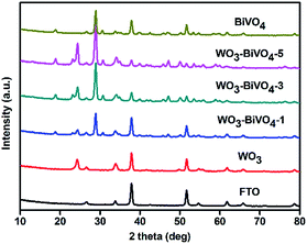 | ||
| Fig. 1 X-ray diffraction patterns of FTO, bare WO3, WO3–BiVO4-n (n = 1, 3, 5) and bare BiVO4 samples. | ||
The surface morphologies of the multilayer heterojunctions are presented in Fig. 2. Bare WO3, bare BiVO4 and WO3–BiVO4-5 show a similar porous morphology but smaller grain sizes compared to that reported by Jae Sung Lee et al.30 This could correspond to the different binder used for spin-coating (PVA in our work and polyethyleneimine (PEI) in Lee’s work). For the bare WO3 film, the porous network with a 50 nm grain size provides a large number of reaction sites and a short distance for holes to travel to the surface.41,42 For the bare BiVO4 film, a larger grain size (∼150 nm) was observed. There is no significant grain size change for the BiVO4 layers in the WO3–BiVO4-5 film as shown in Fig. 2c. The thickness of the WO3–BiVO4-5 film is ca. 324 nm as shown in Fig. 2d. As five cycles of the coating-anneal steps were conducted in the preparation of the WO3–BiVO4-5 film, the thickness of a single WO3/BiVO4 heterojunction was calculated to be ca. 65 nm by dividing 324 nm by 5. All the surface morphologies of the multilayer heterojunctions have little difference since the same synthetic conditions except for the layer number were used.
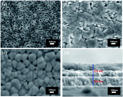 | ||
| Fig. 2 SEM images of the different samples: (a) bare WO3; (b) bare BiVO4; (c) WO3–BiVO4-5; and (d) cross-sectional views of sample WO3–BiVO4-5. | ||
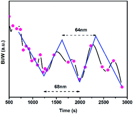
The distribution of the Bi/W atomic ratio as a function of etching time for the multilayer heterojunctions (taking WO3–BiVO4-3(F) as a representative sample) is illustrated in Fig. 3. The etching rate was controlled at 0.1 nm s−1. As the etching time increased, obvious changing of the Bi/W ratio was found along with the different layers, confirming successful fabrication of a multilayer heterojunction. The thickness of a single WO3/BiVO4 bi-layer was determined to be 66 nm by taking the average of 64 nm and 68 nm, which is consistent with the SEM result.
3.2 Optical properties
The optical behavior of the heterojunction photoelectrodes was investigated using UV-vis absorbance spectra as shown in Fig. S2.† The onset of light absorption by the bare WO3 photoelectrode started at 450 nm (Fig. S2a†) in correspondence with its band gap energy of 2.76 eV (Fig. S2b†). The bare BiVO4 photoelectrode exhibited an absorption edge at 500 nm, commensurate with a band gap of 2.56 eV. For the fingers-crossing heterojunction photoelectrodes, the absorption edges were between at 450 nm and 500 nm. All the absorbance intensities increased with increasing layer number while the band absorption edges, which closely resemble the bandgap of BiVO4, were identical. Similar absorbance spectra were observed for the sandwich heterojunction photoelectrodes.3.3 PEC performance of multilayer heterojunction photoelectrodes
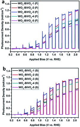
The photocurrent densities were measured using a three electrode system. It was found that the photocurrents of both the fingers-crossing heterojunctions and sandwich heterojunctions (Fig. 4) increased first and then decreased with the layer number increasing. Within the labels for the curves, the number 1 to 5 indicates the layer number of the WO3–BiVO4 bi-layers, F stands for fingers-crossing heterojunction and S stands for sandwich heterojunction. The maximum photocurrent densities for the samples of WO3–BiVO4-3(F) and WO3–BiVO4-3(S) were 1.08 mA cm−2 and 1.05 mA cm−2 at 1.60VRHE, respectively. This can be explained as the number of photogenerated carriers gradually achieved saturation with the increasing layer number while internal recombination started to play a major role when the layer number was higher than 3. At the rising part of the curve, the increase of the layer number lead to higher light absorption and thus a higher photocurrent. While at the decreasing part of the curve, further increase of the layer number increased the distance for charge transport and thus gave a higher recombination rate. A trade-off between the light absorption and the charge transport distance was also reported by Kazuhiro Sayama et al.43Fig. 5a shows the photocurrent densities of the three bi-layers heterojunction photoelectrodes of WO3–BiVO4-3(F) and WO3–BiVO4-3(S). As the applied bias increased, a faster photocurrent density increase was observed for sample WO3–BiVO4-3(S). The photocurrent density of WO3–BiVO4-3(S) was greater than that of WO3–BiVO4-3(F), by approximately 1.1 times at 1.4VRHE. This is ascribed to the presence of nodes which reduced the performance for separation of the photogenerated electron–hole pairs. While with an increased applied bias, currents close to the saturation photocurrent were obtained for both samples. This could be ascribed to the larger applied bias promoting charge carrier separation20 and the influence of WO3 and BiVO4 nodes on the photocurrent was reduced.
In order to compare the photoactive wavelength region for the various photoelectrodes and make a quantitative correlation between the fingers-crossing heterojunction and sandwich heterojunction, incident photon conversion efficiency measurements were conducted under 1.4VRHE in a 0.5 M Na2SO4 aqueous solution. The IPCE can be expressed as:37
 | (2) |
To gain better insight into the efficient water oxidation, charge separation efficiency (ηseparation) and injection efficiency (ηinjection) tests were conducted in a 0.5 M Na2SO4 electrolyte containing 0.5 M H2O2. ηseparation or ηinjection is the fraction of photogenerated holes that does not recombine with electrons in the bulk or at surface traps, respectively. The relationship between the water splitting photocurrent (JH2O), photon absorption photocurrent density (Jabsorbed), ηseparation and ηinjection can be expressed as follows:44,45
| JH2O = Jabsorbed × ηseparation × ηinjection | (3) |
Having H2O2 as a hole scavenger in the electrolyte means that the ηinjection becomes 100% (ηinjection = 1). So, the photocurrent measured with H2O2 in the electrolyte (JH2O2) can be expressed as follows:
| JH2O2 = Jabsorbed × ηseparation | (4) |
Hence, the ηseparation and ηinjection are obtained by dividing JH2O2 by Jabsorbed and dividing JH2O by JH2O2, respectively. The details can be expressed as follows:
| ηseparation = JH2O2/Jabsorbed | (5) |
| ηinjection = JH2O/JH2O2 | (6) |
By measuring the light absorption of the sample WO3–BiVO4-3 and integrating it with respect to the AM 1.5G solar spectrum, Jabsorbed was calculated to be 6.17 mA cm−2. Fig. 5c and d present the charge separation efficiency and injection efficiency, respectively. WO3–BiVO4-3(F) and WO3–BiVO4-3(S) show the same ηseparation as the applied bias increases, which indicates that the nodes show no effect on the recombination between electrons and holes in the bulk. While the obtained different ηinjection values for WO3–BiVO4-3(F) and WO3–BiVO4-3(S) suggests that the nodes influences the recombination behaviour at the surface. At a low applied bias of 0.6VRHE, values of 7.6% and 45.7% were obtained for the WO3–BiVO4-3(F) and WO3–BiVO4-3(S) respectively. However, at a high bias of 1.85VRHE, the same ηinjection (97.2%) was achieved for both the films. These results can be explained as the sandwich type structure of the WO3/BiVO4 multi-layer heterojunction possesses a better surface reaction activity, while for the fingers-crossing structure, a higher applied bias is required to achieve an efficient surface reaction.
Fig. 6 shows the relationship of the layer number with the photocurrent difference value (DV) between samples WO3–BiVO4-n(F) and samples WO3–BiVO4-n(S) at 1.1VRHE. The photocurrent difference is the value obtained by deducting from the photocurrent of the sandwich samples that of the fingers-crossing samples at 1.1VRHE. With the increasing layer number, the photocurrent difference increased first then decreased and reached its maximum value of 0.322 mA cm−2 at three bi-layers. When the layer number is below 3, the photogenerated holes are easily transferred to the electrode/electrolyte interface to oxidize water as the carrier diffusion length of BiVO4 is ca. 70 nm.40 When the layer number is over 3, the large thickness of the films inhibits the hole transfer and reduces the photocurrent.
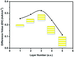 | ||
| Fig. 6 The relationship of the layer number and the photocurrent difference value (DV) between samples WO3–BiVO4-n(F) and WO3–BiVO4-n(S) at 1.1VRHE. | ||
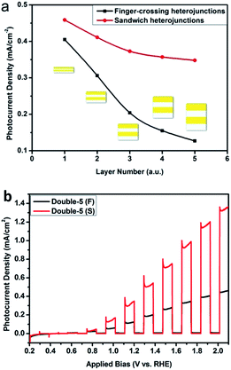
In order to investigate the influence of the thickness of each layer on the photocurrent density, we kept the bi-layer number of the heterojunctions at two and adjusted the thickness of each layer by changing the spin-coating circle number for each layer. The thickness of all the layers was controlled simultaneously by using the same spin-coating circle number. The samples were labelled as double-n (n = 1, 2, 3, 4, 5, n indicates the spin-coating circle number). Fig. 7a shows the photocurrent density of the fingers-crossing heterojunction (double-n (F)) and sandwich heterojunction (double-n (S)) at an applied bias of 1.2VRHE. As the layer thickness increased, the photocurrent densities for both structures decreased. This can be interpreted as due to enhancement of the recombination with the increasing thickness of each layer. The photocurrent density decay with the increase of the thickness of each layer for the sandwich heterojunction is slower when compared to that of the fingers-crossing heterojunction. 76% of the photocurrent (at 1.2VRHE) remained for the sandwich heterojunction while only 31% of photocurrent was left for the fingers-crossing heterojunction. This can be due to a higher recombination rate of the photogenerated electron–hole pairs with the presence of the nodes in the fingers-crossing heterojunction. These results mean that a smaller thickness of each layer could reduce the effects of the nodes. When the concentration of the precursors was reduced to half (0.0625 M), the BiVO4 layer could not cover all of the FTO substrate (Fig. S3†). Thus, the optimum thickness for each layer was controlled by using one spin-coating cycle and a thickness of a single WO3/BiVO4 heterojunction of ca. 65 nm was obtained. It was found that the photocurrent performance of all the fingers-crossing heterojunctions is worse than that of a sandwich heterojunction with the same layer number and thickness. Fig. 7b shows the photocurrents of the fingers-crossing heterojunction and sandwich heterojunction of double-5. The photocurrent density of the double-5 (S) is 2.8 times that of double-5 (F) at 1.6VRHE.
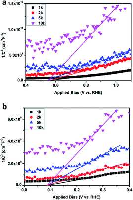
In order to study the effects of WO3 nodes and BiVO4 nodes on the flat band potential, impedance measurements were conducted at different frequencies (1, 2, 5, 10 kHz) on prepared samples in a 0.5 M Na2SO4 electrolyte in the dark and this allowed the construction of Mott–Schottky plots based on the following eqn (7):30
 | (7) |
The x intercept and the slope of the linear region in a plot of Csc−2 versus E are usually used to determine the flat band potential and the density of carriers. A plot of impedance versus frequency (Fig. S4†) was plotted to check the validity of the Mott–Schottky results. As shown in Fig. 8, the flat band potential values of WO3–BiVO4-5(F) and WO3–BiVO4-5(S) were determined to be 0.55VRHE and 0.08VRHE, respectively, and both values are between those of pure WO3 and BiVO4 (1.14VRHE and 0.01VRHE, respectively) and are similar to reported results.30,46 It can be found that the existence of nodes has effects on the flat band potential and the density of carriers. The sandwich heterojunction possesses a more negative flat band potential than the fingers-crossing heterojunction. From the slope, it was found that all the deposited films possess the nature of an n-type semiconductor. For n-type semiconductors, a smaller slope value of WO3–BiVO4-5(S) than that of WO3–BiVO4-5(F) indicates that WO3–BiVO4-5(S) has a larger density of carriers compared to the latter.
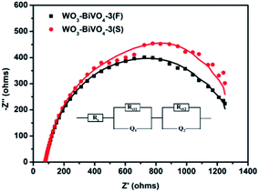
Electrochemical impedance spectroscopy (EIS) was also carried out under front illumination at 1.1VRHE to further compare the charge transfer properties of the fingers-crossing and sandwich heterojunctions. The Nyquist plots of the EIS results are shown in Fig. 9. The circular dots in the plots represent the experimental data, and the solid lines represent the curve fitting using the equivalent circuit model shown inside the plots. In the equivalent Randle circuit, Rs is the solution resistance, Q1 and Q2 are the constant phase elements (CPE) which stand for the electrolyte–photoelectrode interface and the WO3–BiVO4 interface. The Rct1 and Rct2 are the charge transfer resistances across the interfaces of electrolyte–photoelectrode and WO3–BiVO4. The parameters extracted from the equivalent circuit fitting are shown in Table 1. The semicircle at the high frequency end in the Nyquist plot corresponds to the charge transfer resistance (Rct).4,47 As can be seen in Table 1, the sandwich heterojunction WO3–BiVO4-3(S) shows a smaller Rct2 and Q2 than WO3–BiVO4-3(F), presumably resulting from the absence of WO3 nodes and BiVO4 nodes. The smaller Rct2 and Q2 of WO3–BiVO4-3(S) than for WO3–BiVO4-3(F) indicate that the sandwich heterojunction is a structure more favourable for charge transfer than the fingers-crossing heterojunction. While the extracted parameters of Rct1 and Q1 for the fingers-crossing and sandwich heterojunctions are close, indicating that both the WO3 node and BiVO4 node have little effect on the electron transport at the interface of the semiconductor/electrolyte.
| Samples | Rs (Ω) | Rct1 (kΩ) | Q1 | Rct2 (kΩ) | Q2 | ||
|---|---|---|---|---|---|---|---|
| Y01 (10−5) | n1 | Y02 (10−5) | n2 | ||||
| WO3–BiVO4-3(F) | 78.19 | 1.01 | 6.68 | 0.80 | 3.03 | 2.68 | 0.89 |
| WO3–BiVO4-3(S) | 80.12 | 1.32 | 5.36 | 0.74 | 0.19 | 1.89 | 1.00 |
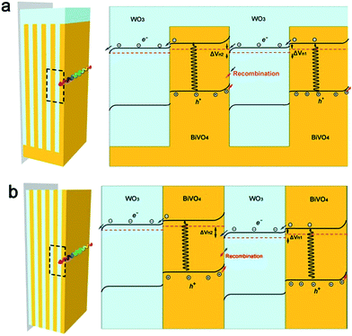
For a WO3–BiVO4 heterojunction in Na2SO4 solution the energy band positions of BiVO4 (VCB = 0.02 eV, VVB = 2.53 eV, V vs. NHE) and WO3 (VCB = 0.41 eV, VVB = 2.77 eV, V vs. NHE) have been reported by Lee.30 It is widely accepted that the bottoms of the conduction bands in several n-type semiconductors are more negative by 0.1 V–0.3 V than the flat band potential.37,48 Based on the band positions, the optical band gap energies and the experimental results discussed above, we proposed a band structure model for our two different types of multilayer heterojunctions as shown in Scheme 2. We take BiVO4/WO3/BiVO4 as one cycle junction and discuss the band structures of each outermost cycle junction (shown in Scheme 2a and b). Both the conduction band and valence band edge of BiVO4 are more negative than the corresponding band edges of WO3. This band structure facilitates the injection of photogenerated electrodes from the conduction band of BiVO4 to that of WO3. For heterojunctions under light irradiation, symmetrical space charge fields En1 and En2 should generate two voltages (ΔVn1 and ΔVn2) in opposite directions.49 For the fingers-crossing heterojunction, the WO3 node connects all the WO3 fingers resulting in an equipotential within all the WO3 layers. The same situation should be expected for all the BiVO4 layers. These equipotential connections contribute to the same amplitude of ΔVn1 and ΔVn2. This indicates that the total voltage difference (ΔVn) in one cycle junction should be zero (ΔVn1 + ΔVn2 = 0) at the adjacent junctions. However, underlying junctions will generate a smaller photovoltage (ΔVn) as less light is absorbed. The case for the sandwich heterojunctions without WO3 or BiVO4 nodes is different. With the absence of an equipotential connection, there is an additional Fermi level drop in the outer BiVO4 layer induced by electrons flowing to the double layer across the BiVO4/electrolyte. Thus, the space charge region at BiVO4/WO3 was strengthened while that at WO3/BiVO4 was weakened, resulting in ΔVn1 < ΔVn2. As for the next BiVO4/WO3/BiVO4 cycle, the space charge region of WO3/BiVO4 was weakened because that of BiVO4/WO3 in the previous cycle was strengthened. With repetition of the BiVO4/WO3/BiVO4 cycles, the conduction band edges of the semiconductors for each layer in the sandwich heterojunction gradually shifted to negative values, as shown in Scheme 2b. That is why the flat-band potential of the sandwich heterojunction is more negative compared to that of the fingers-crossing heterojunction, and this flat-band potential shift is beneficial for charge separation and thus the photoelectrochemical activity.
4 Conclusions
Fingers-crossing heterojunction and sandwich heterojunction WO3/BiVO4 photoelectrodes were fabricated on FTO substrates. Both the as-prepared WO3 layer and BiVO4 layer possess a monoclinic phase. The influence of layer number and layer thickness on the PEC performance was investigated, and the optimal layer number was found to be 3 layers and the best thickness for each layer was the thinnest thickness used. It was also found that the flat band potential for the sandwich heterojunction shifted to be more negative compared to the fingers-crossing one and an enhancement of the PEC performance for hydrogen production was observed especially when applied with a low bias. This work compared two different types of heterojunctions and showed that the PEC properties are sensitive to the junction type. With regard to further improvement of the PEC performance of heterojunctions, optimizing the structure of the electrode remains a promising approach, and it can also inspire ideas for investigating other heterostructures.Acknowledgements
This work was supported by the National Natural Science Foundation of China (No. 51202186).Notes and references
- H. W. Jeong, T. H. Jeon, J. S. Jang, W. Choi and H. Park, J. Phys. Chem. C, 2013, 117, 9104–9112 CAS.
- K. Zhang and L. Guo, Catal. Sci. Technol., 2013, 3, 1672 CAS.
- D. Eisenberg, H. S. Ahn and A. J. Bard, J. Am. Chem. Soc., 2014, 136, 14011–14014 CrossRef CAS PubMed.
- X. Fu, M. Xie, P. Luan and L. Jing, ACS Appl. Mater. Interfaces, 2014, 6, 18550–18557 CAS.
- P. Chatchai, A. Y. Nosaka and Y. Nosaka, Electrochim. Acta, 2013, 94, 314–319 CrossRef CAS.
- F. E. Osterloh, Chem. Soc. Rev., 2013, 42, 2294–2320 RSC.
- R. Daghrir, P. Drogui and D. Robert, Ind. Eng. Chem. Res., 2013, 52, 3581–3599 CAS.
- K. Sivula, F. L. Formal and M. Grätzel, ChemSusChem, 2011, 4, 432–449 CrossRef CAS PubMed.
- T. Hisatomi, J. Kubota and K. Domen, Chem. Soc. Rev., 2014, 43, 7520–7535 RSC.
- J. Su, L. Guo, N. Bao and C. A. Grimes, Nano Lett., 2011, 11, 1928–1933 CrossRef CAS PubMed.
- M. T. Mayer, C. Du and D. Wang, J. Am. Chem. Soc., 2012, 134, 12406–12409 CrossRef CAS PubMed.
- S. Liu, N. Zhang, Z. Tang and Y. Xu, ACS Appl. Mater. Interfaces, 2012, 4, 6378–6385 CAS.
- Y. Tak, S. J. Hong, J. S. Lee and K. Yong, J. Mater. Chem., 2009, 19, 5945 RSC.
- S. Ho-Kimura, S. J. A. Moniz, A. D. Handoko and J. Tang, J. Mater. Chem. A, 2014, 2, 3948 CAS.
- S. J. A. Moniz, J. Zhu and J. Tang, Adv. Energy Mater., 2014, 4, 1301590 Search PubMed.
- K. Sivula, F. L. Formal and M. Grätzel, Chem. Mater., 2009, 21, 2862–2867 CrossRef CAS.
- S. Shenawi-Khalil, V. Uvarov, S. Fronton, I. Popov and Y. Sasson, J. Phys. Chem. C, 2012, 116, 11004–11012 CAS.
- R. Saito, Y. Miseki and K. Sayama, Chem. Commun., 2012, 48, 3833–3835 RSC.
- H. Yoon, M. G. Mali, J. Y. Choi, M.-w. Kim, S. K. Choi, H. Park, S. S. Al-Deyab, M. T. Swihart, A. L. Yarin and S. S. Yoon, Langmuir, 2015, 31, 3727–3737 CrossRef CAS PubMed.
- M. Long, W. Cai and H. Kisch, J. Phys. Chem. C, 2008, 112, 548–554 CAS.
- Y. H. Ng, A. Iwase, A. Kudo and R. Amal, J. Phys. Chem. Lett., 2010, 1, 2607 CrossRef CAS.
- R. Saito, Y. Miseki and K. Sayama, J. Photochem. Photobiol., A, 2013, 258, 51–60 CrossRef CAS.
- Y. Park, K. J. McDonald and K. S. Choi, Chem. Soc. Rev., 2013, 42, 2321–2337 RSC.
- M. Zhong, T. Hisatomi, Y. Kuang, J. Zhao, M. Liu, A. Iwase, Q. Jia, H. Nishiyama, T. Minegishi, M. Nakabayashi, N. Shibata, R. Niishiro, C. Katayama, H. Shibano, M. Katayama, A. Kudo, T. Yamada and K. Domen, J. Am. Chem. Soc., 2015, 137, 5053–5060 CrossRef CAS PubMed.
- S. K. Cho, H. S. Park, H. C. Lee, K. M. Nam and A. J. Bard, J. Phys. Chem. C, 2013, 117, 23048–23056 CAS.
- N. F. Fatwa, F. Abdi, A. Dabirian and R. van de Krol, Mater. Res. Soc. Symp. Proc., 2012, 1446, 7–12 Search PubMed.
- M. T. McDowell, M. F. Lichterman, J. M. Spurgeon, S. Hu, I. D. Sharp, B. S. Brunschwig and N. S. Lewis, J. Phys. Chem. C, 2014, 118, 19618–19624 CAS.
- C. A. Bignozzi, S. Caramori, V. Cristino, R. Argazzi, L. Meda and A. Tacca, Chem. Soc. Rev., 2013, 42, 2228–2246 RSC.
- S. K. Pilli, R. Janarthanan, T. G. Deutsch, T. E. Furtak, L. D. Brown, J. A. Turner and A. M. Herring, Phys. Chem. Chem. Phys., 2013, 15, 14723–14728 RSC.
- S. J. Hong, S. Lee, J. S. Jang and J. S. Lee, Energy Environ. Sci., 2011, 4, 1781–1787 CAS.
- K. Zhang, X. J. Shi, J. K. Kim and J. H. Park, Phys. Chem. Chem. Phys., 2012, 14, 11119–11124 RSC.
- L. Xia, J. Bai, J. Li, Q. Zeng, X. Li and B. Zhou, Appl. Catal., B, 2016, 183, 224–230 CrossRef CAS.
- P. M. Rao, L. Cai, C. Liu, I. S. Cho, C. H. Lee, J. M. Weisse, P. Yang and X. Zheng, Nano Lett., 2014, 14, 1099–1105 CrossRef CAS PubMed.
- Y. Pihosh, I. Turkevych, K. Mawatari, J. Uemura, Y. Kazoe, S. Kosar, K. Makita, T. Sugaya, T. Matsui, D. Fujita, M. Tosa, M. Kondo and T. Kitamori, Sci. Rep., 2015, 5, 11141 CrossRef PubMed.
- Y. Pihosh, I. Turkevych, K. Mawatari, T. Asai, T. Hisatomi, J. Uemura, M. Tosa, K. Shimamura, J. Kubota, K. Domen and T. Kitamori, Small, 2014, 10, 3692–3699 CrossRef CAS PubMed.
- X. Shi, I. Y. Choi, K. Zhang, J. Kwon, D. Y. Kim, J. K. Lee, S. H. Oh, J. K. Kim and J. H. Park, Nat. Commun., 2014, 5, 4775 CrossRef CAS PubMed.
- T. W. Kim and K. S. Choi, Science, 2014, 343, 990–994 CrossRef CAS PubMed.
- I. Grigioni, K. G. Stamplecoskie, E. Selli and P. V. Kamat, J. Phys. Chem. C, 2015, 119, 20792–20800 CAS.
- J. Su, X. Feng, J. D. Sloppy, L. Guo and C. A. Grimes, Nano Lett., 2011, 11, 203–208 CrossRef CAS PubMed.
- F. F. Abdi, T. J. Savenije, M. M. May, B. Dam and R. van de Krol, J. Phys. Chem. Lett., 2013, 4, 2752–2757 CrossRef CAS.
- S. J. Hong, H. C. Jun, P. H. Borse and J. S. Lee, Int. J. Hydrogen Energy, 2009, 34, 3234 CrossRef CAS.
- M. U. Clara Santato and J. Augustynski, J. Phys. Chem. B, 2001, 105, 936–940 CrossRef.
- I. Fujimoto, N. Wang, R. Saito, Y. Miseki, T. Gunji and K. Sayama, Int. J. Hydrogen Energy, 2014, 39, 2454–2461 CrossRef CAS.
- H. Dotan, K. Sivula, M. Grätzel, A. Rothschild and S. C. Warren, Energy Environ. Sci., 2011, 4, 958–964 CAS.
- J. H. Kim, Y. J. Jang, J. H. Kim, J. W. Jang, S. H. Choi and J. S. Lee, Nanoscale, 2015, 7, 19144–19151 RSC.
- M. Li, L. Zhao and L. Guo, Int. J. Hydrogen Energy, 2010, 35, 7127–7133 CrossRef CAS.
- L. Zhang, E. Reisner and J. J. Baumberg, Energy Environ. Sci., 2014, 7, 1402–1408 CAS.
- P. Bornoz, F. F. Abdi, S. D. Tilley, B. Dam, R. van de Krol, M. Graetzel and K. Sivula, J. Phys. Chem. C, 2014, 118, 16959–16966 CAS.
- J. Cao, J. Xing, Y. Zhang, H. Tong, Y. Bi, T. Kako, M. Takeguchi and J. Ye, Langmuir, 2013, 29, 3116–3124 CrossRef CAS PubMed.
Footnote |
| † Electronic supplementary information (ESI) available: XRD of multilayer heterojunctions (Fig. S1), optical behavior of heterojunctions (Fig. S2), SEM image of BiVO4 (Fig. S3), and the dependence of impedance on frequency (Fig. S4). See DOI: 10.1039/c5ra25601a |
| This journal is © The Royal Society of Chemistry 2016 |

