DOI:
10.1039/C6NR06316K
(Paper)
Nanoscale, 2016,
8, 17928-17939
Ultra-thin graphene–polymer heterostructure membranes†
Received
9th August 2016
, Accepted 2nd September 2016
First published on 5th September 2016
Abstract
The fabrication of arrays of ultra-thin conductive membranes remains a major challenge in realising large-scale micro/nano-electromechanical systems (MEMS/NEMS), since processing-stress and stiction issues limit the precision and yield in assembling suspended structures. We present the fabrication and mechanical characterisation of a suspended graphene–polymer heterostructure membrane that aims to tackle the prevailing challenge of constructing high yield membranes with minimal compromise to the mechanical properties of graphene. The fabrication method enables suspended membrane structures that can be multiplexed over wafer-scales with 100% yield. We apply a micro-blister inflation technique to measure the in-plane elastic modulus of pure graphene and of heterostructure membranes with a thickness of 18 nm to 235 nm, which ranges from the 2-dimensional (2d) modulus of bare graphene at 173 ± 55 N m−1 to the bulk elastic modulus of the polymer (Parylene-C) as 3.6 ± 0.5 GPa as a function of film thickness. Different ratios of graphene to polymer thickness yield different deflection mechanisms and adhesion and delamination effects which are consistent with the transition from a membrane to a plate model. This system reveals the ability to precisely tune the mechanical properties of ultra-thin conductive membranes according to their applications.
1. Introduction
Single-layer chemical vapour deposited (CVD) graphene has shown great promise in enabling micro- and nano-electromechanical systems (MEMS and NEMS) that can outperform current polymer and silicon-based state of the art systems.1,2 Its mechanical properties have been proven to match those of its pristine crystalline form whilst allowing for remarkably versatile processability;3 it can be grown over large areas,4 transferred onto arbitrary substrates and patterned by standard photolithography techniques.5,6 Moreover, graphene, even in its polycrystalline CVD form, is impermeable to all gases making it an ideal barrier for high pressure applications.6 Current methods in forming single-layer graphene NEMS devices result in low yields due to capillary effects acting on the suspended material during the graphene transfer process.7,8 In addition, the suspended membranes that survive often suffer from a distorted topography due to a residual transfer polymer on the surface of graphene. This residue limits the in-plane span of membranes and results in poor fabrication yield.9 As well as showing excellent performance characteristics, single-layer graphene devices typically have a footprint of a few microns and therefore allow for aggressive upscaling to achieve improved performance characteristics.1 Although this upscaling has been demonstrated in recent reports on pressure sensing devices, many of the graphene membranes are fractured and there is limited evidence as to how many membranes are actively deflecting;6,10,11 whilst scanning electron microscopy (SEM) can indicate the quantity of membranes that are freely suspended, little information is provided on the existence of nano-scale cracks that allow gas to permeate across the membrane.12 In order to overcome the above mentioned issues of low yield, inhomogeneity and gas permeability, we propose a laminate heterostructure comprising a graphene layer and an ultra-thin polymer layer with excellent structural integrity in the freestanding graphene whilst having a minimal effect on the mechanical and electrical performance of bare graphene.
The stress–strain behaviour of single-layer graphene and graphene–polymer composites has been studied primarily using Raman spectroscopy.13–15 By monitoring the G and 2D peak position and intensities as a function of applied force on a suspended graphene membrane, the strain and deflection of the membrane can be determined.16,17 However, this technique provides indirect measurement of the stress–strain behaviour and probes only a specific area of the membrane, defined by the laser spot size.18 In order to probe the entirety of a mechanical component, a direct micromechanical measurement of the membrane's stress–strain response is required. Micro-blister inflation, in which the deflection of a pressurised suspended membrane is monitored, has been used to study the interfacial and elastic properties of graphene as well as ultra-thin polymers.18–21 An important aspect of the micro-blister inflation technique is that it removes complications due to contact mechanics that arise when large localised forces are applied, such as during nanoindentation.19,22,23
In this study, we perform micro-blister inflation experiments to deduce the in-plane modulus of graphene–polymer heterostructure membranes of thicknesses varying from 18 nm to 235 nm. We show that this system can behave according to the linear plate as well as a non-linear membrane model. Moreover, we measure the sheet resistance of the membranes to confirm their suitability for electromechanical applications. Finally, we use the micro-blister inflation technique to determine the yield of membranes of varying diameter as an indication of the degree of mechanical stability provided by the heterostructure.
2. Results and discussion
2.1 Micro-blister characterisation
Graphene–polymer membranes were fabricated by transferring a graphene–polymer stack onto a patterned Si/SiO2 chip using a poly(methyl methacrylate) (PMMA) polymer support as shown in the schematics in Fig. 1a. In order to examine the membrane morphology at equilibrium and under varying pressure load, we pressurised the micro-cavities enclosed by the membranes using an inflation procedure as shown in Fig. 1b.6 Further details on the fabrication and characterisation procedure are given in the methods section. Successfully transferred samples were inserted into a pressure chamber, pumped with N2 gas to the desired pressure and then left for 24 hours in order for the N2 gas to diffuse into the micro-cavities, equilibrating the pressure across the membrane. On removal of the samples, membranes form a blister above the micro-cavity due to the imbalance in pressure between the lab atmosphere and the micro-cavity. The gas leakage out of the micro-cavity is on the order of several hours allowing sufficient time to conduct atomic force microscopy (AFM) and Raman spectroscopy measurements on the deflected membranes. Depending on the thickness of the heterostructure membranes, blisters took between 2 and 18 hours to deflate to within 10% of their zero deflection point (ESI Fig. S1†).
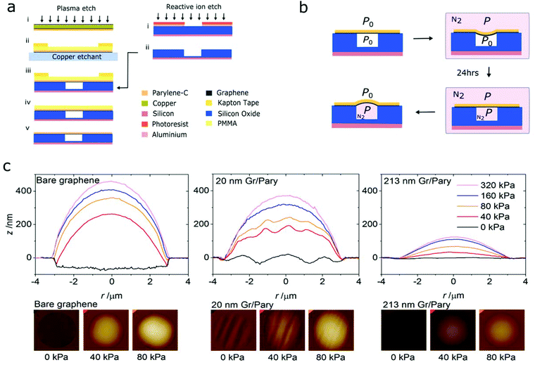 |
| | Fig. 1 (a) Schematic of the fabrication process for suspended graphene–polymer heterostructure membranes. (b) Schematic of the micro-blister inflation procedure of graphene–polymer heterostructure membranes. (c) Cross-section profiles of bare graphene and graphene–polymer heterostructure membranes of thickness 21 nm and 213 nm respectively at various pressures. The 2d AFM height maps below the cross-sections show the respective membranes at 0 kPa, 40 kPa and 80 kPa. | |
This method of probing the mechanical properties of membranes has several advantages over other commonly used methods such as nanoindentation or optical interferometry. First, the non-contact approach prevents any unwanted distortion of the membrane due to tip–surface interactions which may result in non-uniform stresses across the membrane.20 Second, the ScanAsyst™ AFM imaging mode allows us to quickly scan large areas with lateral and height resolutions of approximately 10 nm and 1 nm respectively.22 In addition, by mapping the entire profile of the membrane, we avoid misinterpretations of the maximum deflection point due to contaminants or anomalous wrinkles. Third, pressure is applied uniformly, allowing the use of simple geometric models to determine the stress–strain behaviour of the membrane.23 Fourth, the strong adhesion between the graphene layer and the substrate, combined with the gas impermeability of graphene, gives a stable pressure inside the micro-cavity. This allows us to monitor the gas leakage in order to accurately determine the pressure at the time of measurement.24 Moreover, samples are not confined to a fixed pressure supply, allowing us to freely move pressurised samples between different measurement equipment. For example, micro-blister cross-sections obtained by AFM can be compared with the strain measurements by Raman spectroscopy in order to confirm strain transfer between graphene and polymer layers at a given pressure. Fifth, measurements of statically deflected membranes at room temperature ensure that the transient effects of the viscoelastic Parylene-C layer do not influence the deformation behaviour.25
The equilibrium-pressure cross-section profiles of single-layer CVD graphene (from here on referred to as bare graphene) and graphene–polymer membranes of various thicknesses are shown in Fig. 1c. We note that all pressure values quoted in this report are in reference to atmospheric pressure P0. Bare graphene membranes show a relatively flat profile with minor out-of-plane rippling with amplitude and wavelength below 10 nm and 100 nm respectively. In addition the membrane is strongly adhered to the sidewalls at the edge of the micro-cavity. This morphology is consistent with previous AFM studies and is attributed to the negligible bending stiffness of single-layer graphene, allowing the membrane to conform to the underlying substrate by van der Waals forces.
Graphene–polymer membranes with 23 ± 5 nm thickness suspended across cavities of the same diameter exhibit pronounced rippling and reduced adhesion to cavity side-walls. Ripples vary in amplitude and periodicity from 20 nm to 200 nm and 0.2 μm to 2 μm respectively. The periodic rippling is attributed to fabrication-induced stress in the heterostructure membranes. Specifically, the final deposition of the graphene–polymer heterostructure onto the patterned substrate involves a unidirectional laminating process that is driven by van der Waals forces at the lamination-front of the membrane–substrate interface. This is likely to cause uniaxial in-plane stretching perpendicular to the lamination-front. The suppressed cavity sidewall adherence is attributed to an increased bending rigidity in the membrane as the membrane cannot conform to the underlying substrate to the same degree as bare graphene. A further increase in the thickness of the polymer layer suppresses the periodic rippling and further reduces adhesion to the side walls; a 105 nm thick membrane shows out-of-plane ripples of approximately 10 nm and adheres 20 ± 5 nm along the cavity sidewall, whilst a 213 nm thick membrane is almost ripple-free with a less than 10 nm step due to adherence to the cavity-side wall. The directionality of undulation in these thicker membranes is no longer apparent. This is attributed to the increased in-plane modulus of the films, reducing the amount of stretching during the membrane transfer process.
2.2 Scaling of mechanical properties between graphene and parylene-C
The deflection mechanics of suspended membrane structures is typically described by either a non-linear membrane model (z ≫ t) or a linear plate model (z < t), where z is the typical membrane deflection and t is the thickness of the membrane. The non-linear model assumes in-plane stretching as the dominant factor determining the deflection of the membrane as| |  | (1) |
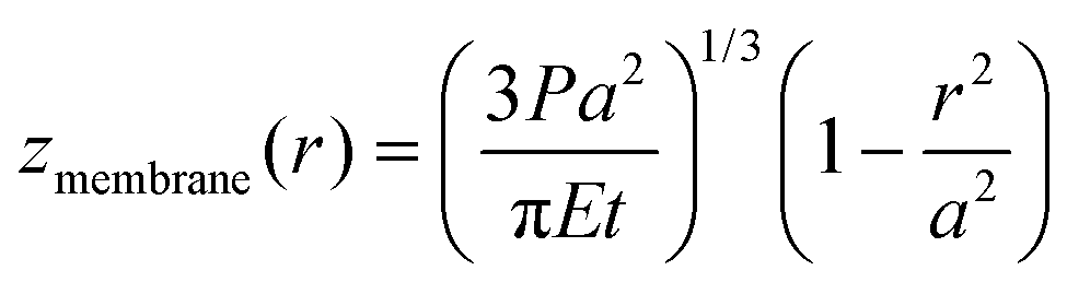
whilst the linear plate model solely considers out-of-plane bending, giving the deflection as| |  | (2) |
where P, ν and E are the applied pressure, Poisson's ratio and Young's modulus of the membrane and geometric parameters z, r, a and t are the membrane deflection, radial position, radius and thickness respectively as shown in Fig. 2. Both of these models have been proven to be accurate for freestanding polymer and graphene sheets of varying thickness.24,26–28 However, there is no analytical solution for the intermediate case where z ≤ t, which applies for many cases throughout this study. An alternative analysis of membrane deformations is to consider the deflection profile as an arc described by the equation of a circle.29 This geometric consideration allows us to express the in-plane stress σr and radial strain εr using the expressions| |  | (3) |
and| |  | (4) |
where z0 is the maximum deflection point of the micro-blister. Finite element simulations have shown that this method gives the elastic properties of deflected films within 10% accuracy.20 From these values the 2d in-plane modulus of the membrane is given by E2d = (1 − νeff)σr/εr where νeff is the effective Poisson's ratio of the heterostructure membrane (a detailed discussion regarding the effective elastic constants of this heterostructure system is given in Discussion S1†). Assuming good stress transfer between graphene and the polymer layer, the Voigt upper bound mixing rule is used to deduce the elastic modulus of the heterostructure for different polymer thicknesses.30 We validated this assumption by comparing the deflection profile of a 20 nm thick graphene–polymer heterostructure to the strain deduced from Raman spectroscopy measurements, as demonstrated in ESI Fig. S2b.† For a graphene–polymer heterostructure membrane this mixing rule reduces to Ebulk = Egϕg − Epϕp where the subscripts relate to the bulk modulus, E, and volume fraction, ϕ, of graphene (g) and polymer (p) components respectively. Here the bulk modulus is related to the 2d in-plane modulus by E2d = Ebulkt. We recognise that this two-layer model is very simplistic and may not capture all of the material properties in the membranes, such as viscoelastic effects, for example. However, the mixing rule appears to be a reasonable first approximation that accounts for the polymer thickness dependent in-plane modulus variation. Using the maximum deflection point at a given pressure from our blister inflation experiments we calculate the stress and strain using eqn (3) and (4) respectively. Fig. 3a shows the stress–strain behaviour of bare graphene and graphene–polymer heterostructures of thicknesses 20 nm, 102 nm and 207 nm, representative of the typical behaviour of the samples measured. We observed a linear stress–strain relationship across all devices for pressures above 80 kPa. At low pressures, bare graphene and 20 ± 3 nm membranes show non-linear stress–strain behaviour. Recent reports have shown that in bare graphene this membrane softening primarily originates from static wrinkling due to membrane transfer strains.20 We expect the same effect to occur for 23 ± 5 nm membranes as significant rippling is observed. Moreover, the linear stress–strain behaviour of thicker membranes is also consistent with the membrane morphologies shown in Fig. 1c. Fig. 3b shows the 2d in-plane modulus, and the E2d extracted from all measured devices. First, we note that values extracted for bare graphene are consistent with the membrane model given in eqn (1); for bare graphene samples, we measured E2d = 173 ± 55 in the pressure range 80–320 kPa. This is in agreement with a value of E2d = 215 ± 20 N m−1, calculated from the membrane model including corrections for sidewall adhesion. Similarly, the value for 210 ± 35 nm thick membranes, E2d = 1048 ± 66 N m−1 agrees with calculations based on the plate model, E2d = 1127 ± 43 N m−1. For these calculations we used values for the thickness of graphene tg = 0.335 nm and the Poisson ratio of graphene and Parylene-C as νg = 0.16 and νg = 0.4 respectively.31–33Fig. 3c shows the experimental and modelled deflection profiles of bare graphene and a 211 nm thick graphene–polymer heterostructure pressurised to give approximately the same maximum deflection point. The modelled plate and membrane deflection profiles are calculated using eqn (1) and (2) respectively. As well as validating the fit to the modified membrane and plate models, this demonstrates the ability to tune the shape of the deflected membranes by changing only the thickness and pressure load. Furthermore, the validation of the stress–strain analysis for the upper and lower limits of membrane thicknesses implies that the same method is accurate for membranes of intermediate thickness from 18 to 109 nm, for which both models become invalid. We note that the membrane model begins to diverge from the data points at the edges of the membrane. This is attributed to intrinsic crumpling of the membranes at low pressures.20 The stress–strain curves in Fig. 3a not only give the biaxial modulus, but also the pre-stress σr (at equilibrium) as the intercept. However, due to the formation of ripples near equilibrium pressures, we were unable to extract reliable pre-stress values. Fig. 3d shows the elastic modulus of all membranes measured against their corresponding volume fraction of graphene. The data points in Fig. 3d were extracted from the linear fit to data points in Fig. 3a and the respective thickness of each of the measured membrane. In total we probed 50 individual membranes of which the deflections at 10 different pressures were probed. The bulk modulus of each membrane is given by E2d = Ebulkt, where E2d is given by the gradient of the linear regression to each membrane stress–strain plot by the respective membrane thickness. We obtain the graphene volume fraction,  from the graphene and polymer layer thickness, tg and tp of each measured membrane respectively. By fitting the Voigt upper bound mixing rule to the measured data we extract the bulk elastic modulus of bare graphene and Parylene-C as Eg = 751 ± 95 GPa and Ep = 4.6 ± 0.5 GPa respectively from the y-axis intercepts. Whilst the accepted value for the intrinsic in-plane modulus of graphene is 1 TPa,33 reports have shown that this value can vary from as low as 59 GPa up to 1150 GPa, depending on the method and the pressure range in which the in-plane modulus is probed.20,34,35 The small values of in-plane modulus have been attributed to flattening out of intrinsic crumples at low pressure ranges.20 Our measurements are taken in a relatively high pressure range in which we expect minimal contributions due to intrinsic crumpling. Additional membrane softening contributions due to defects are considered negligible as Raman spectroscopy measurements indicate low defect concentrations for bare graphene as well as graphene–polymer heterostructure samples (ESI Fig. S2a†). With this taken into consideration, the extracted value of Eg = 751 ± 95 GPa is in good agreement with previous reports. For Parylene-C, the value of Ep = 4.6 ± 0.5 GPa is higher than the published value of 2.8 GPa.36 This discrepancy is attributed to stiffening of the polymer top surface layer during the fabrication process; we expect plasma–polymer interactions during oxygen plasma etching of the graphene–copper substrate to induce vacuum ultra-violet surface modifications, resulting in cross-linking in the top surface of the polymer. This stiffening effect has been measured in polystyrene (PS) and PMMA and is expected to also occur in Parylene-C.37 An additional contribution to the surface stiffening is expected from mechanical instabilities as the polymer thickness tends to zero. Molecular dynamics simulations have shown that polymer films below thicknesses of approximately 40 nm show a rapid drop in their bulk elastic modulus as the structural integrity of the polymer network begins to break down.38 However, the large variation in the elastic modulus of bare graphene masks this contribution and is therefore insignificant to our model. Previous reports on probing the elastic properties of graphene–polymer composites observed slippage at the graphene–polymer interface at a critical strain εc; McKenna et al. measured a poly(methyl methacrylate) (PEMA)–CVD graphene–PEMA sandwich structure with εc = 0.18% using a blister inflation experiment,17 whilst Kinloch et al. measured the strain of an exfoliated graphene flake sandwiched between layers of SU-8 photoresist and PMMA using Raman spectroscopy to deduce εc = 0.4%.15 In our micro-blister inflation experiments we did not observe any reproducible slippage artefacts within our range of loadings. It is likely that
the polymer in the thinnest heterostructure membrane does not have sufficient mechanical stability to induce slipping at the graphene–polymer interface. As for thicker heterostructure membranes, the applied strain at the maximum pressure (400 kPa) is below 0.4%. In this relatively low range of strains we are likely to be operating below the critical strain value of the graphene–Parylene-C interface. The stress–strain responses of two membranes under higher loadings, demonstrating slippage artefacts, are shown in ESI Fig. S4.†
from the graphene and polymer layer thickness, tg and tp of each measured membrane respectively. By fitting the Voigt upper bound mixing rule to the measured data we extract the bulk elastic modulus of bare graphene and Parylene-C as Eg = 751 ± 95 GPa and Ep = 4.6 ± 0.5 GPa respectively from the y-axis intercepts. Whilst the accepted value for the intrinsic in-plane modulus of graphene is 1 TPa,33 reports have shown that this value can vary from as low as 59 GPa up to 1150 GPa, depending on the method and the pressure range in which the in-plane modulus is probed.20,34,35 The small values of in-plane modulus have been attributed to flattening out of intrinsic crumples at low pressure ranges.20 Our measurements are taken in a relatively high pressure range in which we expect minimal contributions due to intrinsic crumpling. Additional membrane softening contributions due to defects are considered negligible as Raman spectroscopy measurements indicate low defect concentrations for bare graphene as well as graphene–polymer heterostructure samples (ESI Fig. S2a†). With this taken into consideration, the extracted value of Eg = 751 ± 95 GPa is in good agreement with previous reports. For Parylene-C, the value of Ep = 4.6 ± 0.5 GPa is higher than the published value of 2.8 GPa.36 This discrepancy is attributed to stiffening of the polymer top surface layer during the fabrication process; we expect plasma–polymer interactions during oxygen plasma etching of the graphene–copper substrate to induce vacuum ultra-violet surface modifications, resulting in cross-linking in the top surface of the polymer. This stiffening effect has been measured in polystyrene (PS) and PMMA and is expected to also occur in Parylene-C.37 An additional contribution to the surface stiffening is expected from mechanical instabilities as the polymer thickness tends to zero. Molecular dynamics simulations have shown that polymer films below thicknesses of approximately 40 nm show a rapid drop in their bulk elastic modulus as the structural integrity of the polymer network begins to break down.38 However, the large variation in the elastic modulus of bare graphene masks this contribution and is therefore insignificant to our model. Previous reports on probing the elastic properties of graphene–polymer composites observed slippage at the graphene–polymer interface at a critical strain εc; McKenna et al. measured a poly(methyl methacrylate) (PEMA)–CVD graphene–PEMA sandwich structure with εc = 0.18% using a blister inflation experiment,17 whilst Kinloch et al. measured the strain of an exfoliated graphene flake sandwiched between layers of SU-8 photoresist and PMMA using Raman spectroscopy to deduce εc = 0.4%.15 In our micro-blister inflation experiments we did not observe any reproducible slippage artefacts within our range of loadings. It is likely that
the polymer in the thinnest heterostructure membrane does not have sufficient mechanical stability to induce slipping at the graphene–polymer interface. As for thicker heterostructure membranes, the applied strain at the maximum pressure (400 kPa) is below 0.4%. In this relatively low range of strains we are likely to be operating below the critical strain value of the graphene–Parylene-C interface. The stress–strain responses of two membranes under higher loadings, demonstrating slippage artefacts, are shown in ESI Fig. S4.†
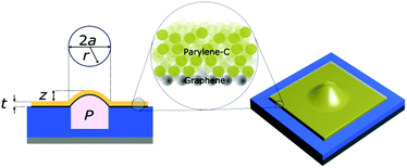 |
| | Fig. 2 A cross-section and 3-dimensional schematic of a graphene–Parylene-C heterostructure blister of thickness t, maximum deflection z, cavity radius a, under uniform static pressure P. | |
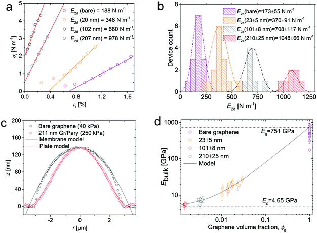 |
| | Fig. 3 (a) Stress–strain plots representing the typical behaviour of bare graphene and graphene–polymer heterostructures. (b) Statistical distribution of E2d of all samples measured. (c) The experimental and modelled deflection profiles of a bare graphene and a 211 nm thick membrane. (d) The bulk biaxial modulus for different volume fractions of graphene is fitted to the Voigt upper bound mixing rule. The two horizontal dashed lines indicate the extracted Ebulk values for bare CVD graphene and bulk Parylene-C obtained from the y-axis intercepts. The error bars are obtained from the standard error of the linear regression in (a). Several error bars have been removed to improve the clarity of the figure. | |
Several consistency checks were carried out in order to rule out any measurement artefacts. First, we repeatedly inflated and deflated membranes until negligible deflection hysteresis was measured. We found that after cycling membranes between 0 and 400 kPa more than five times, the maximum deflection point was reproducible to 0.05% of the total value. Second, we fabricated bare graphene and 20 nm membranes of diameter 2, 4, 6, 9 and 12 μm respectively, to check for consistency in the in-plane modulus. We found that membranes larger than 6 μm gave consistent values that were within the experimental error. Third, we compared blister inflation measurements with nanoindentation measurements on the same membranes. Consistency was found in the E2d for low loading forces <1 μN for bare graphene devices, demonstrating negligible influence of the direction of the membrane deflection. For larger loading forces a significantly stiffer E2d was measured. This stiffening is attributed to crumpling of the membrane as discussed earlier; in-plane stretching of the membrane becomes dominant over relaxation of static wrinkles at high loadings.20 Similar findings were observed for 20 nm thick membranes; however, complex tip–surface interactions with the polymer surface limited the accuracy of the force-curve fitting. These interactions were pronounced for thicker polymers and higher loads. Therefore, the comparative study was restricted to bare graphene membranes only (an outline of AFM nanoindentation studies is given in ESI Fig. S3 and Discussion S5†).
2.3 Electrical conductivity
The sheet resistance of bare graphene and graphene–polymer heterostructures was probed by transmission line measurements (TLM) as shown in Fig. 4a and b. Gold electrode TLM structures of 50 nm thickness, with contact spacing between 5 μm and 80 μm were patterned onto a Si/SiO2 wafer. A series of patterned strips consisting of bare graphene, 20 nm and 210 nm thick graphene–polymer heterostructures with a width of 50 μm were then transferred onto the TLM structure. Each sample was baked in air for 30 minutes at 110 °C to allow the polymer to conform to the substrate, whilst preventing thermal cross-linking of the Parylene-C.36 The total resistance as a function of contact separation was measured to a gate bias of 10 mV and 20 nA source–drain current and is shown in Fig. 4b. The extracted sheet resistance Rsh of bare graphene, 20 nm and 210 nm graphene–polymer heterostructures is 2.78 kΩ □−1, 5.34 kΩ □−1 and 6.38 kΩ □−1 respectively and show good agreement with recent reports.39 It is inappropriate to compare these resistance values with the current state of the art silicon-based MEMS components due to the orders of magnitude difference in thickness. For example, a typical doped silicon pressure sensor with a total membrane thickness of 60 μm spanning a 1.4 mm × 1.4 mm cavity has Rsh = 140 Ω □−1.40 Instead we compare our results to other ultra-thin membrane composites to reveal a significant improvement; gold nanoparticle membranes of thickness 55 nm and carbon nano-membranes of thickness 1 nm have Rsh = 1.8 MΩ □−1 and 20 kΩ □−1 respectively.41 In conclusion, we look towards applying these structures either in low frequency applications where low resistance is not critical, or alternatively, multiple graphene layers may be integrated into the heterostructure to improve the sheet resistance.42
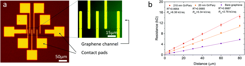 |
| | Fig. 4 (a) Optical micrograph with enlargement of a TLM structure with a 20 nm thick graphene–polymer membrane transferred on top. (b) Transmission line data of bare graphene and graphene–polymer heterostructures of thickness 20 nm and 210 nm. The sheet resistance Rsh is deduced from the gradient of the linear regression. The error bars are obtained from the standard error from the linear regression for bare CVD graphene and bulk Parylene-C obtained from the y-axis intercepts. The error bars are obtained from the standard error of the linear regression. | |
2.4 Membrane fabrication yield
Commercial devices often consist of an array of such micron-scale structures in order to improve sensitivity or provide additional aerial functionalities, such as directional sensing.43 In the following section we characterise the electrical sheet resistance as well as the fabrication yield of graphene–polymer heterostructures in view of MEMS applications. In order to validate the fabrication yield we fabricated membranes with diameters ranging from 2 μm to 30 μm using bare graphene, 20 nm, 101 nm and 210 nm thick graphene–polymer heterostructures as shown in Fig. 5a. Circular micro-cavities were etched to depths of 950 nm to eliminate membrane collapse due to stiction to the cavity bed. The yield of membranes was characterised by counting the quantity of membranes that are inflated after pressurising to 400 kPa, using the micro-blister inflation method as described above. Whilst optical inspection allows us to discriminate between fully collapsed membranes and inflated micro-blisters, it is difficult to distinguish suspended membranes that do not inflate due to nano-scale cracks. Fig. 5b shows an AFM height map of an array of 20 nm thick graphene–polymer membranes suspended across 15 μm diameter micro-cavities. This height map indicates that out of the 9 membranes probed, 3 are defect free and form micro-blisters (indicated by the white arrow (i) in Fig. 5b; the remaining 6 have collapsed (ii) or exhibit nanoscale cracks (iii) allowing gas to permeate across the membrane). Fig. 5c and d show a close packed array of 15 μm diameter membranes with a thickness of 102 ± 5 nm. The AFM height map of these membranes demonstrates that all membranes are suspended and can hold high pressures. Fig. 5e shows the yield of membranes of different thicknesses suspended over varying cavity sizes. We see a steep drop in yield beyond 5 μm diameter for bare graphene membranes, whilst for 20 nm thick membranes a yield above 80% is maintained up to 10 μm diameter. This indicates that the Parylene-C layer acts as a structural support for the graphene base layer. This trend is further pronounced for 101 nm and 210 nm thick membranes. It is important to note that the yield is highly dependent on the fabrication process and the CVD graphene quality. Thus it is inadequate to directly compare these values to previous reports.
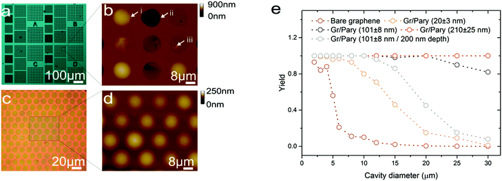 |
| | Fig. 5 (a) An optical micrograph of a 20 nm graphene–polymer heterostructure transferred onto an array of micro-cavities. Scale bar: 100 μm. (b) An AFM height map of 15 μm diameter membranes pressurised to 400 kPa. The white arrows respectively indicate the morphology of a defect free micro-blister (i), a collapsed membrane (ii) and a suspended membrane with defects (iii). The location of the scan area is indicated by the box in (a). Scale bars: 8 μm, 0 nm to 900 nm. (c) An optical micrograph of a close packed array of 15 μm diameter membranes with a thickness of 102 ± 5 nm at equilibrium pressure. Scale bar: 20 μm. (d) The magnified area in (c) shows an AFM height map of the membranes pressurised to 400 kPa. Scale bars: 8 μm, 0 nm to 250 nm. (e) The suspended membrane yield for different cavity diameters of all four membrane thicknesses. An additional plot of a 101 ± 8 nm membrane suspended over a 200 nm deep micro-cavity shows the drop in yield due to stiction effects. | |
2.5 Application of a graphene–polymer heterostructure membrane
The mechanical properties of graphene–polymer heterostructures are suitable for many active components in MEMS technologies. Existing and emerging MEMS devices employ either a silicon-based or a polymer-based actuating membrane. Below we explore the application space for the graphene–polymer membrane, outlining the current challenges faced by the existing state of the art systems and how effective the implementation of the graphene–polymer system can lead to novel devices and significant technological improvements. We have summarised the electro-mechanical properties of typical membranes in Table 1. Polymer-based membranes are generally on the order of microns in thickness and undergo large deflections at small forces, whilst silicon-based components are used in sensitive and high frequency applications. The thickness and modulus of our proposed structures places the graphene–Parylene-C heterostructure membranes and generally graphene–polymer membranes in the application space which currently includes polymer membranes, and also extends into the properties and performance gaps between polymer and silicon MEMS. Indeed, we show that graphene–polymer membranes could even compete with silicon-based MEMS for certain low-frequency applications.
Table 1 The electromechanical properties of state of the art membrane structures
| Membrane materials |
Thickness (nm) |
Diameter (μm) |
Elastic modulus (GPa) |
Sheet resistance (kΩ □−1) |
Critical strain |
|
Yield strength of Parylene-C.
Upper bound of our measurements.
|
| Parylene/gold/parylene45 |
1300/200/1300 |
300 |
4 |
<0.1 |
1.2%32![[thin space (1/6-em)]](https://www.rsc.org/images/entities/char_2009.gif) a a |
| Silicon oxide/aluminium46 |
4000/200 |
2000 |
150 |
<0.1 |
— |
| Gold nanoparticles47 |
56 |
100 |
8.9 |
0.9542 |
— |
| Carbon nano-membranes48 |
2 |
30 |
0.56 |
100 |
0.8% |
| Graphene–Parylene-C |
0.35/20 |
30 |
10.6 |
5.3 |
1.4%b |
2.5.1 Polymer-based MEMS.
Polymer-based membranes are most commonly used in the fields of microfluidics and biomedicine.44,45 The active components in these structures are commonly made of thin polymeric membranes in the range of 1 to 60 μm that have a thin metal layer (50–500 nm) embedded in their core and undergo large deformations.49 For example, a large stroke polydimethylsiloxane (PDMS) based micro-pump with an embedded 200 nm Cr/Al/Cr stack of 2 mm diameter and 56 μm thickness is strained approximately 0.7% at full stroke.50 The challenges faced by such membranes include non-reversible changes in resistance in the presence of varying strain, temperature, humidity and chemical environment.51 Additional challenges arise from stiffening of the membrane and out-of-plane stress and hysteresis due to metal film deposition onto the polymer.52 Our mechanical measurements show that graphene–polymer membranes can be strained reproducibly beyond 1% with consistent Raman spectra before and after straining. Thus we infer that no significant damage is inflicted to the graphene layer and deflections have minimal hysteresis. In addition, bare CVD graphene exhibits a relatively low gauge factor between 2–6,53 minimal intrinsic temperature-resistance dependence and is highly inert to harsh environments,54,55 hence making the structure highly suitable for the afore mentioned applications. We envisage different membrane thicknesses for different polymer-MEMS applications. For example, actuating devices such as pumps and valves are more suited to thin membranes comprising a low modulus polymer or elastomer such as PDMS. The low mass and in-plane modulus of such membranes are expected to give large deflections and excellent response times for low actuation voltages. On the other hand, for high-sensitivity devices operating in small pressure ranges, we utilise relatively high modulus polymers under pre-strain. This allows precise positioning of the membrane in close proximity to a complementary sensing electrode, whilst realising large area and high yield suspended structures. We note here that this configuration is not limited to polymer based applications and is equally valid for silicon devices.
2.5.2 Silicon-based MEMS.
Complementary metal oxide semiconductor (CMOS) processing has enabled highly reliable silicon-based MEMS that are readily integrated into digital systems.56 The active free-standing structures in these devices range in thickness from tens of nanometres (silicon nitride resonators)57 to several microns (aluminium embedded in silicon oxide)43 and have an elastic modulus and breaking strength in the range of hundreds of GPa and 1–4 GPa respectively.58 For example, a 100 nm thick polysilicon thin film has an elastic modulus of 151 ± 23 GPa. The nanometer-range thickness combined with a relatively low breaking strength, makes silicon-based suspended structures highly prone to fracture in high acceleration shock environments, calling for many shock reduction strategies in MEMS-design.59 In comparison, the elastic modulus of graphene–polymer heterostructures of similar thickness (101 nm) is significantly lower (7.2 ± 0.9 GPa), however the high breaking strength of graphene (103 GPa)33 and the 100% yield processability makes these structures excellent candidates for MEMS applications. We recognise that the strength is best represented by a distribution of values (for example using the Weibull modulus), rather than a single breaking strength value. Whilst limitations in obtaining reliable nanoindentation data (ESI Discussion S5†) prevented us from measuring the breaking strength of graphene–polymer heterostructures, the two order magnitude difference in the breaking strength of graphene over silicon suggests a significant improvement in the membrane mechanical reliability. Another challenge faced by silicon based technologies is the limited device performance for harsh environments. High operating temperatures, reactive species and radiation limit the use of silicon due to its ease of oxidation, its narrow bandgap and its susceptibility to corrosion and erosion.60 Robust and inert high temperature pressure sensors have been demonstrated up to operating temperatures of 600 °C using alternative materials such as co-fired ceramics and silicon carbide. However, the devices either have poor sensitivity or their geometry is on the order of several millimetres.60,61 In contrast, Raman spectroscopy studies confirm that single-layer graphene is defect free in air up to temperatures of 500 °C and above 600 °C for multiple layers.62 Thus, we expect the graphene–polymer heterostructure to be limited by the thermal stability of the polymer layer. Furthermore, it has been shown that graphene can even improve the thermal stability of polyimide-based nanocomposites.63 Using the model presented in this work, we show that the elastic modulus and sheet resistance of graphene-polymer heterostructures can be further tuned by using multiple layers of CVD graphene as shown in Fig. 6. This not only demonstrates the ability to further tune the electromechanical properties towards specific applications, but may also improve the elastic limit of membranes for large deflections as demonstrated in previous reports.64 The stacking of conductive CVD graphene layers also significantly improves the sheet resistance of the heterostructures. In addition further improvement can be achieved by modifying the fabrication process or doping CVD graphene.65 As an example, it has been shown that optimisation of the CVD graphene transfer onto polymer substrates by a roll-to-roll method can give a sheet resistance as low as 275 Ω □−1.66
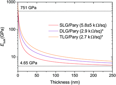 |
| | Fig. 6 The bulk biaxial modulus of different membrane thicknesses is modelled for single (SLG), double (DLG) and triple (TLG) layer graphene–Parylene-C heterostructures according to the Voigt upper bound mixing rule. The horizontal dashed lines indicate the extracted Ebulk values for bare CVD-graphene and Parylene-C from our experiments. The sheet resistance values of each of the films is given in the figure legend. *Values are estimates based on previous reports.66 | |
3. Methods
3.1 Parylene-C coating
CVD graphene grown on a 25 μm thick copper foil, purchased from BGT Materials (Gratom-M-Cu) was used for all experiments. The foil was coated in the desired thickness of Parylene-C (di(2-chloro-p-xylylen)) by chemical vapor deposition using a SCS Labcoater 2010 system with an Inficon XTC2 deposition controller. For the entire deposition the pyrolysis furnace is set to 690 °C. The deposition chamber is pumped to 15 mTorr before the vaporiser is switched on and heated up to 175 °C. The deposition is finished when the temperature (175 °C) is reached and the deposition rate is stable. The samples are kept in the chamber during the chamber cooling step. The thickness of the Praylene-C is obtained by the initial dimer weight portion. This produced conformal coatings of 23 ± 5 nm, 101 ± 8 nm, 218 ± 17 nm and 510 ± 35 nm of Parylene-C on the CVD graphene surface.
3.2 Fabrication of micro-blister devices
The uncoated side of the Parylene-C coated copper foil is first exposed to a 1 minute low power O2-Ar plasma etch to remove CVD graphene from the underside of the Cu foil. The foil was then spin-coated with a thin PMMA coating (≈200 nm) for additional support and a Kapton® tape window was pressed on top for handling. This whole structure was then placed in a 0.1 M ammonium persulfate etch bath to remove the copper from the underside of the foil. Once the copper is etched, the resulting graphene–Parylene-C–PMMA membrane is rinsed in deionized (DI) water by repeatedly transferring the membrane between individual DI water baths. On a separate substrate, circular cavities of diameter 2 to 30 μm were etched 950 nm deep into a Si/SiO2 substrate with a 1.5 μm oxide layer using a bilayer photoresist/aluminium mask for deep reactive ion etching using CHF3 and Ar gas. The cleaned membrane is then lifted out of the final DI water bath and dried in air for 30 minutes before transferring onto the patterned substrate using a custom built setup. The tape window is carefully removed by tearing the graphene–polymer stack around the area containing the cavities. The substrate is then baked at 130 °C for 10 minutes allowing the polymer membrane to soften and conform to the substrate. Finally, the PMMA layer is dissolved in acetone for 2 hours, followed by a rinse in hexane before the substrate is dried in air. On probing Parylene-C coated CVD graphene samples by AFM before PMMA coating and after PMMA removal, we found an imperceptible change in the Parylene-C surface morphology. In addition, the PMMA residues on SiO2 substrates (which have a similar adhesion to PMMA as Parylene-C)67,68 show negligible traces of PMMA after the same removal procedure as above.
3.3 Micro-blister inflation
The inflation of micro-blisters was conducted by inserting samples into a pressure chamber equipped with a commercial reference pressure sensor (MKS Baratron 722B) and a gate valve (MKS instruments T3Bi) that allows precise control over the chamber pressure. To ensure that multiple deflections of the same membrane are reproducible, samples were cycled between 0 kPa and 100 kPa multiple times to partially release pre-tension from the fabrication process. The blister inflation process is shown in Fig. 1b. The chamber was pumped with N2 gas to the desired pressure and then left for 24 hours in order for the N2 gas to diffuse into the micro-cavities, equilibrating the pressure across the membrane. The samples were removed from the pressure chamber, causing the membrane to form a blister above the micro-cavity. Within 5 minutes of removing the samples from the pressure chamber they were mounted onto an AFM and the cross-sections of the micro-blisters were probed. We continued to monitor the cross-section of the micro-blisters in 17 minute intervals over 3 hours after pressurisation, as the N2 gas slowly leaks out of the micro-cavity. This allowed us to correct for the decrease in blister deflection between the time of removing the sample from the pressure chamber to scanning the blister cross-section on the AFM (ESI Fig. S1†). Depending on the thickness of the heterostructure membranes, blisters took between 2 and 18 hours to deflate to within 10% of their zero deflection point.
3.4 Fabrication of transmission line devices
For electrical measurements we begin by transferring bare CVD graphene onto a blank Si/SiO2 substrate using the same transfer process as above. The graphene is then patterned into a 50 μm wide strip using a photoresist mask and O2 plasma etching. The photoresist is then cleaned off and a layer of Parylene-C is deposited. The graphene–polymer stack is then released from the substrate by submerging the substrate in a 20% potassium hydroxide solution, causing the silicon oxide layer to be etched away. The membrane is then transferred in consecutive DI water baths to remove any remaining etchant. On a separate substrate, the transmission line electrode structure is defined using a photomask followed by thermal evaporation of a 2 nm/50 nm chromium/gold stack. The photomask is then cleaned off with acetone and the substrate is plasma cleaned. We accurately align the patterned graphene–polymer heterostructure membrane with the TLM electrodes and proceed with the same transfer steps as for the micro-blister structure described above.
3.5 Yield characterisation
We analysed over 400 membranes across 4 separate samples for each membrane diameter up to 10 μm for each membrane thickness. Beyond 10 μm we analysed 40 membranes over 4 individual samples for each membrane geometry.
3.6 Thickness determination of graphene–polymer heterostructure
A strip of Kapton® tape was stuck down and removed within 20 μm of the membranes. On removal of the tape the bare substrate is exposed, giving an accurate zero height reference for determining the membrane thickness. The thickness of each measured membrane was then determined by scanning a 50 μm × 50 μm area at the edge of the tear in proximity to the membranes. An example of this measurement is given in ESI Fig. S5.†
3.7 PeakForce™ atomic force microscopy
A Bruker Dimension ICON AFM equipped with a SCANASYST-FLUID+ probe was used to perform AFM height measurements in ScanAsyst™ imaging mode. For imaging suspended bare graphene the applied tip force during imaging was kept below 10 nN to avoid damage to the membranes. For graphene–polymer heterostructures the tip force was kept below 50 nN.
4. Conclusions
We have demonstrated the fabrication and mechanical and electrical characterisation of ultra-thin graphene-polymer heterostructure membranes. The fabrication method enables the construction of suspended structures that can be multiplexed over a wafer scale with 100% yield. We have measured the in-plane elastic modulus of the membranes with thicknesses from 18 nm to 235 nm. The deflections of these membranes reveal a change in the membrane morphology as a function of pressure and thickness. The variation of the in-plane modulus as a function of thickness is in good agreement with the Voigt upper bound mixing rule, ranging from the 2d modulus of bare graphene of 173 ± 55 N m−1, consistent with the literature values, to the bulk elastic modulus of Parylene-C of 4.6 ± 0.5 GPa, which is significantly higher than reported in the literature. We attribute this discrepancy to fabrication induced stiffening of the polymer top–surface.
Looking forward, we aim to develop a more sophisticated analytical model to describe the elastic properties of ultra-thin graphene–polymer heterostructure membranes. By considering the polymer layer alone as a bilayer system we aim to correct the mixing rule applied above to account for surface stiffening. Moreover, an improved description of the mechanical properties of these structures allows us to model the performance of next generation graphene–polymer MEMS. We envisage the use of graphene–polymer heterostructures primarily in polymer MEMS devices ranging from micron-scale pumps and valves in micro-fluidics and Lab-on-Chip devices to pressure and strain sensors in biomedical applications.
Graphene–Parylene-C heterostructure membranes pave the way for more advanced graphene–polymer layered composites. The large variety of polymers available as ultra-thin coatings to date allow us to fabricate a range of ultra-thin conductive membranes with properties tuned to specific applications, where the polymer layer not only acts as a mechanical reinforcement but also gives additional functionality to the membrane.69,70 Equally, other emerging 2d materials or modified graphene can be implemented in place of CVD graphene in order to realise applications beyond MEMS. For example, novel polymers and 2d material heterostructures could be used to enhance fuel cell membranes or nano-filtration technologies in which 2d materials have already shown much promise.71
Acknowledgements
AV and CB acknowledge funding from EPSRC Industrial Cooperative Awards in Science & Technology (CASE). Authors acknowledge support from Ashley Nathan Smith and Danial Collyer of Merck Chemicals Ltd and Simone Dehm and Ralph Krupke of the Micro-structure Technology Institute at Karlsruhe Institute of Technology (KIT) for Parylene-C coatings.
Notes and references
- A. D. Smith, F. Niklaus, A. Paussa, S. Vaziri, A. C. Fischer, M. Sterner, F. Forsberg, A. Delin, D. Esseni, P. Palestri, M. Östling and M. C. Lemme, Nano Lett., 2013, 13, 3237–3242 CrossRef CAS PubMed.
- A. M. van der Zande, R. A. Barton, J. S. Alden, C. S. Ruiz-Vargas, W. S. Whitney, P. H. Q. Pham, J. Park, J. M. Parpia, H. G. Craighead and P. L. McEuen, Nano Lett., 2010, 10, 4869–4873 CrossRef CAS PubMed.
- C. Lee, X. Wei, J. W. Kysar and J. Hone, Science, 2008, 321, 3885–3888 Search PubMed.
- X. Li, W. Cai, J. An, S. Kim, J. Nah, D. Yang, R. Piner, A. Velamakanni, I. Jung, E. Tutuc, S. K. Banerjee, L. Colombo and R. S. Ruoff, Science, 2009, 324, 1312–1324 CrossRef CAS PubMed.
- J. W. Suk, A. Kitt, C. W. Magnuson, Y. Hao, S. Ahmed, J. An, A. K. Swan, B. B. Goldberg and R. S. Ruoff, ACS Nano, 2011, 5, 6916–6924 CrossRef CAS PubMed.
- J. S. Bunch, S. S. Verbridge, J. S. Alden, A. M. van der Zande, J. M. Parpia, H. G. Craighead and P. L. McEuen, Nano Lett., 2008, 8, 2458–2462 CrossRef CAS PubMed.
- O. I. Aydin, T. Hallam, J. L. Thomassin, M. Mouis and G. Duesberg, IEEE Ultim. Integr. Silicon, 2014, 33–36 Search PubMed.
- T. Hallam, C. F. Moldovan, K. Gajewski, A. M. Ionescu and G. S. Duesberg, Phys. Status Solidi, 2015, 252, 2429–2432 CrossRef CAS.
- T. Hallam, N. C. Berner, C. Yim and G. S. Duesberg, Adv. Mater. Interfaces, 2014, 1, 1400115 CrossRef.
- L. D. Qiugu Wang and W. Hong, Nanoscale, 2016, 8, 7663–7671 RSC.
- A. M. Hurst, S. Lee, N. Petrone, J. Vandeweert, A. M. Van Der Zande and J. Hone, IEEE Transducers, 2013, 586–589 CAS.
- K. Celebi, J. Buchheim, R. M. Wyss, A. Droudian, P. Gasser, I. Shorubalko, J.-I. Kye, C. Lee and H. G. Park, Science, 2014, 344, 289–292 CrossRef CAS PubMed.
- T. M. G. Mohiuddin, A. Lombardo, R. R. Nair, A. Bonetti, G. Savini, R. Jalil, N. Bonini, D. M. Basko, C. Galiotis, N. Marzari, K. S. Novoselov, A. K. Geim and A. C. Ferrari, Phys. Rev. B: Condens. Matter, 2009, 79, 205433 CrossRef.
- A. P. A. Raju, A. Lewis, B. Derby, R. J. Young, I. A. Kinloch, R. Zan and K. S. Novoselov, Adv. Funct. Mater., 2014, 24, 2865–2874 CrossRef CAS.
- L. Gong, I. A. Kinloch, R. J. Young, I. Riaz, R. Jalil and K. S. Novoselov, Adv. Mater., 2010, 22, 2694–2697 CrossRef CAS PubMed.
- D. Metten, F. Federspiel, M. Romeo and S. Berciaud, Phys. Rev. Appl., 2014, 2, 054008 CrossRef.
- Z. Cao, P. Wang, W. Gao, L. Tao, J. W. Suk, R. S. Ruoff, D. Akinwande, R. Huang and K. M. Liechti, Carbon, 2014, 69, 390–400 CrossRef CAS.
- X. Li, J. Warzywoda and G. B. McKenna, Polymer, 2014, 55, 4976–4982 CrossRef CAS.
- Z. Cao, L. Tao, D. Akinwande, R. Huang and K. M. Liechti, J. Appl. Mech., 2015, 82, 081008 CrossRef.
- R. J. T. Nicholl, H. J. Conley, N. V. Lavrik, I. Vlassiouk, Y. S. Puzyrev, V. P. Sreenivas, S. T. Pantelides and K. I. Bolotin, Nat. Commun., 2015, 6, 8789 CrossRef CAS PubMed.
- F. Scarpa, S. Adhikari and A. Srikantha Phani, Nanotechnology, 2009, 20, 065709 CrossRef CAS PubMed.
- N. Clark, A. Oikonomou and A. Vijayaraghavan, Phys. Status Solidi, 2013, 250, 2672–2677 CrossRef CAS.
- U. Komaragiri, M. R. Begley and J. G. Simmonds, J. Appl. Mech., 2005, 72, 203–212 CrossRef.
- S. P. Koenig, N. G. Boddeti, M. L. Dunn and J. S. Bunch, Nat. Nanotechnol., 2011, 6, 543–546 CrossRef CAS PubMed.
- C.-L. Chen, E. Lopez, Y.-J. Jung, S. Müftü, S. Selvarasah and M. R. Dokmeci, Appl. Phys. Lett., 2008, 93, 093109 CrossRef.
- Z. Cao, L. Tao, D. Akinwande, R. Huang and K. M. Liechti, Int. J. Solids Struct., 2015, 84, 147–159 CrossRef.
- K. C. Maner, M. R. Begley and W. C. Oliver, Acta Mater., 2004, 52, 5451–5460 CrossRef CAS.
- D. A. Hardwick and S. Diego, Thin Solid Films, 1987, 154, 109–124 CrossRef CAS.
- M. K. Small and W. D. Nix, J. Mater. Res., 1992, 7, 1553–1563 CrossRef CAS.
- H. Kim, A. A. Abdala and C. W. Macosko, Macromolecules, 2010, 43, 6515–6530 CrossRef CAS.
- Y. Huang, J. Wu and K. C. Hwang, Phys. Rev. B: Condens. Matter, 2006, 74, 245413 CrossRef.
- C. Y. Shih, T. A. Harder and Y. C. Tai, Microsyst. Technol., 2004, 10, 407–411 CrossRef CAS.
- C. S. Ruiz-Vargas, H. L. Zhuang, P. Y. Huang, A. M. Van Der Zande, S. Garg, P. L. Mceuen, D. A. Muller, R. G. Hennig and J. Park, Nano Lett., 2011, 11, 2259–2263 CrossRef CAS PubMed.
- G.-H. Lee, R. C. Cooper, S. J. An, S. Lee, A. van der Zande, N. Petrone, A. G. Hammerberg, C. Lee, B. Crawford, W. Oliver, J. W. Kysar and J. Hone, Science, 2013, 340, 1073–1076 CrossRef CAS PubMed.
- J. Lee, D. Yoon and H. Cheong, Nano Lett., 2012, 12, 4444–4448 CrossRef CAS PubMed.
- R. P. von Metzen and T. Stieglitz, Biomed. Microdevices, 2013, 15, 727–735 CrossRef PubMed.
- G. S. Oehrlein, R. J. Phaneuf and D. B. Graves, J. Vac. Sci. Technol., B, 2011, 29, 010801 Search PubMed.
- T. R. Böhme and J. J. de Pablo, J. Chem. Phys., 2002, 116, 9939 CrossRef.
- A. Gahoi, V. Passi, S. Kataria, S. Wagner, A. Bablich and M. C. Lemme, Solid State Device Res. Conf., 2015, 184–187 Search PubMed.
- X. Li, Q. Liu, S. Pang, K. Xu, H. Tang and C. Sun, Sens. Actuators, A, 2012, 179, 277–282 CrossRef CAS.
- H. Schlicke, M. Rebber, S. Kunze and T. Vossmeyer, Nanoscale, 2015, 8, 183–186 RSC.
- H. J. Park, J. Meyer, S. Roth and V. Skákalová, Carbon., 2010, 48, 1088–1094 CrossRef CAS.
- C.-L. Dai, P.-W. Lu, C. Chang and C.-Y. Liu, Sensors, 2009, 9, 10158–10170 CrossRef CAS PubMed.
- I. E. Araci and P. Brisk, Curr. Opin. Biotechnol., 2014, 25, 60–68 CrossRef CAS PubMed.
- D. Ha, W. N. de Vries, S. W. M. John, P. P. Irazoqui and W. J. Chappell, Biomed. Microdevices, 2012, 14, 207–215 CrossRef CAS PubMed.
- M. Goto, Y. Iguchi, K. Ono, A. Ando, F. Takeshi, S. Matsunaga, Y. Yasuno, K. Tanioka and T. Tajima, Sensors, 2007, 7, 4–10 CrossRef.
- H. Schlicke, D. Battista, S. Kunze, C. J. Schröter, M. Eich and T. Vossmeyer, ACS Appl. Mater. Interfaces, 2015, 7, 15123–15128 CAS.
- S. Markutsya, C. Jiang, Y. Pikus and V. V. Tsukruk, Adv. Funct. Mater., 2005, 15, 771–780 CrossRef CAS.
- H. Kim, A. A. Astle, K. Najafi, L. P. Bernal and P. D. Washabaugh, J. Microelectromech. Syst., 2015, 24, 192–206 CrossRef CAS.
- J. Gao, D. Guo, S. Santhanam and G. K. Fedder, J. Microelectromech. Syst., 2015, 24, 2170–2177 CrossRef.
- C. Liu, Adv. Mater., 2007, 19, 3783–3790 CrossRef CAS.
- D. Sameoto, S. Tsang and M. Parameswaran, Sens. Actuators, A, 2010, 134, 457–464 CrossRef.
- J. Zhao, G.-Y. Zhang and D.-X. Shi, Chin. Phys. B, 2013, 22, 057701 CrossRef.
- J. Chan, A. Venugopal, A. Pirkle, S. Mcdonnell, D. Hinojos, C. W. Magnuson, R. S. Ruoff, L. Colombo, R. M. Wallace, E. M. Vogel and C. E. T. Al, ACS Nano, 2012, 6, 3224–3229 CrossRef CAS PubMed.
- S. Chen, L. Brown, M. Levendorf, W. Cai, S. Ju, J. Edgeworth, R. S. Ruoff and C. E. T. Al, ACS Nano, 2011, 5, 1321–1327 CrossRef CAS PubMed.
- J. C. Greenwood, J. Phys. E: Sci. Intrum., 1988, 21, 1114–1128 CrossRef CAS.
- S. Schmid, T. Bagci, E. Zeuthen, J. M. Taylor, P. K. Herring, M. C. Cassidy, C. M. Marcus, L. Guillermo Villanueva, B. Amato, A. Boisen, Y. Cheol Shin, J. Kong, A. S. Sørensen, K. Usami and E. S. Polzik, J. Appl. Phys., 2014, 115, 054513 CrossRef.
- T. Tanemura, S. Yamashita, H. Wado and Y. Takeuchi, Jpn. J. Appl. Phys., 2012, 51, 1–7 CrossRef.
- K. Xu, N. Zhu, X. Zhang, W. Su, W. Zhang and Y. Hao, MEMS, 2016, 2016, 1125–1128 Search PubMed.
- N. Marsi, B. Y. Majlis, A. A. Hamzah and F. Mohd-Yasin, Microsyst. Technol., 2014, 21, 319–330 CrossRef.
- J. Xiong, Y. Li, Y. Hong, B. Zhang, T. Cui, Q. Tan, S. Zheng and T. Liang, Sens. Actuators, A, 2013, 197, 30–37 CrossRef CAS.
- H. Y. Nan, Z. H. Ni, J. Wang, Z. Zafar, Z. X. Shi and Y. Y. Wang, J. Raman Spectrosc., 2013, 44, 1018–1021 CrossRef CAS.
- M. Yoonessi, Y. Shi, D. A. Scheiman, M. Lebron-colon, D. M. Tigelaar, R. A. Weiss, M. A. Meador, U. States and N. Glenn, ACS Nano, 2012, 7644–7655 CrossRef CAS PubMed.
- S. Won, Y. Hwangbo, S.-K. Lee, K.-S. Kim, K.-S. Kim, S.-M. Lee, H.-J. Lee, J.-H. Ahn, J.-H. Kim and S.-B. Lee, Nanoscale, 2014, 6, 6057–6064 RSC.
- C. Wang, Y. Chen, K. Zhuo and J. Wang, Chem. Commun., 2013, 49, 3336–3338 RSC.
- S. Bae, H. Kim, Y. Lee, X. Xu, J.-S. Park, Y. Zheng, J. Balakrishnan, T. Lei, H. R. Kim, Y. Il Song, Y.-J. Kim, K. S. Kim, B. Ozyilmaz, J.-H. Ahn, B. H. Hong and S. Iijima, Nat. Nanotechnol., 2010, 5, 574–578 CrossRef CAS PubMed.
- F. T. Tsai, C. T. Chuang, T. C. Li and P. C. Yu, Appl. Mech. Mater., 2012, 217–219, 1077–1082 CrossRef CAS.
-
A. Pizzi and K. L. Mittal, Handbook of Adhesive Technology, Revised and Expanded, CRC Press, 2003 Search PubMed.
- A. Castellanos-Gomez, V. Singh, H. S. J. van der Zant and G. A. Steele, Ann. Phys., 2015, 527, 27–44 CrossRef CAS.
- C. M. Stafford, B. D. Vogt, C. Harrison, R. V. April, V. Re, M. Recei and V. June, Macromolecules, 2006, 39, 5095–5099 CrossRef CAS.
- S. P. Koenig, L. Wang, J. Pellegrino and J. S. Bunch, Nat. Nanotechnol., 2012, 7, 728–732 CrossRef CAS PubMed.
Footnote |
| † Electronic supplementary information (ESI) available. See DOI: 10.1039/c6nr06316k |
|
| This journal is © The Royal Society of Chemistry 2016 |

 Open Access Article
 This Open Access Article is licensed under a


 from the graphene and polymer layer thickness, tg and tp of each measured membrane respectively. By fitting the Voigt upper bound mixing rule to the measured data we extract the bulk elastic modulus of bare graphene and Parylene-C as Eg = 751 ± 95 GPa and Ep = 4.6 ± 0.5 GPa respectively from the y-axis intercepts. Whilst the accepted value for the intrinsic in-plane modulus of graphene is 1 TPa,33 reports have shown that this value can vary from as low as 59 GPa up to 1150 GPa, depending on the method and the pressure range in which the in-plane modulus is probed.20,34,35 The small values of in-plane modulus have been attributed to flattening out of intrinsic crumples at low pressure ranges.20 Our measurements are taken in a relatively high pressure range in which we expect minimal contributions due to intrinsic crumpling. Additional membrane softening contributions due to defects are considered negligible as Raman spectroscopy measurements indicate low defect concentrations for bare graphene as well as graphene–polymer heterostructure samples (ESI Fig. S2a†). With this taken into consideration, the extracted value of Eg = 751 ± 95 GPa is in good agreement with previous reports. For Parylene-C, the value of Ep = 4.6 ± 0.5 GPa is higher than the published value of 2.8 GPa.36 This discrepancy is attributed to stiffening of the polymer top surface layer during the fabrication process; we expect plasma–polymer interactions during oxygen plasma etching of the graphene–copper substrate to induce vacuum ultra-violet surface modifications, resulting in cross-linking in the top surface of the polymer. This stiffening effect has been measured in polystyrene (PS) and PMMA and is expected to also occur in Parylene-C.37 An additional contribution to the surface stiffening is expected from mechanical instabilities as the polymer thickness tends to zero. Molecular dynamics simulations have shown that polymer films below thicknesses of approximately 40 nm show a rapid drop in their bulk elastic modulus as the structural integrity of the polymer network begins to break down.38 However, the large variation in the elastic modulus of bare graphene masks this contribution and is therefore insignificant to our model. Previous reports on probing the elastic properties of graphene–polymer composites observed slippage at the graphene–polymer interface at a critical strain εc; McKenna et al. measured a poly(methyl methacrylate) (PEMA)–CVD graphene–PEMA sandwich structure with εc = 0.18% using a blister inflation experiment,17 whilst Kinloch et al. measured the strain of an exfoliated graphene flake sandwiched between layers of SU-8 photoresist and PMMA using Raman spectroscopy to deduce εc = 0.4%.15 In our micro-blister inflation experiments we did not observe any reproducible slippage artefacts within our range of loadings. It is likely that
the polymer in the thinnest heterostructure membrane does not have sufficient mechanical stability to induce slipping at the graphene–polymer interface. As for thicker heterostructure membranes, the applied strain at the maximum pressure (400 kPa) is below 0.4%. In this relatively low range of strains we are likely to be operating below the critical strain value of the graphene–Parylene-C interface. The stress–strain responses of two membranes under higher loadings, demonstrating slippage artefacts, are shown in ESI Fig. S4.†
from the graphene and polymer layer thickness, tg and tp of each measured membrane respectively. By fitting the Voigt upper bound mixing rule to the measured data we extract the bulk elastic modulus of bare graphene and Parylene-C as Eg = 751 ± 95 GPa and Ep = 4.6 ± 0.5 GPa respectively from the y-axis intercepts. Whilst the accepted value for the intrinsic in-plane modulus of graphene is 1 TPa,33 reports have shown that this value can vary from as low as 59 GPa up to 1150 GPa, depending on the method and the pressure range in which the in-plane modulus is probed.20,34,35 The small values of in-plane modulus have been attributed to flattening out of intrinsic crumples at low pressure ranges.20 Our measurements are taken in a relatively high pressure range in which we expect minimal contributions due to intrinsic crumpling. Additional membrane softening contributions due to defects are considered negligible as Raman spectroscopy measurements indicate low defect concentrations for bare graphene as well as graphene–polymer heterostructure samples (ESI Fig. S2a†). With this taken into consideration, the extracted value of Eg = 751 ± 95 GPa is in good agreement with previous reports. For Parylene-C, the value of Ep = 4.6 ± 0.5 GPa is higher than the published value of 2.8 GPa.36 This discrepancy is attributed to stiffening of the polymer top surface layer during the fabrication process; we expect plasma–polymer interactions during oxygen plasma etching of the graphene–copper substrate to induce vacuum ultra-violet surface modifications, resulting in cross-linking in the top surface of the polymer. This stiffening effect has been measured in polystyrene (PS) and PMMA and is expected to also occur in Parylene-C.37 An additional contribution to the surface stiffening is expected from mechanical instabilities as the polymer thickness tends to zero. Molecular dynamics simulations have shown that polymer films below thicknesses of approximately 40 nm show a rapid drop in their bulk elastic modulus as the structural integrity of the polymer network begins to break down.38 However, the large variation in the elastic modulus of bare graphene masks this contribution and is therefore insignificant to our model. Previous reports on probing the elastic properties of graphene–polymer composites observed slippage at the graphene–polymer interface at a critical strain εc; McKenna et al. measured a poly(methyl methacrylate) (PEMA)–CVD graphene–PEMA sandwich structure with εc = 0.18% using a blister inflation experiment,17 whilst Kinloch et al. measured the strain of an exfoliated graphene flake sandwiched between layers of SU-8 photoresist and PMMA using Raman spectroscopy to deduce εc = 0.4%.15 In our micro-blister inflation experiments we did not observe any reproducible slippage artefacts within our range of loadings. It is likely that
the polymer in the thinnest heterostructure membrane does not have sufficient mechanical stability to induce slipping at the graphene–polymer interface. As for thicker heterostructure membranes, the applied strain at the maximum pressure (400 kPa) is below 0.4%. In this relatively low range of strains we are likely to be operating below the critical strain value of the graphene–Parylene-C interface. The stress–strain responses of two membranes under higher loadings, demonstrating slippage artefacts, are shown in ESI Fig. S4.†


