 Open Access Article
Creative Commons Attribution 3.0 Unported Licence
Observation of antisite domain boundaries in Cu2ZnSnS4 by atomic-resolution transmission electron microscopy†
N. A.
Kattan
a,
I. J.
Griffiths
b,
D.
Cherns
b and
D. J.
Fermín
c
aBristol Centre for Functional Nanomaterials, HH Wills Physics Laboratory, University of Bristol, Tyndall Avenue, Bristol BS8 1TL, UK
bHH Wills Physics Laboratory, University of Bristol, Tyndall Avenue, Bristol BS8 1TL, UK
cSchool of Chemistry, University of Bristol, Cantocks Close, Bristol BS8 1TS, UK
First published on 4th July 2016
Abstract
Atomic resolution transmission electron microscopy has been used to examine antisite defects in Cu2ZnSnS4 (CZTS) kesterite crystals grown by a hot injection method. High angle annular dark field (HAADF) imaging at sub-0.1 nm resolution, and lower magnification dark field imaging using reflections sensitive to cation ordering, are used to reveal antisite domain boundaries (ADBs). These boundaries, typically 5–20 nm apart, and extending distances of 100 nm or more into the crystals, lie on a variety of planes and have displacements of the type ½[110] or ¼[201], which translate Sn, Cu and Zn cations into antisite positions. It is shown that some ADBs describe a change in the local stoichiometry by removing planes of S and either Cu or Zn atoms, implying that these boundaries can be electrically charged. The observations also showed a marked increase in cation disorder in regions within 1–2 nm of the grain surfaces suggesting that growth of the ordered crystal takes place at the interface with a disordered shell. It is estimated that the ADBs contribute on average ∼0.1 antisite defect pairs per unit cell. Although this is up to an order of magnitude less than the highest antisite defect densities reported, the presence of high densities of ADBs that may be charged suggests these defects may have a significant influence on the efficiency of CZTS solar cells.
Cu2ZnSnS4 (CZTS) has been considered as an absorber material to replace CuInGaSe2 (CIGS) in thin film solar cells owing to its similar crystal and electronic structure, and the relative abundance and non-toxicity of its constituent elements. However, despite over a decade of research, the record efficiency of CZTS solar cells, currently at 9.2%,1 is far below the efficiencies of around 20% recorded for CIGS cells. In comparison, CZTS cells show lower open circuit voltage relative to the band gap, lower short circuit current, and smaller minority carrier lifetimes, than equivalent CIGS cells.2 The efficiency of these cells also depends on the CZTS stoichiometry, which can vary widely, with the highest efficiencies recorded for compositions which are relatively zinc-rich and copper-poor.3,4 These observations suggest that structural disorder, which may include vacancies, antisite defects, or extended defects (dislocations, stacking faults, etc.) may be an important factor.
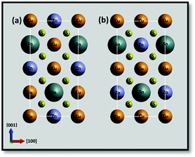
Density functional theory (DFT) calculations have examined the formation energies for various intrinsic point defects including vacancies and antisite defects on the Cu, Zn and Sn sites in the lowest energy kesterite structure shown in Fig. 1(a).5 These confirm that Cu/Zn disorder, which has been widely postulated by neutron diffraction studies,6 photoluminescence7,8 and X-ray diffraction,9 has a relatively low energy barrier. CuZn and ZnCu antisite defects should be shallow acceptors and donors respectively, leading to electrostatic potential fluctuations and local bandgap fluctuations where their distributions are non-isotropic. Using ab initio calculations, Scragg et al. have proposed that Cu/Zn disorder alone can account for the band gap variations and reductions in CZTS cell voltages observed experimentally.10 In addition CuZn and ZnCu antisite defects, as well as deeper levels due to Sn-related antisite defects, can potentially act as carrier traps and recombination centres leading to corresponding reductions in current and carrier lifetimes.
Although intrinsic defects are therefore likely to be an important factor limiting CZTS cell performance, their detection has been mostly confined to bulk techniques. Moreover, recent studies suggest that the surface stoichiometry, and thus the likelihood of intrinsic defects, can differ significantly from the bulk.11 It would therefore be highly desirable to get spatially resolved information on intrinsic defects. Transmission electron microscopy (TEM) can provide direct information on defects at high spatial resolution. Most TEM studies have concentrated on imaging extended defects including dislocations and twins by standard diffraction contrast methods, i.e. bright and dark field imaging.12 Mendis et al. have employed high spatial resolution electron energy loss spectroscopy (EELS) in a scanning transmission electron microscopy (STEM) in order to map the chemical content of individual atom columns in the 010 projection of CZTS (schematically shown in Fig. 1), providing direct evidence for Cu/Zn disorder.13
In this paper we throw new light on antisite defects present in CZTS nanocrystals, obtained by hot-injection synthesis,14 using high spatial resolution TEM and STEM methods. By using STEM to examine CZTS grains in the 010 orientation, we show evidence for high densities of antisite domain boundaries (ADBs). These boundaries are of several types, representing disorder on the Cu, Zn or Sn sites, with some boundaries effecting local changes in stoichiometry. It is also shown that there are regions within a few nanometres of the crystal surface with a marked increase in cation disorder, suggesting a model in which ADBs form following nucleation and subsequent coalescence of regions of local cation ordering. It is also shown that these defects can be examined in thicker regions of crystal by dark field imaging using reflections sensitive to the cation ordering. The paper explains the structure of the defects present, and discusses their wider significance.
CZTS nanoparticles were prepared by hot-injection in oleylamine following the protocol described in the ESI.†![[thin space (1/6-em)]](https://www.rsc.org/images/entities/char_2009.gif) 12,14 The nanoparticles were precipitated by adding a mixture of toluene and isopropanol, followed by centrifugation which, after several repetitions, allowed excess quantities of oleylamine. Particles in the range of 200 nm were obtained by annealing the CZTS nanoparticles in vacuum (see Fig. S1†). Previous studies employing selected area electron diffraction and convergent beam electron diffraction confirm that this methodology leads to sub-micron particles with a kesterite or stannite structure.12 SEM/EDX (Fig. S2†) and Raman spectra (Fig. S3†) are also consistent with high phase purity CZTS particles upon vacuum thermal annealing.
12,14 The nanoparticles were precipitated by adding a mixture of toluene and isopropanol, followed by centrifugation which, after several repetitions, allowed excess quantities of oleylamine. Particles in the range of 200 nm were obtained by annealing the CZTS nanoparticles in vacuum (see Fig. S1†). Previous studies employing selected area electron diffraction and convergent beam electron diffraction confirm that this methodology leads to sub-micron particles with a kesterite or stannite structure.12 SEM/EDX (Fig. S2†) and Raman spectra (Fig. S3†) are also consistent with high phase purity CZTS particles upon vacuum thermal annealing.
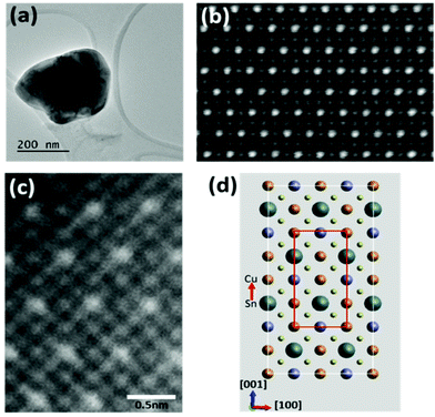
High resolution imaging studies were carried out on isolated individual crystals with thin edges overlapping holes in the carbon support film (Fig. 2(a)), and oriented to the exact [010] zone axis using Kikuchi bands seen in thicker regions. As illustrated in Fig. 1(a), the expected kesterite structure in this orientation consists of end-on columns of atoms each with a single atom species: Cu, Zn, Sn or S. The slightly higher energy stannite structure (Fig. 1(b)) differs from kesterite only in the arrangement of the Cu and Zn columns. Fig. 2(b) shows that the individual atom columns can be seen in high angle annular dark field (HAADF) images taken from a thin edge. The images were formed in STEM mode by scanning a focused probe (0.1 nm) across the sample and recording the high angle, mostly thermal diffuse, scattering on an annular detector. As the HAADF signal from the individual atom columns, to a good approximation, increases with the atomic number Z, these Z-contrast images15 show the brightest spots for the Sn columns (Z = 50) and weakest spots for the S columns (Z = 16). The contrast for the Cu (Z = 29) and Zn (Z = 30) columns is similar. The image in Fig. 2(c) shows contrast from all the atomic columns (Cu, Zn, Sn and S) as represented by the expanded unit cell shown in Fig. 2(d). The approximately hexagonal arrangement of the bright Sn columns can be seen in the schematic where the Sn atom columns are shown by larger discs compared to those for the other atom species. The S columns are represented by smaller discs to correspond to their weaker HAADF contrast, whereas columns with Cu and Zn atoms are given equal disc size to correspond with their close atomic numbers and HAADF contrast. In Fig. 2(b), and in some of the later images shown in the paper, the contrast levels are such that only the Sn, Cu and Zn columns show significant contrast.
The inability to distinguish Cu and Zn columns in HAADF images means that it is not possible using this technique alone to distinguish the kesterite and stannite structures. However, the structure was confirmed directly as kesterite by EDX mapping at atomic resolution, details of which will be reported elsewhere.
In the HAADF images in Fig. 3, there are boundaries across which there is a relative displacement of the brighter Sn columns. These fall into one of two types. Fig. 3(a) shows an apparently edge-on boundary with a trace (delineated) which is parallel to [100]. The boundary plane is thus (001). On the upper side of the boundary (grain I), the projected displacement is ½[100] compared to the crystal on the lower side (grain II) such that, assuming a kesterite structure, the Sn columns in grain I occupy what would otherwise be Cu columns for grain II. The structure is illustrated schematically for clarity. To minimise structural disorder, we expect that the grains have an additional relative displacement of ½[010] along the beam direction such that the total displacement is a cation–cation vector. The total fault displacement of R = ½[110] represents a pure shear if the boundary lies exactly on the (001) plane. The boundary should be considered as an antisite domain boundary, since the displacement translates cations from grain II into antisite positions for grain I. There is ambiguity as to whether the Cu/Zn plane in Fig. 3(a) belongs to grain I or II, as the image is insensitive to a Cu–Zn reversal, but, whichever it is, the boundary is typified by a complete antisite plane, i.e. a plane in which all the Cu and Zn atoms become ZnCu and CuZn antisite defects.
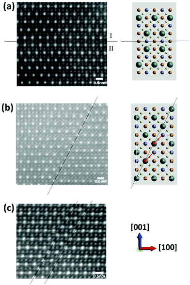 | ||
| Fig. 3 Atomic resolution HAADF images of antisite domain boundaries (ADBs) showing fault displacement of ½[110] (a), −¼[201] (b) and −½[201] (c). | ||
Fig. 3(b) shows a different type of boundary across which the [100] rows of Sn atom columns show a component of displacement in the [001] direction, i.e. ¼[001]. The boundary is again near edge-on but with a trace parallel to [101], with reference to the schematic of the unit cell. The projected relative displacement of the grains across the boundary plane is −¼[201], such that the Sn columns in the grain on the right move by the arrowed vector. Since the displacement vector is also a cation–cation vector, we expect no additional displacement along the viewing direction. In the schematic shown, the Sn atom columns replace Cu atom columns. However, as the images are insensitive to the difference between the Cu and Zn columns, the unit cell could be rotated by 180° about the [010] axis, such that the Sn–Cu vector shown in Fig. 2 points down and not up. In this case the Sn atom columns replace Zn atom columns. As the displacement vector is not parallel to the boundary plane, the displacement corresponds to the removal of material. The material loss could involve a plane of Cu atoms and a parallel plane of S atoms in the diagram shown, or planes of Zn and S atoms. The former should lead to a net positive charge, since equal numbers of Cu+ and S2− have been removed. In the case of ADBs involving the removal of Zn2+ and S2− atoms, these defects are likely to be neutral, although they could potentially be charged given the multi-valent nature of Sn. The boundary itself contains a plane of antisite defects, SnCu or SnZn with respect to the grain on the left. Fig. 3(c) shows another example of the structure in Fig. 3(b), where a second parallel equivalent fault brings the [100] rows of Sn atoms back into apparent registry, albeit such that the total displacement for the two faults is −½[201], not a complete lattice vector.
The boundaries in Fig. 3 are all antisite domain boundaries. For clarity, we have shown boundaries near edge-on, but it is clear that many boundaries are significantly inclined, such that the adjacent domains overlap. An example of this can be seen in Fig. 4 in the region labelled A. In Fig. 4 we also see a very thin region B near the crystal edge where a different structure is apparent. In this case there is no clear evidence for cation ordering, or indeed the overlap of ordered crystals, since all the cation columns show roughly equal intensity. There is no sharp boundary between ordered and disordered regions, with ordering becoming progressively more apparent as the crystal thickness increases.
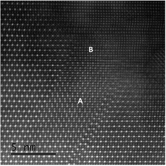 | ||
| Fig. 4 HAADF image illustrating regions near CZTS nanocrystal edge. Region A corresponds to inclined boundaries, while region B shows no apparent cation ordering. | ||
It is thus clear that the antisite domain boundaries can have a variety of orientations with boundaries near edge-on, inclined or possibly perpendicular to the viewing direction. From the crystallographic point of view, such faults can all be described by fault displacement vectors which connect cation columns. If we ignore cation ordering altogether, all the faults seen in Fig. 3 and 4 have displacements R representing ½<011> lattice spacings in the basic face-centred cubic (f.c.c.) unit cell from which the kesterite cell can be derived (where c is halved, and we ignore the tetragonal distortion produced by cation ordering). In terms of the f.c.c. unit cell, the kesterite cell can be seen as a superlattice structure. This implies that antisite boundaries should be invisible in dark (or bright) field images taken in the major reflections g associated with the f.c.c. cell, which would give g·R integer or zero values (the condition for fault invisibility) and potentially visible in the weaker “superlattice” reflections gs associated with cation ordering, in the case where gs·R is non-integer (note that gs·R can also be zero, or integer in the case of a closely spaced double fault as in Fig. 3(c)).
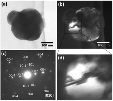
In Fig. 5, we make use of this fact to detect ADBs using a dark field image taken in the superlattice reflection g = 002, as confirmed by selected area electron diffraction (Fig. 5(c)). Switching from bright field (Fig. 5(a)) to dark field (Fig. 5(b)), sharp changes in contrast can be revealed, with some regions showing oscillatory fringe contrast indicative of inclined stacking faults (which are magnified in Fig. 5(d)). This is consistent with the presence of ADBs; for example, boundaries of type II with R = ¼[201] give g·R = ½ when g = 002 although a series of images taken in different superlattice reflections would be required to make an unambiguous assignment. It is also apparent that some faults must terminate within the bulk crystal. Such a termination must be seen as a bounding dislocation whose displacement b = R. In contrast to the ADB faults, such bounding dislocations should be visible in images taken in the major reflections g associated with the f.c.c. cell when g·R takes integer (non-zero) values.
The results here demonstrate clearly that CZTS crystals have antisite domain boundaries which can be directly studied by atomic resolution imaging. The results from a series of HAADF images over extended areas suggest that these boundaries can be present at very high densities, typically spaced 5–20 nm apart. Assuming an average spacing of 10 nm, this corresponds to 0.1 antisite pairs per unit cell on the premise that each boundary contains a single plane of atoms in antisite positions, or 3 × 10²⁰ antisite pairs cm−3. This compares with estimates of up to 0.8 Cu/Zn antisite pairs per unit cell (depending on the thermal history) based on a range of neutron diffraction and optical measurements,10 implying that the number of defect pairs in ADBs is likely to be less than that from random fluctuations. However, whether antisite pairs in ADBs have a greater effect on electronic properties than an equivalent number of isolated antisite pairs is not clear. It is likely that the boundaries of type I are relatively benign as the boundaries have no overall change in stoichiometry, and should be charged neutral. It is also possible that boundaries of this type may be annealed out, as this requires a simple slip process. On the other hand, boundaries of type II are different in that they describe a change in the stoichiometry. As noted earlier, there is an ambiguity as to whether type II boundaries represent removal of planes of Cu and S, as in the schematic in Fig. 3, or removal of planes of Zn and S. In either case, type II boundaries should be relatively high energy boundaries as both SnCu and SnZn defects have high formation energies (in the region of 6 eV and 4 eV, respectively).16 Moreover, Sn antisite defects are related to deep energy levels which can have a profound effect on carrier mobility and lifetime. If, as in Fig. 3, planes of Cu and S have been removed, these boundaries should also contain a net positive charge. This should result in local potential fluctuations which manifest themselves as band tails. These tails have been linked to low open circuit voltage which limit the device efficiency. The elimination of type II ADBs is also unlikely through annealing, as the addition of material is needed to balance the stoichiometry. Thus, type II ADBs may be a limit on the extent to which annealing can be used to improve the solar cell performance of CZTS.
Observations of the very thin edges, as in region B of Fig. 4, show a reduction in contrast between the Sn and the Cu/Zn columns. This could indicate preferential loss of Sn near the crystal surfaces, compared with Cu or Zn, perhaps during annealing at 550 °C. However, preliminary EDX mapping across the crystal edges (Fig. S4†) has shown no evidence for such a reduction of Sn concentration at the crystal edges. This suggests, alternatively, that there is increasing disorder on the cation sites towards the crystal surfaces, i.e. with Sn, Cu and Zn spread more evenly between the cation columns. Fig. 4 suggests that the underlying cubic lattice in this disordered region is continuous with the more ordered structure seen in the adjacent thicker regions. Antisite domain boundaries could therefore be seen as a consequence of independent nucleation, followed by coalescence, of different ordered regions within the disordered crystal, i.e. a sintering process with small grains having relative displacements given by a lattice vector for the cubic cell but not for the kesterite cell. Alternatively, it could be that the disordered material acts as a reservoir for growth of the underlying ordered material, such that the growth of previously nucleated ADBs is perpetuated. The dark field observations shed some light on this, showing that ADBs extend over distances >100 nm in some cases (Fig. 5b is an example), suggesting that the latter nucleation and propagation process is more likely. As some antisite boundaries describe changes in stoichiometry, e.g. the boundaries seen in Fig. 3(b) and (c) represent removal of S and Cu planes, it is possible that antisite boundary formation is driven by changes in stoichiometry at the surface. However, whether stoichiometry is a factor remains to be determined.
Acknowledgements
The financial support by the EPSRC Centre for Doctoral the BCFN and Taibah University (Saudi Arabia) is acknowledged. DJF is also grateful to the EPSRC for funding through the PVTEAM programme (EP/L017792/1) and to the Institute of Advanced Studies of the University of Bristol for support through the University Research Fellowship 2015. The authors are grateful for the use of the South of England Analytical Electron Microscope, EPSRC grant EP/K040375/1, and acknowledge the fruitful discussions with Dr Devendra Tiwari (University of Bristol).References
- T. Kato, H. Hiroi, N. Sakai, S. Muraoka and H. Sugimoto, 27th Eur. Photovolt. Sol. Energy Conf. Exhib., 2012, 2236–2239.
- D. Mitzi, O. Gunwan, T. Todorov and D. Barkhouse, Philos. Trans. R. Soc. London, 2013, 371, 20110432 CrossRef PubMed.
- H. Katagiri, K. Jimbo, M. Tahara, H. Araki and K. Oishi, Mater. Res. Soc. Symp. Proc., 2009, 1165, 1165-M04 Search PubMed.
- A. Nagaoka, H. Miyake, T. Taniyama and K. Yoshino, Appl. Phys. Lett., 2013, 103, 112107 CrossRef.
- S. Shen, A. Walsh, X. Gong and S. Wei, Adv. Mater., 2013, 25(11), 1522–1539 CrossRef PubMed.
- S. Schorr, H. J. Hoebler and M. Tovar, Eur. J. Mineral., 2007, 19, 65–73 CrossRef CAS.
- T. Gokmen, O. Gunawan, T. Todorov and D. Mitzi, Appl. Phys. Lett., 2013, 103, 103506 CrossRef.
- T. Gershon, B. Shin, N. Bojarczuk, T. Gokmen, S. Lu and S. Guha, J. Appl. Phys., 2013, 114, 154905 CrossRef.
- T. Washio, H. Nozaki, T. Fukano, T. Motohiro, K. Jimbo and H. Katagiri, J. Appl. Phys., 2011, 110(7), 074511 CrossRef.
- J. Scragg, J. Larsen, M. Kumar, C. Persson, J. Sendler, S. Siebentritt and C. Platzer Björkman, Phys. Status Solidi B, 2015, 253(2), 247–254 CrossRef.
- R. Haight, X. Shao, W. Wang and D. Mitzi, Appl. Phys. Lett., 2014, 104, 033902 CrossRef.
- N. Kattan, B. Hou, D. Fermín and D. Cherns, Appl. Mater. Today, 2015, 1, 52–59 CrossRef.
- B. Mendis, M. Shannon, M. Goodman, J. Major, R. Claridge, D. Halliday and K. Durose, Prog. Photovoltaics, 2014, 22, 24–34 CAS.
- B. Hou, D. Benito-Alifonso, N. Kattan, D. Cherns, M. Galan and D. Fermín, Chem. – Eur. J., 2013, 19, 15847–15851 CrossRef CAS PubMed.
- S. J. Pennycook and D. E. Jesson, Phys. Rev. Lett., 1990, 64, 938–941 CrossRef CAS PubMed.
- S. Chen, J. Yang, X. Gong, A. Walsh and S. Wei, Phys. Rev. B: Condens. Matter, 2010, 81, 245204 CrossRef.
Footnote |
| † Electronic supplementary information (ESI) available: TEM image of CZTS particles after annealing, SEM/EDX and Raman spectra of CZTS particles and EDX mapping of particle edge. See DOI: 10.1039/c6nr04185j |
| This journal is © The Royal Society of Chemistry 2016 |

