
 Open Access Article
 This Open Access Article is licensed under a
 Creative Commons Attribution 3.0 Unported Licence
Towards an optimal contact metal for CNTFETs†
Artem
Fediai
*ab,
Dmitry A.
Ryndyk
ab,
Gotthard
Seifert
bcd,
Sven
Mothes
be,
Martin
Claus
be,
Michael
Schröter
be and
Gianaurelio
Cuniberti
abd
aInstitute for Materials Science and Max Bergmann Center of Biomaterials, 01062 Dresden, Germany. E-mail: artem.fediai@nano.tu-dresden.de
bCenter for Advancing Electronics Dresden, TU Dresden, 01062 Dresden, Germany
cTheoretical Chemistry, TU Dresden, 01062 Dresden, Germany
dDresden Center for Computational Materials Science (DCMS), TU Dresden, 01062 Dresden, Germany
eChair for Electron Devices and Integrated Circuits, TU Dresden, 01062 Dresden, Germany
First published on 1st April 2016
Abstract
Downscaling of the contact length Lc of a side-contacted carbon nanotube field-effect transistor (CNTFET) is challenging because of the rapidly increasing contact resistance as Lc falls below 20–50 nm. If in agreement with existing experimental results, theoretical work might answer the question, which metals yield the lowest CNT–metal contact resistance and what physical mechanisms govern the geometry dependence of the contact resistance. However, at the scale of 10 nm, parameter-free models of electron transport become computationally prohibitively expensive. In our work we used a dedicated combination of the Green function formalism and density functional theory to perform an overall ab initio simulation of extended CNT–metal contacts of an arbitrary length (including infinite), a previously not achievable level of simulations. We provide a systematic and comprehensive discussion of metal–CNT contact properties as a function of the metal type and the contact length. We have found and been able to explain very uncommon relations between chemical, physical and electrical properties observed in CNT–metal contacts. The calculated electrical characteristics are in reasonable quantitative agreement and exhibit similar trends as the latest experimental data in terms of: (i) contact resistance for Lc = ∞, (ii) scaling of contact resistance Rc(Lc); (iii) metal-defined polarity of a CNTFET. Our results can guide technology development and contact material selection for downscaling the length of side-contacts below 10 nm.
1. Introduction
Carbon nanotube field-effect transistors (CNTFETs) have been considered as one of the major contenders for replacing digital Si-CMOS technology beyond the 7 nm node and for complementing highly linear analogue applications.1,2 The high expectations from the CNTFET technology have arisen mainly due to the unique intrinsic properties of single wall CNTs.3 One major obstacle to find access to these properties in practical electronic applications is the contact. Thus, major achievements in the fabrication of CNTFETs allowing access to the intrinsic CNT properties are related to the progress in CNT–metal contact fabrication. For instance, Javey et al. have made a breakthrough by demonstrating the first ohmic contact to a CNT,4 and Franklin and Chen have shown promising scaling abilities when decreasing the length of a CNT–metal contact.5 Finally, the challenges in reaching small contact resistance for sub-10 nm contacts were reported in ref. 6, which calls for appropriate theoretical support.Depending on the contact geometry, end- and side-bonded CNT–metal contacts can be distinguished. Throughout this paper we restrict ourselves to the practically relevant sub-class of side-contacts, namely when the CNT is completely wrapped by the deposited metal, which we refer to as embedded contact. The embedded contact scheme has driven the progress of CNTFET technology over the last decade; in particular, it has been shown to provide the lowest contact resistance.6
In line with experimental studies, a lot of theoretical ab initio studies were carried out which aimed at understanding the electrical properties of the contact (mainly, resistance) depending on the contact metal. Most of those studies, however, were devoted to the end-contact geometry,7–10 which is not the subject of this paper.
Embedded contacts have been considered in several theoretical studies. For instance, Vitale et al. have defined a Schottky barrier between an (8,0) CNT, with one unit cell embedded into Al and Pd.11 Zhu and Kaxiras have analysed the charge transfer and the density of states (DOS) in two periods of CNT embedded into Pd.12 The projected DOS as a function of distance and transmission coefficient were calculated in ref. 13 by Palacios et al. for an (8,0) short CNT embedded from left and right by one layer into Au and Pd electrodes using the Green function method. In ref. 14, the Green function formalism was used to calculate the transmission coefficient for a similar structure, where only three CNT unit cells are embedded into the electrode.14
None of the summarized references above takes into account (1) the sufficiently long embedded CNT part inside the metal and (2) the transition region between the embedded and uncoated CNT part, which play an essential role for practical embedded CNT–metal contacts. Although ref. 11–14 provide new scientific information on CNT–metal interaction, they do not allow for establishing a link between the contact metal and electrical properties of the embedded CNT–metal contact.
Although the non-equilibrium Green function method (NEGF) with Kohn–Sham Hamiltonian (hereinafter, DFT + NEGF method) is the most rigorous form of the possible DFT-based approaches, ref. 13 and 14 with simulated contact lengths of only a few Angstroms cannot explain the experimentally observed electrical properties of embedded CNT–metal contacts, which exhibit a strong contact length dependence of the contact resistance for contact lengths beyond 10 nm.6
On the other hand, there exists another trajectory of research studies, established by Knoch et al.15 and Nemec et al.16,17 and used in ref. 18 and 19. This approach treats an embedded CNT–metal contact explicitly as an extended contact. It predicts low-ohmic CNT–metal contacts to be formed for metals weakly interacting with CNTs, and an increasing contact resistance with decreasing contact length, which agrees qualitatively with the contact resistance scaling reported in ref. 5 and 6. Although Nemec et al. utilised both NEGF and DFT in ref. 16 and 17, it is not yet a rigorous combination of the NEGF and DFT, which was also not applicable to any metal. The reason why this approach was not upgraded to the quantitative level is that one needs to simulate extremely long (in terms of DFT calculations) metallic electrodes (up to ≈100 nm) and connect them appropriately to the tube. This is an infeasible task due to the enormous numerical resources required, if one treats quantum transport without any special methods. On the other hand, numerically efficient implementations of NEGF + DFT methods are only available for quasi-1D contacts, and are unsustainable when treating side-bonded contacts, in which there exists one more relevant space direction.
Recently, however, a rigorous NEGF + DFT approach for simulating side CNT–metal contacts has been developed.20 It utilizes explicitly the concept of the extended contact,16 but in its core it is a rigorous DFT + NEGF method dedicated to side contacts. It exceeds beyond previous reports11–14,17 in several regards, in particular: (1) both the extra-long embedded part of the contact and the transition region at the interface between the coated and uncoated tube part are taken into account; (2) it makes the simulation of CNT–metal contacts numerically feasible even for very long contact lengths; (3) it is applicable to any contact material, i.e. the method is universal unlike that in ref. 16; (4) it is able to predict the CNT doping and other changes of the CNT electronic structure covered by the metal.
In this work we have extended an approach20 towards non-zero bias in order to calculate the contact resistance of CNTFETs for a set of different contact metals, which represent a wide spectrum of different carbon–metal bonding strengths and electro-negativity. We have discovered the prerequisites for realizing a low-ohmic contact depending on the contact length. For very long contacts with weakly-interacting metals we have found that the contact resistance does not depend much on a metal work function and tends towards the quantum resistance  (divided by a number of conducting modes m). However, the different electrostatic barrier between the coated and uncoated tube part is a reason why the contact resistances are not precisely equal to R0/m. Only for very strong interactions, which are typical for chemisorbed metals, long CNT–metal contacts could have high resistance due to (1) the Fermi level pinning at the interface between the coated and uncoated tube part, and (2) a significant modification of the electronic structure of the embedded tube.
The dependence of the contact resistance on contact length scaling is much more diverse. Weakly interacting metals could have either poor scaling behaviour (Rc grows steeply for Lc < 50 nm) or good scaling behaviour (Rc is almost constant down to 10 nm). On the other hand, the contact resistance of the chemisorbed metals does not depend on length down to 5–10 Å. Besides, it starts to oscillate when approaching the sub-10 nm limit.
We compared our calculations with the experimental data of Rc![[thin space (1/6-em)]](https://www.rsc.org/images/entities/char_2009.gif) 6 and obtained semi-quantitative agreement for most of the metals.
6 and obtained semi-quantitative agreement for most of the metals.
2. Results
2.1 General choice of the simulated systems and approximations
We have calculated contact resistances of carbon-nanotube transistors with 40 nm channel length (Lch) made of a (16,0) semiconducting CNT and embedded contact lengths Lc ∈ [0.45 nm; −∞) (Fig. 1(a)). The atomistic structures considered here are as close as possible to fabricated CNTFETs (see Table 1), for which the contact resistance Rc has been measured for both long and sub-100 nm contacts.5,6,21 | ||
| Fig. 1 Geometry of the embedded contact (a) and an order of the decimation shown for the toy model of the extended CNT–metal contact (b, c, d). | ||
2.2 Brief method description
According to recent experiments,6,21 the electric current enters from the metallic contact into the tube over a width of up to 100 nm. Standard DFT + NEGF methods are intended to treat quasi-one-dimensional atomistic systems with a localised current inflow, which would require performing explicit DFT calculation of an entire 100 nm metal–CNT contact, which is numerically intractable. We overcome this challenge by utilizing an adaptive NEGF + DFT method described in detail in ref. 20, which is provided for an adaptive treatment of contacts with a distributed current inflow. Like in the usual NEGF + DFT method,22 the whole system is decomposed into three parts, the “left” (L) and “right” (R) leads (which include embedded tube parts and metallic electrodes) and the “scattering” (S) region in between (uncoated tube portion). However, in contrast to the conventional implementation, we use a two-stage procedure of the decimation of the leads’ Hamiltonians as illustrated in Fig. 1:(i) we substitute the Kohn–Sham Hamiltonian of the initial system (Fig. 1a and b) by the Hamiltonian of the carbon subsystem H only and the self-energies of the metal electrodes  (Fig. 1c). At this stage, H still includes both covered and uncovered tube portions.
(ii) We decimate an effective Hamiltonian of the embedded CNT to obtain the self-energies of the contacts (Fig. 1d).
After the first stage (Fig. 1c), the effective Hamiltonian of the whole system can be summarized as:
 | (1) |
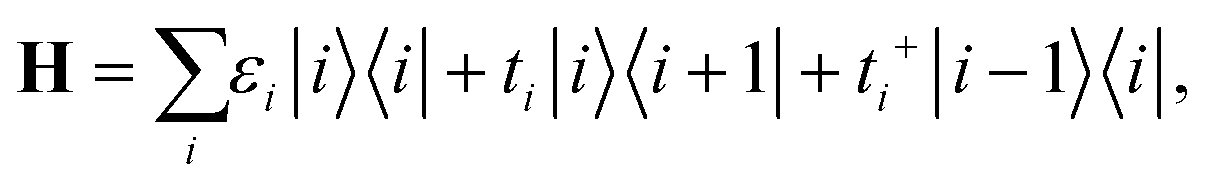
Note that in contrast to the standard NEGF technique,23 the Hamiltonian in eqn (1) is an effective rather than the actual one (it is complex and energy-dependent). Both the Hamiltonian of the carbon subsystem H and the self-energies of the leads  are assumed to be tightly bound (the length of carbon–carbon interaction is assumed to be zero starting from the forth nearest neighbour). The only non-zero elements of the self-energy
  are:
are:  , and
, and  , where rC, r′C, r′′C and rC(3) stand for the coordinate of a given carbon atom and its three nearest neighbours (|rC − r′C| < |rC − r′′C|).
As a further approximation we replace the actual tube by the corresponding flat nano-ribbon (NR) subjected to cyclic boundary conditions (CBC) and the metal slab below. This approximation is well justified for the relevant range of CNT diameters considered in this paper, as it has been shown in ref. 24 and 25. Our treatment requires also a common periodicity of the metal slab and the honeycomb lattice of carbon. This can be realized by the proper orientation of the carbon layer with respect to the metal surface as it was realized already for metal–graphene contacts24,25 and by the corresponding small stretching/compression of the metal lattice (<3% for all metals except Rh; that was stretched by 5%). We have checked that the density-of-states (DOS), work function and the band structure around the Fermi energy of the metals have not changed significantly by such extension/compression.
 | (2a) |
 | (2b) |
In eqn (2), |i〉 includes all orbitals of the i-th CNT unit cell (64 × 4 orbitals for (16,0) CNT taken in SZV-basis); “i ∈ L(R)” means that a sum goes thorough all CNT unit cells within the left (right) embedded tube part. εi and ti are the on-site matrix of the CNT unit cell and the hopping matrix between two adjacent CNT unit cells, respectively, whereas σε and σt are the corresponding elements of the self-energy. Note that we have preserved the tight-binding form of both Hamiltonian (eqn (2a)) and self-energy (eqn (2b)), which is a prerequisite for using the standard NEGF formalism (which is described, for example, in ref. 23).
The electric current has been calculated according to the Landauer formula:

f s(E) = fF(E), fd(E) = fF(E + eVds), where fF(E) is a Fermi function; e and h stand for elementary charge and the Planck's constant, respectively. Both the transmission coefficient T and the current Ids are functions of Vds, Vgs and Lc.
The density of states at the i-th CNT-unit cell has been calculated according to the formula:

Density of states inside the embedded CNT part has been calculated for an auxiliary system, whose periodic tight-binding effective Hamiltonian was built out of on-site h∞ and hopping t∞ elements of the deeply embedded tube (4-th CNT unit cell away from a contact edge) and the corresponding self-energies (σε, σt):
 | (3) |
We used a highly-converged numerical30 method to find the bulk Green's function of this periodic tight-binding system, gRinside, and then the following formula was used:

The spectral function of the embedded CNT part has been computed for the same auxiliary system (eqn (3)) as follows:
| A(k,E) = iTr[(gR(k,E) − gA(k,E))s(k)], |
Sharp peaks of A(k,E), for a given k correspond to the weak interaction; smeared peaks correspond to the intermediate interaction, and strongly-smeared peaks correspond to the strong interaction. The ultimate case, when A(k,E) → ∞ for some (k,E), corresponds to the absence of an electrical interaction. In this case, coordinates of the poles are defined by the dispersion relation E(k) in the (k,E)-plane.
The dispersion relation E(k) for each CNT unit cell has been defined as described in ref. 20. The band edges Ec and Ev have then been extracted out of it and used to plot the corresponding band profiles.
2.3 Selection of the metals and metal–CNT separation
Ten contact metals were explored so as to represent (a) metals with different work functions, and (b) metals with different carbon–metal bonding strengths – from chemisorption to physisorption (see Table 2).| Element | Al | Sc | Ti | Cr | Ni | Cu | Rh | Pd | Pt | Au |
|---|---|---|---|---|---|---|---|---|---|---|
| d Me–C is a metal–carbon separation being used throughout this work; WMe is the metal's work function calculated by DFT for actual metal interfaces employed in this work. Eb is the binding energy per carbon atom in metal–graphene complexes as calculated in ref. 33. | ||||||||||
| d Me–C, Å | 3.80 | 4.00 | 2.08 | 3.75 | 2.08 | 3.70 | 3.70 | 3.75 | 3.75 | 3.57 |
| W Me, eV | 4.10 | 3.53 | 4.46 | 4.04 | 5.17 | 4.85 | 5.23 | 5.09 | 5.68 | 5.05 |
| E b, meV per C atom | −42 | n.d. | −46 | n.d. | −133 | −30 | n.d. | −89 | −46 | −37 |
One of the principal issues in atomistic simulations of CNT–metal contacts is the arrangement of the carbon and metal atoms near the metal–CNT interface. Owing to the usage of the “rolled-out” CNT, in choosing the carbon–metal separation dMe–C, we were guided by the distances in metal–graphene systems, which have been extensively investigated.31–34 Different DFT studies give a large variety in graphene–metal separation, mainly due to the usage of different van der Waals functionals and different DFT approximations. Especially for Pd the variation is very large (in ref. 31 it was reported dPd–C = 2.3 Å, whereas according to ref. 35 an upper limit of this distance is 4.04 Å). For the rest of the metals it is usually agreed that Ni and Ti have a distance close to the sum of covalent radii, whereas dMe–C of other metals, which are considered here, is close to the sum of van der Waals radii of the metal and carbon atoms. Not to rely on a specific van der Waals interaction model, for physisorbed metals (to which we ascribe Al, Sc, Cr, Cu, Pd, Pt and Au) we used a sum of van der Waals distances (as calculated in ref. 36); for Ni and Ti the distance 2.08 Å was applied, which is close to those computed in ref. 34 and 35. For Au we have used dMe–C = 3.57 Å, which is 0.23 Å smaller than the sum of the van der Waals radii – for reasons described below. The influence of the metal–carbon distance on the electrical characteristics of CNT–metal contacts will be considered in more detail elsewhere.
2.4 Extraction of the contact resistance
The contact resistance has been extracted in a way close to that used in ref. 6. We assume that the external drain–source voltage Vds and gate–source voltage Vgs modify the system's Hamiltonian (eqn (1)) as follows: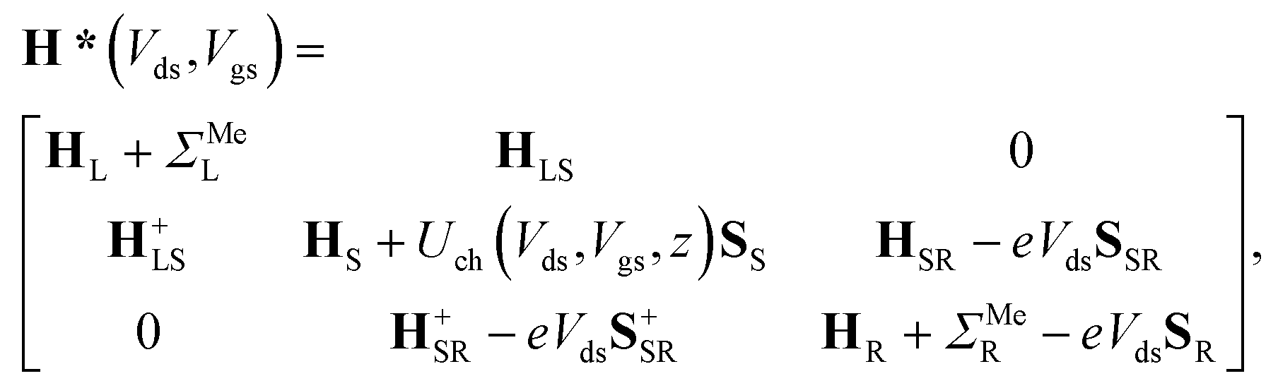 | (4) |
 | (5) |
The contact resistance Rc has been defined as 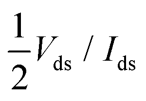 (we use the same definition of Rc as in ref. 6, and do not discuss the physical aspects of this quantity). For all of the contact metals, Rc has been calculated for an overdrive voltage of Vgs − Vth = ±0.5 V and for Vds = ±0.025 V (sign “+” for n- and “−” for p-type contacts), which is the same condition as in the experimental studies (ref. 6 and 21) we intend to compare our results with.
The calculated contact resistances Rc of infinitely long contacts for each of the contact metals are shown in Fig. 2, accompanied by the experimental data taken from ref. 6. Three contact metals can be distinguished which remain high-ohmic even for infinitely long contacts: Al, Ti and Ni. Contacts made of Au, Cu, Pd, Cr, Rh have a resistance of about 12 kΩ, whereas Pt and Sc contacts provide a contact resistance of less than 10 kΩ.
 | ||
| Fig. 2 Contact resistance Rc of the 40 nm channel CNTFETs with very long (infinite) contacts. Experimental data are taken from ref. 6. Both experimental and theoretical data have been defined under the same bias conditions. | ||
Fig. 3 shows the contact length dependence of the contact resistance for different metals. We can distinguish between high-ohmic contacts (Al, Ti, Ni), whose resistance depends weakly on the contact length (Fig. 3a), low-ohmic contacts (Cu, Rh, Sc) whose resistance depends weakly on the contact length (Fig. 3b), and low-ohmic contacts (Cr, Pd, Pt, Au), whose contact resistance depends strongly on the contact length (Fig. 3c).
 | ||
| Fig. 3 Scaling behaviour of the contact resistance Rc(Lc) calculated for different metals: (a) Al, Ti and Ni, for which Rc is high and contact length dependence is weak; (b) Cu, Rh, Sc, for which Rc is low with a weak dependence on contact length (c) Cr, Pd, Pt and Au, for which Rc grows sharply when approaching the sub-10 nm range, but long contacts are low-ohmic. The oscillations observed are due to complicated quantum interference effects. | ||
Scaling of the contact resistance for Rh-, Au-, Pt- and Pd-contacts is shown in Fig. 4a and compared to the corresponding experimental data6 (Fig. 4b). The simulated scaling behaviour of Rc agrees qualitatively with experimental data. However, the experimental dependence on contact length is stronger for Rh, but weaker for Au, Pt and Pd. The magnitude of the calculated contact resistances spans a range of 7–12 kΩ per CNT, whereas the corresponding experimental values are within 5–10 kΩ per CNT. According to our simulations, the contact resistance of Ni and Ti-contacted CNTFETs is high, but contact length-independent down to 5–10 nm. In experiments, however, Rc of Ti- and Ni-contacts increases with decreasing Lc, which may be attributed to the increased impact of residual resists for shorter contact lengths6 and higher reactivity of Ti and Ni surfaces.
 | ||
| Fig. 4 Simulated contact resistance scaling (a) vs. experimental results (b) for Rh, Pd, Pt and Au contacts. The simulated data for Rh, Pd and Pt was plotted as is with the step of 0.426 nm (period of the CNT unit cell) with a black line and smoothed by thick color lines to show the trend of Rc(Lc) omitting oscillations. | ||
3. Discussion
We discuss for a series of different metals, ranging from those with a strong metal–carbon interaction to those with a very weak interaction, physical mechanisms, which govern the length and material dependence of the contact resistance. First we discuss the asymptotic behaviour (infinite contacts) and secondly, the scaling behaviour (finite contact length).3.1. Infinite contacts
 | ||
| Fig. 5 Electrical properties of the embedded tube part: spectral function A(E,k) (upper panel) and density of states projected on the carbon atoms of the embedded tube DOSinside(E) (lower panel) for Ti and Pt contacts, which represent strong and very weak electrical interactions, respectively. DOSinside(E) and A(E,k) are in eV−1 per C atom and per CNT unit cell (64 C atoms), respectively. | ||
The strong interaction described above is due to the high values of both the real and the imaginary part of the self-energies 〈rC|ΣMe|rC(i)〉, approaching 30 eV per carbon atom for Ni contact and 8 eV per carbon atom for Ti contact (see Fig. 6a–c). These large values of the self-energy should not be confused with the shift of the CNT bands, which is comparable to that in graphene.34,35 The former characterizes the effect of a metal on the embedded CNT; the latter characterizes the changes of a CNT subsystem due to the interaction with the metal.
 | ||
| Fig. 6 The most important matrix elements of the self-energy Σ between π orbitals: imaginary part (a) and real part (b) of the diagonal element, and real part of the self-energy between the two nearest carbon atoms (c). | ||
The calculated contact resistances Rc of Ti–CNT and Ni–CNT contacts are among the highest for all explored metals due to the combination of two factors. First, due to the large magnitude of self-energy elements, the transmission coefficient is suppressed already at zero bias (Fig. 7a). Second, due to the high interaction with the metal, the Fermi level of the uncoated tube part is pinned near the center of the band gap of the CNT (Fig. 8j and e). Since Ti and Ni contacts lead to a metallization of the coated tube part, both contacts can be approximately understood as conventional Schottky contacts between the metallized and the semiconducting tube. This simplified model, although, would not account for the contact resistance increment due to a metal–CNT interaction, which always plays a destructive role for the infinite extended contact transparency.
 | ||
| Fig. 7 Zero-bias transmission coefficient through a CNTFET with (a) Ni (represents chemisorbed metals) and (b) Sc (represents physisorbed metals) infinite contacts and 40 nm channels (coloured areas). Dashed lines show the transmission coefficient of the pristine tube. | ||
 | ||
| Fig. 8 Local density of states (LDOS) projected onto carbon orbitals along the 9 nm channel CNTFET and band edges (if defined) for the investigated metals. Vertical lines denote the edges of the contacts; the dashed horizontal line indicates the Fermi level. No bias has been applied. The colour bar shows the carbon LDOS in (eV−1) per C atom. | ||
To characterize bend bending between the covered and uncovered tube parts quantitatively, we introduce a quantity ϕSb which we refer to as the Schottky barrier defined as Ec − EF or EF − Ev (for n- or p-type contacts, respectively) in the channel at a distance 1 nm from the left contact, which is similar to the conventional Schottky barrier definition, if a covered CNT part is metallized. The height of corresponding Schottky barriers are shown in Fig. 9 for all metals.
 | ||
| Fig. 9 Dependence of the contact resistance for infinitely long contacts on the Schottky barrier height, ϕSb. ϕSb is defined as Ec − EF or EF − Ev (for n- or p-type contacts, respectively) in the channel at a distance of 1 nm from the left contact (note, that we call this quantity “Schottky barrier”, even though the embedded tube is not always metallized). | ||
It is easy to see, why weakly interacting metals do not change the band structure of the embedded CNT significantly by looking at the calculated self-energies as shown in Fig. 6. Even though the imaginary/real part of the self-energy 〈rC, π|Σ(E)|rC(i), π〉 varies over 3 orders of magnitude depending on the metal type (for instance, −Im〈rC, π|Σ(E)|rC, π〉 ∈ [10−1; 10−4]), the resulting contact resistances differ only by a factor of two for all weakly-interacting metals (Fig. 2). This is because −Im〈rC, π|Σ(E)|rC, π〉 and Re〈rC, π|Σ(E)|rC, π〉 are both negligible at the scale of the CNT band gap (Eg = 0.64 eV) and hopping element between the π orbitals of the nearest C atoms 〈rC, π|H|r′C, π〉 ≈ 2.7 eV; for Pd, Pt and Cr they are even less than the room temperature kT ≈ 0.025 eV (Fig. 6).
There is, however, one parameter, which varies strongly even for weakly interacting metals. This is the doping of the metal-coated tube part. Quantitatively we characterise doping by a difference between a Fermi level and the center of the band gap, ½(Ec + Ev) − EF. Whether the CNT is p- or n-doped depends on the work-function difference between a given metal and the CNT, WMe − WCNT, and on the strength of the CNT–metal interaction – much like in the case of graphene–metal contacts.31 We observe p-type doping for Pd and Pt contacts and n-type doping for Cr and Sc contacts, which agrees well with the work-function differences WMe − WCNT (see Fig. 10). Provided that WMe − WCNT differs significantly from zero (which is the case for Pd, Pt, Cr and Sc), CNTs can lose/acquire electrons causing EF penetration into the conduction (valence) band to provide strong n+ (p+) doping.
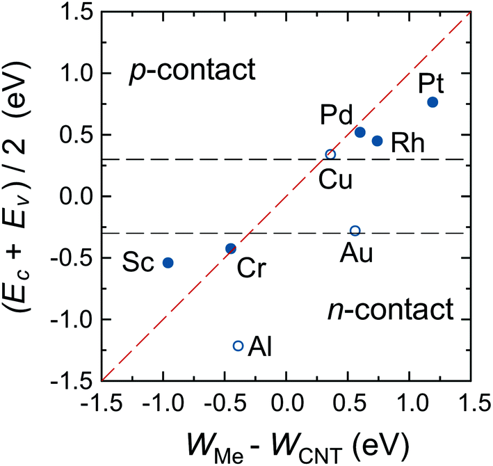 | ||
Fig. 10 Doping of the embedded tube depending on the difference between the CNT and metal work function. The red dashed line is  , which is similar to the Schottky–Mott rule. Horizontal lines represent the band edges (Ec and Ev) of a pristine tube, and are an eye-guide to distinguish between n- and p-type doping. Empty circles represent metals with a considerable real part of the self-energy. , which is similar to the Schottky–Mott rule. Horizontal lines represent the band edges (Ec and Ev) of a pristine tube, and are an eye-guide to distinguish between n- and p-type doping. Empty circles represent metals with a considerable real part of the self-energy. | ||
The shift of the Fermi level in the channel, which follows the same direction as in the contact, looks different compared to the pristine CNT, and we could naively expect large charge transfer similarly to the embedded tube part. This is not the case though. We have found that max(Ec − EF, EF − Ev) > 3kT for all four metals, which means that the recharge of a channel is negligible.
As a result, bend bending across the edge of a CNT–metal contact looks either like an n+–n (Fig. 8i and c) or p+–p junction (Fig. 8f and g). The transmission coefficient through a CNT embedded into a weakly interacting metal is very close to that of an intrinsic tube, apart from shifting relative to the Fermi level due to metal-induced doping. Zero transmission is observed for an energy range that corresponds to the band gap energies of either the covered or uncovered tube part (see Fig. 7b).
Important associated conclusions can be derived for very weakly interacting metals:
1. Electron transport in CNT–metal contacts can be described with a simple empirical model where the metal-coated CNT part and the metal contact is simply modelled as a doped CNT.39 The amount of doping can be determined from our ab initio simulations.
2. It is well-known that a small, but finite imaginary part is added to the energy in the numerical implementation of the NEGF; being smaller than kT, it yields insignificant changes of the system's electronic properties. For weakly interacting metals this small imaginary part arises naturally due to the weak interaction with a metal. Therefore, it is not necessary to calculate the metal's self-energy for simulating the electric transport in CNT–metal contacts, if a metal belongs to the weakly-interacting class.
Bend-bending and the presence of a small, but finite potential barrier between embedded and free CNT parts (see Fig. 9) are the reasons, why the contact resistance is not precisely equal to the quantum of resistance (divided by the number of conduction channels at the Fermi level).
In contrast to the weakly interacting metals, Au, Al and Cu lead to a considerable reconstruction of the embedded CNT's band structure due to the relatively large real part of the metal's self-energy Re〈rC, π|Σ(E)|rC(0,1), π〉, which is of an order of ±1 eV (see Fig. 6b and c). The element Re〈rC|Σ|rC〉 is added to the effective potential, which is already shifted due to CNT doping. Element Re〈rC, π|Σ|r′C, π〉 changes the hopping element between the π orbitals of the two nearest C atoms 〈rC, π|H|r′C, π〉 (which is equal to 2.7 eV for a pristine tube). This element is related to the band gap, the effective mass and other band structure parameters. Matrix elements, which correspond to more distant C atoms (e.g., larger |rC − rC(i)|) are much smaller, for instance, 〈rC|Σ|rC(3)〉 is of an order of ±0.1 eV.
Fig. 11 shows the spectral function A(E,k) (upper panel) and density of states (lower panel) of the tube embedded into Au, Al, Cu and Rh.
 | ||
| Fig. 11 Electrical properties of the embedded tube part: spectral function A(E,k) (upper panel) and density of states projected on carbon atoms of the embedded tube DOSC(E) (lower panel) for Cu, Al, Au and Rh contacts, which represent the intermediate electrical interaction. DOSC(E) and A(E,k) are in eV−1 per C atom and per CNT unit cell (64 C atoms), respectively. | ||
For Cu, the A(E,k) shows a strong interaction (like in the case of chemisorbed metals). However, the intrinsic CNT band structure is yet slightly visible (Fig. 11a). The projected density of states in the Cu–CNT system shows rehybridization: the DOS is distributed among s and p orbitals, and no signs of sp2 hybridization are observed.
In its turn, Al slightly spreads the CNT band gap (+0.1 eV), strongly shifting downwards and reconstructing the bands (changing the distances between van Hove singularities, etc. – Fig. 11b). The Al-coated CNT part is heavily doped and almost behaves as a metallized CNT. Unlike all other weakly-interacting metals, the channel of the CNT remains undoped leading to potential barriers for holes and electrons at the interface between the coated and uncoated tube part (Fig. 8b and 9). This enhances Rc of the CNT–Al contact.
The Au-contacted CNT is metallized mainly due to π orbitals. The matrix element Re〈rC, π|Σ|rC, π〉 = 0.57 eV, which adds up with an effective potential of the embedded CNT, shifts the bands of an embedded CNT upwards, so that the composite system resembles graphene with n-type doping, although the embedded CNT is itself p-type doped. It is noteworthy that the self-energy elements for Au contacts have unusual dependence on dAu–C: instead of a monotonous decreasing, it keeps increasing until dC–Au = 4.0 Å. For dC–Au = 3.8 Å, Rc of the Au contact reaches the highest magnitude. Out of 10 explored metals, Au is the only one having this feature, which we will study elsewhere.
The Rh-contacted tube is in most regards similar to the case of weakly-interacting metals. However, its band gap is weakly metallized and its band structure suffers more pronounced changes than for very weakly interacting metals due to a high magnitude of −Im〈rC, π|Σ|rC, π〉.
As discussed above, intermediate interacting metals lead to a change of the electronic structure such as the band gap and the local density of states of the covered tube part. The closest empirical model in this case is a heterojunction contact model introduced in ref. 39 and 40, which captures the spatially varying bandgap and local density of states across the interface between the metal coated and uncoated tube part.
3.2. Finite contact length – scaling behaviour
Scaling of the contact resistance is mainly governed by diagonal elements of the self-energy, −Im〈rC, π|Σ|rC, π〉, which are depicted in Fig. 6a. The large variation of this element for weakly-interacting contact metals was not important for infinite contacts, but now becomes important. To characterize the contact length scaling quantitatively we introduce the concept of an effective contact length Leff, which is defined as a contact length, for which the contact resistance is 5% higher than for the infinite contact: Rc(Leff) = 1.05 × Rc(Lc = ∞). Fig. 12 shows the relationship between the effective contact length and the matrix element −Im〈rC, π|Σ|rC, π〉 for different contact metals. The most unfavourable length scaling is observed for weakly-interacting metals (Cr, Pd and Pt), for which Leff > 100 nm; the relatively low contact resistance of Au, Al and Sc is almost insensitive to the contact length down to 15–22 nm. Finally, Rh and Cu have effective contact lengths below 10 nm. For Ti and Ni, sub-10 nm contacts, the main phenomenon is the oscillation of the contact resistance, which makes it hard (and irrelevant) to define Leff, but it is clear from Fig. 3a that it is less than 10 nm. | ||
| Fig. 12 Effective contact length defined as a length where Rc(Leff) = 1.05 × Rc(Lc = ∞) depending on the matrix element −Im〈rC, π|Σ|rC, π〉. Effective contact lengths for Ti and Ni are not shown because we failed to extract them from the Rc(Lc) plot due to strong oscillations for Lc < 10 nm. | ||
Fig. 12 clearly shows that independently of the contact resistance magnitude, the contact length scaling behaviour is defined quite exclusively by the element −Im〈rC, π|Σ|rC, π〉. Provided that the infinite length contact resistance Rc(Lc = ∞) is low, we need this element to be >0.03 eV to keep a low resistance down to 10 nm.
Comparing our calculation with experimental data,6 we predict that the resistance of a Rh–CNT contact scales better than for Au, Pt or Pd. However, we do not confirm that the resistance of a long Rh–CNT contact is 2 times larger compared to Pd: according to our simulations they are very similar. A possible reason could be that Franklin et al.6 used 0.2 Å of Ti for all metals as a precursor metal, which might have changed the surface properties of the CNT–metal contact. Besides, in contrast to ref. 6, the calculated scaling of the Au contact resistance is much better than for Pd and Pt contacts. As it was mentioned, the CNT–Au interaction varies in an unusual way as dAu–CNT increases.
For Pd and Pt contacts we observe kinks in the Rc(Lc) characteristic for 10 < Lc < 75 nm (Fig. 4a), which resemble those experimentally observed in ref. 6 (Fig. 4b). If it is not a coincidence, this means that our model can capture even fine physical phenomena.
4. Conclusions
A systematic and comprehensive discussion of metal–carbon contact properties as a function of the metal type and the contact length has been provided. A direct link between the chemical element constituting a contact and the resistance Rc of the corresponding CNT–metal contact has been established, as well as the dependence of Rc on the contact length for each metal. An adaptive DFT-based NEGF formalism20 has been used and extended towards the simulation of the electronic properties of CNT–metal contacts with the arbitrary contact length Lc, including Lc > 2 nm, previously unreachable for ab initio simulations. Comparisons with experimental data obtained in the literature confirm most of the simulation results.We have studied a variety of ten metals, representing strong and weak metal–carbon interactions, as well as considering metals with work functions lower and higher than that of the CNT. With this we intended to describe all possible scenarios in CNT–metal contacts.
Chemisorbed metals as represented by Ni and Ti manifest high Rc due to: (1) modification of the CNT electronic structure (“metallization”) and (2) pinning of the Fermi level close to the center of a band gap, which is not typical for weakly-interacting metals. Due to large −〈rC, π|Σ|rC, π〉, electric current flows from the strongly-interacting metal into the tube in the vicinity of the interface between the metal-covered and uncovered tube part. Thus, Rc does not depend on Lc down to 10 nm; below 10 nm it starts to oscillate due to manifestation of the quantum interference effects.
The other metals could be classified into those which keep the CNT band structure practically unchanged (Pd, Pt, Cr and Sc – weakly interacting metals) and those which modify the band structure in different ways: (1) by strong electrical interaction with metallization and filling the band gap with hybridized π and σ-orbitals (Cu); (2) by shrinking the band gap due to re-hybridization of π and σ-orbitals while preserving weak electrical interactions (Au); (3) by strong shift of the band edges, so that there are states existing within EF ± 1 eV (Al); (4) by filling the band gap with π-states (Rh).
Both weakly-interacting and intermediately-interacting metals except Al have one feature, which makes long CNT–metal contacts low-ohmic. Namely, the channel is always being doped in accordance with the doping of the embedded tube part (which tends to follow the work function difference WMe − WCNT). As a result, bend bending across the junction between the embedded tube part and the uncoated tube part takes the form of either “n+–n” or “p+–p” junction (if the embedded CNT retains a band gap), or the junction between the metal and n/p-semiconductor, which all are low ohmic contacts. Only in the case of Al we observe a Schottky-like junction (“n++–i”) with the Schottky barriers for both electrons and holes yielding considerable resistance.
Weakly interacting metals have shown a strong dependence of Rc on the contact length. It is defined primarily by the imaginary part −Im〈rC, π|Σ|rC, π〉 of the self-energy. The smaller this term the longer the contact is needed for all possible current to enter from the metal.
Optimal contact length scaling is observed for intermediate −Im〈rC, π|Σ|rC, π〉, when electronic interaction is still low, but the imaginary part is large enough to allow the current to enter over small distances. Out of ten explored metals only Rh and Cu satisfy these requirements.
The results of the present work have been obtained for one fixed metal–CNT distance for each metal and demonstrate the possible scenarios of metal–CNT electronic interactions. In reality, carbon–metal distances are expected to be different even within the same sample, as considerable carbon–metal distance variations are observed even for more regular, metal–graphene interfaces.33 This issue will be considered in more detail in further studies.
Acknowledgements
We acknowledge the Center for Information Services and High Performance Computing (ZIH) at TU Dresden for computational resources. This work is partly supported by the German Research Foundation (DFG) within the Cluster of Excellence “Center for Advancing Electronics Dresden”, by DFG projects CL384/2, SCHR695/6 and by CAPES 88881.030371/2013-01. It was also partially founded by the EU within the project CARbon nanoTube phOtONic devices on silicon (CARTOON, Project No. 618025).References
- A. D. Franklin, Nature, 2013, 498, 443–444 CrossRef CAS PubMed.
- M. Schröter, M. Claus, P. Sakalas, M. Haferlach and D. Wang, Electron Devices Soc., IEEE J., 2013, 1, 9–20 CrossRef.
- T. Dürkop, S. A. Getty, E. Cobas and M. S. Fuhrer, Nano Lett., 2004, 4, 35–39 CrossRef.
- A. Javey, J. Guo, Q. Wang, M. Lundstrom and H. Dai, Nature, 2003, 424, 654–657 CrossRef CAS PubMed.
- A. D. Franklin and Z. Chen, Nat. Nanotechnol, 2010, 5, 858–862 CrossRef CAS PubMed.
- A. D. Franklin, D. B. Farmer and W. Haensch, ACS Nano, 2014, 8, 7333–7339 CrossRef CAS PubMed.
- Y. He, J. Zhang, S. Hou, Y. Wang and Z. Yu, Appl. Phys. Lett., 2009, 94 CAS , 093107.
- C. Yam, L. Meng, Y. Zhang and G. Chen, Chem. Soc. Rev., 2015, 44, 1763–1776 RSC.
- Y.-H. Kim and H. S. Kim, Appl. Phys. Lett., 2012, 100, 213133 Search PubMed.
- A. Zienert, J. Schuster and T. Gessner, Nanotechnology, 2014, 25, 425203 CrossRef CAS PubMed.
- V. Vitale, A. Curioni and W. Andreoni, J. Am. Chem. Soc., 2008, 130, 5848–5849 CrossRef CAS PubMed.
- W. Zhu and E. Kaxiras, Nano Lett., 2006, 6, 1415–1419 CrossRef CAS PubMed.
- J. J. Palacios, P. Tarakeshwar and D. M. Kim, Phys. Rev. B: Condens. Matter, 2008, 77, 113403 CrossRef.
- C. Adessi, R. Avriller, X. Blase, A. Bournel, H. C. d'Honincthun, P. Dollfus, S. Frėgonėse, S. Galdin-Retailleau, A. Lȯpez-Bezanilla, C. Maneux, H. N. Nguyen, D. Querlioz, S. Roche, F. Triozon and T. Zimmer, C. R. Phys., 2009, 10, 305–319 CrossRef CAS.
- J. Knoch, S. Mantl, Y.-M. Lin, Z. Chen, P. Avouris and J. Appenzeller, Device Research Conference, 2004. 62nd DRC. Conference Digest Includes ‘Late News Papers’ volume, 2004, vol. 1, pp. 135–136.
- N. Nemec, D. Tomanek and G. Cuniberti, Phys. Rev. Lett., 2006, 96, 076802 CrossRef PubMed.
- N. Nemec, D. Tománek and G. Cuniberti, Phys. Rev. B: Condens. Matter, 2008, 77, 125420 CrossRef.
- J. Knoch and J. Appenzeller, Phys. Status Solidi A, 2008, 205, 679–694 CrossRef CAS.
- A. W. Cummings and F. Léonard, ACS Nano, 2012, 6, 4494–4499 CrossRef CAS PubMed.
- A. Fediai, D. A. Ryndyk and G. Cuniberti, Phys. Rev. B: Condens. Matter, 2015, 91, 165404 CrossRef.
- A. D. Franklin, M. Luisier, S.-J. Han, G. Tulevski, C. M. Breslin, L. Gignac, M. S. Lundstrom and W. Haensch, Nano Lett., 2012, 12, 758–762 CrossRef CAS PubMed.
- Y. Xue, S. Datta and M. A. Ratner, Chem. Phys., 2002, 281, 151–170 CrossRef CAS.
- D. A. Ryndyk, Theory of Quantum Transport at Nanoscale (An Introduction), Springer, 2016 Search PubMed.
- V. Bezugly, H. Eckert, J. Kunstmann, F. Kemmerich, H. Meskine and G. Cuniberti, Phys. Rev. B: Condens. Matter, 2013, 87, 245409 CrossRef.
- W. Su, T. Leung and C. Chan, Phys. Rev. B: Condens. Matter, 2007, 76, 235413 CrossRef.
- S. Goedecker, M. Teter and J. Hutter, Phys. Rev. B: Condens. Matter, 1996, 54, 1703–1710 CrossRef CAS.
- C. Hartwigsen, S. Goedecker and J. Hutter, Phys. Rev. B: Condens. Matter, 1998, 58, 3641–3662 CrossRef CAS.
- J. VandeVondele, M. Krack, F. Mohamed, M. Parrinello, T. Chassaing and J. Hutter, Comput. Phys. Commun., 2005, 167, 103–128 CrossRef CAS.
- J. VandeVondele and J. Hutter, J. Chem. Phys., 2007, 127 Search PubMed.
- M. P. L. Sancho, J. M. L. Sancho, J. M. L. Sancho and J. Rubio, J. Phys. F: Met. Phys., 1985, 15, 851 CrossRef.
- G. Giovannetti, P. A. Khomyakov, G. Brocks, V. M. Karpan, J. van den Brink and P. J. Kelly, Phys. Rev. Lett., 2008, 101, 026803 CrossRef CAS PubMed.
- M. Vanin, J. J. Mortensen, A. K. Kelkkanen, J. M. Garcia-Lastra, K. S. Thygesen and K. W. Jacobsen, Phys. Rev. B: Condens. Matter, 2010, 81, 081408 CrossRef.
- C. Gong, G. Lee, B. Shan, E. M. Vogel, R. M. Wallace and K. Cho, J. Appl. Phys., 2010, 108, 123711 CrossRef.
- A. Dahal and M. Batzill, Nanoscale, 2014, 6, 2548–2562 RSC.
- A. L. Hsu, R. J. Koch, M. T. Ong, W. Fang, M. Hofmann, K. K. Kim, T. Seyller, M. S. Dresselhaus, E. J. Reed, J. Kong and T. Palacios, ACS Nano, 2014, 8, 7704–7713 CrossRef CAS PubMed.
- S. Batsanov, Inorg. Mater., 2001, 37, 871–885 CrossRef CAS.
- A. R. Rocha, V. M. García-Suárez, S. Bailey, C. Lambert, J. Ferrer and S. Sanvito, Phys. Rev. B: Condens. Matter, 2006, 73, 085414 CrossRef.
- S. Datta, Electronic Transport in Mesoscopic Systems, Cambridge University Press, 1995 Search PubMed.
- M. Claus, S. Mothes, S. Blawid and M. Schröter, J. Comput. Electron., 2014, 13, 689–700 CrossRef CAS.
- M. Claus, S. Blawid, S. Mothes and M. Schröter, IEEE Trans. on Electron Devices, 2012, 59, 2610–2618 CrossRef.
Footnote |
| † Electronic supplementary information (ESI) available: (1) Transmission coefficient, density of states along the transistor, and density of states deep inside an embedded tube part for zero bias voltage for all explored metals. (2) Geometries of the simulated systems. (3) Bulk density of states for simulated metals. See DOI: 10.1039/C6NR01012A |
| This journal is © The Royal Society of Chemistry 2016 |