
 Open Access Article
 This Open Access Article is licensed under a Creative Commons Attribution-Non Commercial 3.0 Unported Licence
Nanoionic devices enabling a multitude of new features
Kazuya
Terabe
*,
Takashi
Tsuchiya
,
Rui
Yang†
and
Masakazu
Aono
International Center for Materials Nanoarchitectonics (WPI-MANA), National Institute for Materials Science (NIMS), 1-1 Namiki, Tsukuba, Ibaraki 305-0044, Japan. E-mail: terabe.kazuya@nims.go.jp
First published on 9th May 2016
Abstract
In recent years, interesting nanoscale phenomena caused by physical or chemical effects due to local ion transfers near heterointerfaces using ionic conductors have been discovered, and the so-called “nanoionic devices” (which apply new functionalities gained by exploiting those phenomena) are being proposed. Up until now, nanoionic devices with unique functions that have been unattainable with conventional semiconductor devices have been developed. These devices include brain-type devices, completely solid-state electric-double-layer transistors, multi-functional on-demand-type devices, superconducting elements capable of modulating transition temperature, and so on. As for research and development on nanodevices for next-generation information and communication technologies, expected developments of these devices in the field of solid-state ionics are introduced based on the results of our research.
1. Introduction
A great number of electronics devices are used in the information and communications equipment, and upgrading of that equipment largely depends on improving the performance of semiconductor devices. The performance of semiconductor devices is supported by technological development aimed at refinement and integration, and even today, remarkable developments are being made. However, it is feared that in the not-too-distant future, these developments will grind to a halt. In years to come, to continue upgrading information and communications equipment and develop the next-generation advanced information society, it is becoming essential to not only continue research and development (R&D) aimed at further improving conventional semiconductor devices but also to make efforts to create next-generation nanodevices that operate under new principles.Examples of prospective nanodevices include nanoionic devices, which are based on a new concept, namely, operating by applying the functionality created by local ion transfer. This ionics is a field where the transport phenomenon of the ion in a solid is clarified and applied. This field is in contrast to the electronics field where the transport phenomenon of the electron and hole in the solid is clarified and applied. The main materials in the electronics are covalent bond crystals such as silicon or gallium arsenide, the atoms constituting their crystal lattice cannot move in a stable manner for strong covalent bonding of each other and only the electrons and holes can readily move within the lattice. In contrast, the main materials in ionics are the ionic bond crystals such as silver iodide and zirconium oxide. Atoms (ions) constituting their crystal lattice can be easily moved within crystals, since the ionic bond with a long distance is weak as compared to the covalent bonds. Therefore, heretofore, electronics has been applied for information communication devices such as a transistor, while the ionics has been applied for environment and energy devices, such as a secondary battery and fuel cells operated by applying electrochemical reactions.
Around 1970, R&D on ionic devices called “electrochemical integral elements” was ongoing in actuality, and devices such as the “memoriode” (a memory for storing the amount of transiting electrical charge accompanying transfer of electrons and ions as an electrical potential) were commercialized and applied in functions such as timers of portable radios.1,2 However, soon after that time, ionic devices tended to be weeded out by the amazing advancement of semiconductor devices. As for the cause of that trend, in particular, it has been pointed out that operation of ionic devices is slower than that of semiconductor devices (because the migration speed of ions is significantly lower than that of electrons) and reliability and stability of device operation are impaired by large quantities of ions moving in one go.
In recent years, thanks to the remarkable progress in nanotechnology, it is becoming possible to control local transfer of not only electrons but also ions. Consequently, it has become possible to build nanoionic devices that can be operated by simply transferring a few ions at the nanoscale or even atomic scale. In other words, the problems (such as low operating speed and poor reliability) that have been drawbacks concerning ionic devices have been improved. Furthermore, by controlling the structure and composition of the heterointerface reversibly using the local ion transfer, it is becoming possible to draw out functionalities that have hitherto been unattainable with conventional semiconductor devices. For the reasons stated above, recently, nanoionic devices have been drawing renewed attention as nanodevices for information and communication applications operating on the basis of a new principle. In this mini review, based on the results of our research, several developments of nanoionic devices that enable multiple new functions are described.
2. Controlling local ion transfers and electrochemical reactions
As for the materials used in nanoionic devices, pure ionic conductors (i.e., solid-state electrolytes in which only ions are transferred in solid phases) or mixed conductors (in which both ions and electrons are transferred) are used. Nanoionic devices constructed of these materials are operated by skillfully controlling local ion transfers and solid-state electrochemical reactions occurring in solid-state electrolytes or mixed conductors.3 Accordingly, to control the ion transfers and solid-state electrochemical reactions on the nanoscale or even atomic scale, it is essential to develop nanoionic devices. The most-effective control method is to utilize a nanostructure called a “nanospace”. It is possible to apply nanostructures such as nanoparticles, nanowires, and nanofilms, which are formed by applying nanotechnologies such as semiconductor microfabrication technology (which has recently advanced markedly). Furthermore, in the case that such nanostructures are utilized, it is possible to exploit nanoscale effects on the transfer property of ions. Ionic conductors that are conventionally known conduct ions significantly in the bulk form, and within their crystal structure, they contain conduction paths that allow transfer of ions. However, in the case of a nanostructure, various nanoscale effects—such as significant interfacial and surface effects, generation of strong electric fields under low imposed voltage, and formation of conduction paths in connection with defect structures (such as dislocations)—occur.4,5 As a result of these effects, it essentially becomes possible to attain practical ionic conduction by forming a nanostructure even in the case of materials (like metallic oxides) that have not been hitherto treated as ion conductors (because they lack ionic conduction paths in bulk form). In particular, transition-metal oxides (which produce practical ion conductivity through formation of a thin film) are promising as materials for nanoionic devices because they have advantages in terms of consolidated fabrication processes with semiconductor devices.63. Methods to create nanoionic devices with a multitude of new features
Many nanoionic devices—utilizing functionality manifested by controlling ion transfers and electrochemical reactions within nanostructures of ionic conductors—have been reported. Aiming to capture new functionalities by controlling ion transfers and electrochemical reactions within nanostructures, we have utilized changes in the following four interfacial characteristics. Schematic illustrations showing utilization of a point contact between a metallic filament and an electrode (or in the filament), a Schottky-like barrier at the interface between an ionic conductor and the electrode, a solid-state electric double layer (EDL) at the interface between a solid electrolyte and a substrate, and an electrochemical reaction between ions in an ionic conductor and a substrate are respectively shown in Fig. 1(a), (b), (c), and (d). In Fig. 1(a), as a nanoionic device utilizing the point contact, a gapless-type atomic switch has been developed. Formation and annihilation of the filament are caused by a redox process of the metal ion (cation) in the ionic conductor. The switching can be operated by the formation and annihilation of the filament by controlling the point contact on a nanoscale and even an atomic scale level. Since it has been already described in detail elsewhere,7–11 it is omitted in this mini review.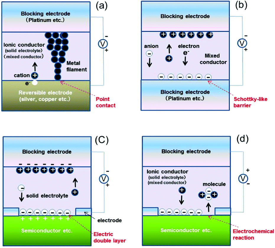 | ||
| Fig. 1 Four methods for attaining multi-functionality by controlling local ion transfers and electrochemical reactions in a nanostructure: utilization of (a) a point contact, (b) a Schottky-like barrier, (c) a solid-state electrical double layer, and (d) an electrochemical reaction. | ||
4. On-demand device capable of switching functions
By applying the point contact or the Schottky-like barrier, we constructed an on-demand device based on a new concept, namely, switching the function in the multi-function in accordance with a user's demand.12 As a single element, this device provides multi-functionality; for example, it can function as a diode, a switch, a capacitor, or an artificial synapse. The fabricated on-demand device has a laminated construction composed of a layer of platinum (Pt), a layer of tungsten oxide (WO3), and another Pt layer (see Fig. 2). The WO3 used in the device is an oxygen-deficient form (WO3−x) (formed by removing oxygen atoms by heat treatment), and it possesses mixed conductivity; that is, oxide ions (O2−) and electrons are conducted as a result of formation of oxygen vacancies.13 When a bias voltage is applied to the Pt electrodes of the device in its original (as-fabricated) state (see center illustration in Fig. 2), O2− ions are transferred within the WO3−x in accordance with the polarity and magnitude of the applied voltage, and further an electrochemical reaction occurs. If the applied bias voltage is relatively small, the O2− ions (with a negative electric charge) move near the interface with the electrode with positive polarity (see right-side illustration in Fig. 2, in which oxygen vacancies with positive charge are moved. These behaviors are same meaning). The size of the Schottky-like barrier at the interface with the electrode varies in accordance with the transfer of the O2− ions; in other words, the electronic conductivity of the device can be controlled. On the other hand, if the applied bias voltage is relatively large, in addition to the transfer of O2− ions, a reduction reaction of the WO3−x phase occurs; that is, an electron-conductive filament (composed of Magneli-phase tungsten oxide, i.e., WO3−x−δ) is formed within the WO3−x (see left-side illustration in Fig. 2). By controlling the migration of O2− ions at the interface between the formed filament and the electrode, it is possible to vary the electronic conductivity of the device even more. In other words, precisely controlling the bias voltage applied to the electrodes, in terms of magnitude as well as frequency, makes it possible to produce multiple functions that can be switched at will. | ||
| Fig. 2 Schematic diagram of an on-demand multifunction device. | ||
Various functions of the device—obtained by precisely controlling the applied voltage—are shown schematically in Fig. 3. In the case that a small voltage is applied to the device in the original (as-fabricated) device (see center illustration in Fig. 3), only the O2− ions migrate to the electrode interface. As a result, modulation of a Schottky-like barrier or formation of an electric double layer is derived, and the device functions as a capacitor (i.e., it stores charge) or a diode (i.e., it possesses a rectification property) in accordance with these two phenomena. At that time, as shown in the right- and left-side illustrations in Fig. 3, the direction of transfer of the O2− ions switches according to the polarity of the bias voltage. As a result, the dependency of the voltage polarity (according to which the device operates as a diode, capacitor, or other function) can be reversed. Moreover, the O2− ions transferred under the bias voltage return to the WO3−x−δ phase when the bias voltage is switched off; consequently, the modulation of the Schottky-like barrier can be gradually degraded and eliminated. By applying this volatile variation in electronic conduction derived at that time, it is possible to produce a short-term-memory function, namely, the mechanism of memory in the human brain.
 | ||
| Fig. 3 Ways of switching functions and performance of the on-demand multifunction device. The electronic conductive property at the interface is expressed as the signals and its magnitude of the resistance and the diode. P and N indicate the dependence of positive and negative polarity on the external field of volatile and nonvolatile electric and neuromorphic multifunctions, respectively.12 Copyright (2013) American Chemical Society. | ||
In the case that a relatively large bias voltage is applied to the device in the original state (in the center illustration in Fig. 3), as well as the O2− ions migrating to the Pt electrode interface, an electron-conductive filament is formed within the WO3−δ phase by the occurrence of a reduction reaction. As shown in the upper and lower illustrations in Fig. 3, the growth direction of the filament is reversed according to the polarity of the bias voltage. By utilizing the formation of the electron-conductive filament and the transfer of O2− ions to the interface with the electrode, it is possible to create another function, namely, a resistance switch. And the dependence of the switching operation on the bias voltage polarity (which determines the growth direction of the filament) can be reversed. The formed electron-conductive filament is stable, so its generated electronic properties are maintained even if the bias voltage is switched off. Accordingly, the state of the switch (i.e., on or off), which is attributable to the growth or disconnection of the filament, is non-volatile. Moreover, by utilizing this non-volatile variation of electrical conductivity, it is possible to reproduce the mechanism manifested as the memory of the human brain, namely, a long-term memory function by which data are not easily forgotten once stored.
Semiconductor devices developed up until now are arranged in an integrated circuit on one occasion, so it is impossible to switch the functions of the devices themselves. Moreover, to create an integrated circuit with multiple functions, it is necessary to switch the wiring that connects the devices mounted on it. Our new concept—namely, an on-demand device—provides multiple functions on single elements that can be switched at will. As a result, it is expected that the number and size of integrated circuits can be reduced while the performance of programmable circuits (which changes in accordance with the performance of integrated circuits) can be improved.
5. Superconducting device with controllable transition temperature
In recent years, it has become possible to induce conduction carriers at high density by utilizing the EDL formed by migration of ions in an electrolytic solution.14,15 The EDL can be utilized to accumulate extremely high-density carriers. It has been found that by applying the EDL, it is possible to control physical properties (such as electronic conductivity and superconductivity) in a manner hitherto impossible. However, after this approach is applied in a commercialized device, using a liquid electrolyte caused problems such as compatibility with conventional semiconductor processes and liquid leakage. By utilizing an all-solid-state EDL formed by ion transfer in a solid-state electrolyte, we have shown that it is still possible to control the above-mentioned physical properties.16 Moreover, the carrier density attained by using the all-solid-state EDL was found to be a high value in the same range as that of the liquid type (i.e., 1014 to 1015 cm−2).The set-up of experiment in which the superconducting transition temperature was varied by doping carriers (that are electrons accumulated in the niobium (Nb) surface using an all-solid-state EDL) is shown in Fig. 4(a). This device is composed of a laminated structure containing a solid electrolyte layer (lithium silicate, Li4SiO4) that conducts positively charged lithium ions (Li+ ions) to a Nb layer which is known to exhibit superconductivity. The LiCoO2/Pt layer functions not only as an electrode but also as a server that receives Li+ ions from the Li4SiO4 and supplies them to the Li4SiO4 layer. When a positive-polarity voltage is applied to the LiCoO2/Pt layer, the Li+ ions in the Li4SiO4 layer move in the direction of the Nb layer, and an EDL is formed at the interface between the Nb and Li4SiO4. The amount of charge in the EDL depends on the concentration of Li+ ions that move to the interface; consequently; the carrier concentration of electrons, in the Nb layer, accumulated by the EDL can be controlled by adjusting the applied voltage. The relationship between applied voltage and superconducting transition temperature (Tc) is plotted in Fig. 4(b). Tc of a single Nb layer (fabricated for comparison) is about 7.8 K when no voltage is applied. In contrast, it is clear from the plot that the Nb layer laminated with the Li4SiO4 layer changes Tc when a voltage is applied and that Tc can be varied in the range of 8.23 to 8.27 K by varying the applied voltage in the range of −3 to 3 V.
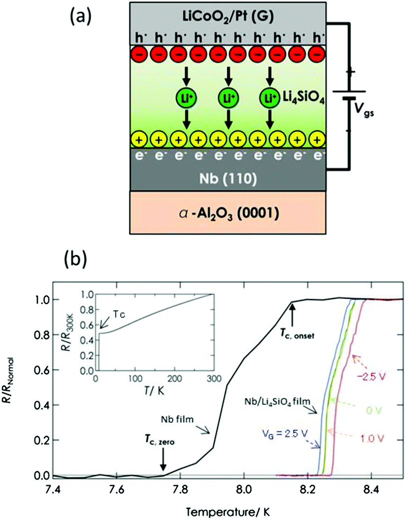 | ||
| Fig. 4 (a) A superconducting device with controllable transition temperature by injecting carriers from an all-solid-state electrical double layer. (b) Superconductivity of a Nb layer only, and changing superconductivity transition temperature of Nb in Nb/Li4SiO4 layers by migration of lithium ions to the Li4SiO4/Nb interface under an applied voltage. Superconductivity of the Nb layer only over a wide temperature range is shown in the inset.16 Copyright (2015) AIP Publishing LLC. | ||
A transistor operating as a switch (by injecting carriers into a substrate using the all-solid-state EDL) was also fabricated.17,18 This device is constructed by laminating a solid-state electrolyte (gadolinium-doped cerium oxide or yttria-stabilized zirconia (YSZ))—which conducts O2− ions or protons (H+ ions)—on a strontium titanate (SrTiO3) substrate. And it functions as a switch by means of a change in resistance due to injection of carriers from the EDL, which is formed by migration of the O2− ions or H+ ions. It is estimated that the switch can be operated at high speed (i.e., a switching time of about 1 × 10⁻¹⁰ s) by optimizing the conductivity of the protons in YSZ and the device structure.
6. Graphene oxide based transistor with controllable bandgap
A transistor that is operated by applying the electrochemical reaction between ions in an ionic conductor and a substrate (or material on the substrate) at its heterointerface has been fabricated. As one example of such a device, namely, a transistor based on graphene oxide combined with oxygen atoms in a graphene structure, is described in the following.19 Graphene oxide is a semiconductor with a bandgap whose size can be varied significantly by controlling the oxygen content. As shown in Fig. 5, regarding fabrication of the device, after graphene oxide is deposited on the substrate, a YSZ solid-state electrolyte (which predominantly conducts H+ ions at around room temperature20) is laminated on top of that. Then, to allow electrical conductivity to be measured, three-terminal platinum electrodes are formed. When a positive voltage is applied to the gate electrode (i.e., a voltage is applied across the gate electrode and the source electrode), protons carrying a positive charge in the YSZ migrate to the graphene oxide, and an electrochemical reaction between the oxygen atoms contained in the graphene oxide and the protons (i.e., 2H+ + O(graphene oxide) + 2e− → H2O) occurs. As a result of this electrochemical reaction, the oxygen atoms combined in the graphene oxide are desorbed.21 Conversely, in the case that negative voltage is applied to the gate, water (H2O) remaining in YSZ is decomposed by an electrochemical reaction (i.e., 2H+ + O(graphene oxide) + 2e− ← H2O) and the generated oxygen atoms are recombined with the graphene oxide. In other words, by effecting this electrochemical reaction by reversing the polarity of the applied voltage in a reversible manner, it is possible to vary the oxygen content of graphene oxide. And reducing the content of oxygen combined with graphene oxide makes it possible to vary the bandgap. | ||
| Fig. 5 A graphene-oxide based transistor with controllable bandgap, and the crystalline structure of graphene oxide. | ||
The experimental results shown in Fig. 6(a) demonstrate how the bandgap of graphene oxide can be controlled (in the range of 0.30 to 0.75 eV) by controlling the magnitude and polarity of the voltage applied across the gate and source electrodes. A switching characteristic is acquired in conjunction with the variability of the bandgap, and the results confirm that it can provide satisfactory operation in terms of a transistor. Furthermore, a change in the wavelength of photoluminescence (due to the variation of the bandgap) was observed. As shown in Fig. 6(b), it is possible to reversibly change the photoluminescence wavelength in the range of 400 to 700 nm by applying a gate voltage in the range of −3.5 to 2.5 V.22 Accordingly, it is being proposed that this phenomenon can be practically applied to create optical functional devices and optical sensors.
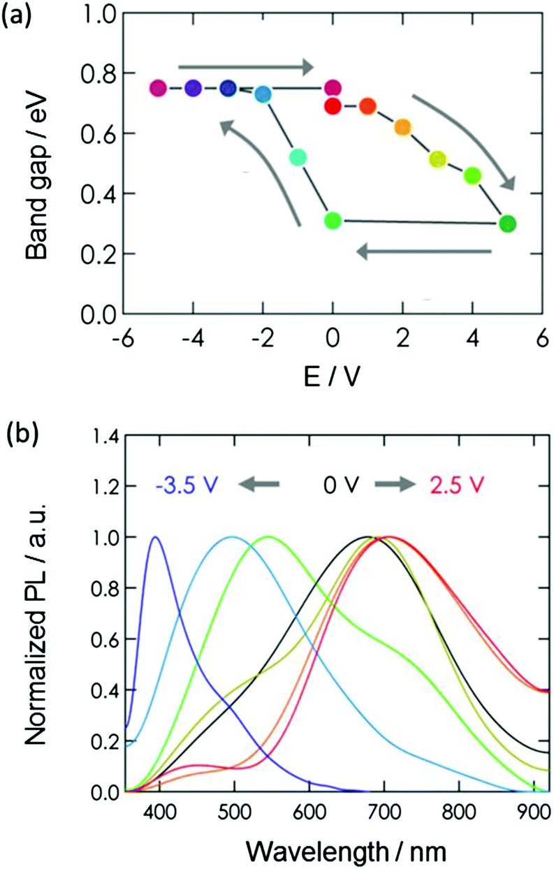 | ||
| Fig. 6 (a) Relationship between gate voltage and bandgap of graphene oxide.19 Copyright (2013) John Wiley and Sons, (b) relationship between gate voltage and photoluminescence wavelength of graphene oxide.22 Copyright (2015) American Chemical Society. | ||
7. Magnetic device with controllable magnetization and magnetoresistance
Aiming at creating spintronic devices, which operate on the basis of a new principle, we are utilizing the electrochemical reactions at the heterointerface with an ionic conductor and have formed all solid-state magnetic devices that can control magnetic properties like magnetization and magnetoresistance.23 The controls of the magnetic properties have also been achieved by utilizing migration of ions in an electrolytic solution.24,25 As shown in Fig. 7, the all solid-state device for controlling magnetization and magnetoresistance is composed of a laminated structure containing an iron oxide (Fe3O) layer, a Li4SiO4 layer and a LiCoO2/Pt layer. The LiCoO2 layer, which is a mixed Li+ ion and electron conducting oxide, is a Li+ ion supply source for the Li4SiO4 layer. Fe3O4 is an electron-conductive crystal possessing ferrimagnetism, Li4SiO4 is a solid electrolyte that can conduct Li+ ions, and LiCoO2 is a mixed conductor (i.e., it conducts both Li+ ions and electrons). As for operation of this device, when a positive voltage is applied to the LiCoO2/Pt electrode, the Li+ ions in Li4SiO4 move towards the Fe3O4 layer and are injected into Fe3O4 in accordance with an electrochemical reaction. The experimental results presented in Fig. 8(a) show that the magnetization is gradually reduced as the applied voltage is increased. The decrease in magnetization is attributable to the fact that electron carriers are also injected into Fe3O4 along with the insertion of Li+ ions, and electron carrier density and electronic structure are changed as a result. The degree of variation of magnetization depends on the amount of Li+ ions injected, which varies with the magnitude of the applied voltage. Moreover, it is possible to reversibly inject and withdraw Li+ ions to and from Fe3O4 by switching the polarity of the applied voltage; accordingly, it is also possible to reversibly control the magnetization. | ||
| Fig. 7 A magnetic device whose magnetization and magnetoresistance can be controlled by injecting and withdrawing Li+ ions to and from Fe3O4.23 Copyright (2016) American Chemical Society. | ||
 | ||
| Fig. 8 (a) Change in magnetization, (b) change in magnetoresistance effect, (c) change in electronic structure due to a reduction reaction (Fe3+ + e− → Fe2+) of iron ions accompanying injection of Li+ ions into Fe3O4, and the process of injection of Li+ ions into B sites of Fe3O4.23 Copyright (2016) American Chemical Society. | ||
The results of measuring the change in magnetoresistance that accompanies controlling the applied voltage are shown in Fig. 8(b). Under any of the applied voltages, a negative magnetoresistance (namely, resistance decreases under an externally applied magnetic field) is shown, and the decrease in resistance depends on the magnitude of the applied voltage. These results demonstrate that the magnetoresistance can also be controlled by controlling the applied voltage.
The mechanism by which the tuning of magnetization and magnetoresistance is changed by injection of Li+ ions into Fe3O4 can be explained by the change in the electronic structure presented in Fig. 8(c). In the electronic structure of Fe3O4 shown in the illustration, an electron can possess either an upward spin or a downward spin. In particular, it is known that major electrons possess downward spins near the Fermi level. Magnetization depends on the substantial spin number (namely, the proportion of all electrons with downward spin and upward spin), and the spin polarization depends on the proportions near the Fermi level. Moreover, in the Fe3O4 crystal, two kinds of Fe3+ ions (either at “A” sites or “B” sites in the illustration) exist. When Li+ ions are injected, Fe3+ ions at the B sites are reduced to Fe2+ ions, and the number of electrons with a downward spin increase. Consequently, the substantial spin number of Fe3O4 and magnetization decrease in accordance with the change in the electronic structure (shown from the left to right illustrations in Fig. 8(c)), but the spin polarization—and the magnetoresistance depending on it—increases. In other words, the observed tuning in magnetization and magnetoresistance is considered to occur because the increase and decrease in the number of electrons with a downward spin (resulting from the reduction of Fe3+ ions at the B sites to Fe2+ ions) occur reversibly.
8. Conclusions
Up until now, as next-generation information and communication devices, nanoelectronics devices have been considered a development target. However, in regard to nanoionic devices (which utilize ion transfer), interesting properties and functions that have hitherto been unattainable with conventional semiconductors have been discovered, so they are becoming popular as leading candidates for next-generation information and communication devices.As a property of nanoionic devices, ions migrate on the nanoscale or even atomic scale, and this ionic migration enables restructuring of, for example, crystal structures or interfacial structures. This restructuring is called as “nanoarchitectonics” of materials,26 and various unique physical properties and functionalities can be acquired by applying nanoarchitectonics. In other words, it can be said that a nanoionic device with nanoarchitectonics ability possesses a kind of “plasticity”; namely, it can be changed functionally and structurally on demand. This plasticity is a very important characteristic of the self-learning and neural functions, so nanoionic devices are also drawing attention in regard to application to artificial intelligence. Nanoionic devices with new functions (such as on-demand devices and artificial synapses) are already being proposed. Furthermore, it is also promising that new approaches aimed at creating brain-form computers and artificial intelligence—such as artificial nerve networks utilizing a huge amount of atomic switches (composed of self-assembled nanowires) and decision-making devices using the atomic switch that can swiftly and correctly judge options at the highest reward probability—are being taken, from now onwards. These new research studies using atomic switches are described in detail elsewhere.27–29
What's more, the expansion of condensed-matter physics might lead to the discovery of new high-temperature superconductors (created by injection of carriers and ions at high density based on nanoionic techniques), which have been difficult to create with conventional methods, or interesting magnetic properties and optical properties.
References
- T. Takahashi and O. Yamamoto, J. Appl. Electrochem., 1973, 3, 129 CrossRef CAS.
- M. Itano, Sanyo DenkiI Giho, 1972, 4, 11 Search PubMed (in Japanese).
- K. Terabe, T. Hasegawa, C. Liang and M. Aono, Sci. Technol. Adv. Mater., 2007, 8, 536 CrossRef CAS.
- C. Liang, K. Terabe, T. Hasegawa, R. Negishi, T. Tamura and M. Aono, Small, 2005, 1, 971 CrossRef CAS PubMed.
- H. Zhang, T. Tsuchiya, C. Liang and K. Terabe, Nano Lett., 2015, 15, 5161 CrossRef CAS PubMed.
- T. Sakamoto, K. Lister, N. Banno, T. Hasegawa, K. Terabe and M. Aono, Appl. Phys. Lett., 2007, 91, 092110 CrossRef.
- K. Terabe, T. Hasegawa, T. Nakayama and M. Aono, RIKEN Rev., 2001, 37, 7 CAS.
- K. Terabe, T. Haegawa, T. Nakayama and M. Aono, Nature, 2005, 47, 433 Search PubMed.
- T. Hasegawa, K. Tearbe, T. Sakamoto and M. Aono, MRS Bull., 2009, 34, 929 CrossRef CAS.
- T. Hasegawa, K. Terabe, T. Tsuruoka and M. Aono, Adv. Mater., 2012, 24, 252 CrossRef CAS PubMed.
- K. Terabe, T. Tsuruoka, A. Nayak, T. Ohno, T. Nakayama and M. Aono, Resistive Switching: From Fundamentals of Nanoionic Redox Processes to Memristive Device Applications, Wiley-VCH, 2016, p. 515 Search PubMed.
- R. Yang, K. Terabe, G. Liu, T. Tsuruoka, T. Hasegawa, J. K. Gimzewski and M. Aono, ACS Nano, 2012, 6, 9515 CrossRef CAS PubMed.
- R. Yang, K. Terabe, G. Liu, T. Tsuruoka, T. Hasegawa and M. Aono, Appl. Phys. Lett., 2012, 100, 231603 CrossRef.
- A. Tardella and J. Chazalviel, Phys. Rev. B: Condens. Matter, 1985, 32, 2439 CrossRef CAS.
- H. Shimotani, H. Asanuma, A. Tsukazaki, A. Ohtomo, M. Kawasaki and Y. Iwasa, Appl. Phys. Lett., 2007, 91, 082106 CrossRef.
- T. Tsuchiya, S. Moriyama, K. Terabe and M. Aono, Appl. Phys. Lett., 2015, 107, 013104 CrossRef.
- T. Tsuchiya, K. Terabe and M. Aono, Appl. Phys. Lett., 2013, 103, 073110 CrossRef.
- T. Tsuchiya, M. Ochi, T. Higuchi, K. Terabe and M. Aono, ACS Appl. Mater. Interfaces, 2015, 7, 12254 CAS.
- T. Tsuchiya, K. Terabe and M. Aono, Adv. Mater., 2014, 26, 1087 CrossRef CAS PubMed.
- S. Miyoshi, Y. Akao, N. Kuwata, J. Kawamura, Y. Oyama, T. Yagi and S. Yamaguchi, Chem. Mater., 2014, 26, 5194 CrossRef CAS.
- T. Tsuchiya, K. Terabe and M. Aono, Appl. Phys. Lett., 2014, 105, 183101 CrossRef.
- T. Tsuchiya, T. Tsuruoka, K. Terabe and M. Aono, ACS Nano, 2015, 9, 2102 CrossRef CAS PubMed.
- T. Tsuchiya, K. Terabe, M. Ochi, T. Higuchi, M. Osada, Y. Yamashita, S. Ueda and M. Aono, ACS Nano, 2016, 10, 1655 CrossRef CAS PubMed.
- V. Sivakumar, S. Kumar, C. Ross and Y. Shao-Horn, ECS Trans., 2007, 2, 1 Search PubMed.
- T. Yamada, K. Morita, K. Kume, H. Yoshikawa and K. Awaga, J. Mater. Chem. C, 2014, 2, 5183 RSC.
- M. Aono, Y. Bando and K. Ariga, Adv. Mater., 2012, 24, 150 CrossRef CAS PubMed.
- A. Z. Stieg, A. V. Avizienis, H. O. Sillin, R. Aguilera, H. Shieh, C. Martin-Olmos, E. J. Sandouk, M. Aono and J. K. Gimzewski, Memrister Networks, Springer, Cham, 2014, p. 173 Search PubMed.
- E. C. Demis, R. Aguilera, H. O. Sillin, K. Scharnhorst, E. J. Sandouk, M. Aono, A. Z. Stieg and J. K. Gimzewski, Nanotechnology, 2015, 26, 204003 CrossRef CAS PubMed.
- S. Kim, T. Tsuruoka, T. Hasegawa, M. Aono, K. Terabe and M. Aono, AIMS Mater. Sci., 2016, 3, 245 CrossRef.
Footnote |
| † Present address: School of Materials Science and Engineering Huazhong University of Science and Technology Wuhan 430074, P.R. China. |
| This journal is © The Royal Society of Chemistry 2016 |