 Open Access Article
Creative Commons Attribution 3.0 Unported Licence
Thermal characterization of carbon nanotube foam using MEMS microhotplates and thermographic analysis†
Cinzia
Silvestri
a,
Michele
Riccio
b,
René H.
Poelma
a,
Bruno
Morana
a,
Sten
Vollebregt
a,
Fabio
Santagata
a,
Andrea
Irace
b,
Guo Qi
Zhang
a and
Pasqualina M.
Sarro
*a
aDepartment of Microelectronics, Delft University of Technology, Feldmannweg 17, 2628CT Delft, The Netherlands. E-mail: P.M.Sarro@tudelft.nl
bDepartment of Electrical Engineering and Information Technologies, University of Naples Federico II, Via Claudio 21, 80125 Naples, Italy
First published on 31st March 2016
Abstract
Thermal material properties play a fundamental role in the thermal management of microelectronic systems. The porous nature of carbon nanotube (CNT) arrays results in a very high surface area to volume ratio, which makes the material attractive for surface driven heat transfer mechanisms. Here, we report on the heat transfer performance of lithographically defined micropins made of carbon nanotube (CNT) nanofoam, directly grown on microhotplates (MHPs). The MHP is used as an in situ characterization platform with controllable hot-spot and integrated temperature sensor. Under natural convection, and equivalent power supplied, we measured a significant reduction in hot-spot temperature when augmenting the MHP surface with CNT micropins. In particular, a strong enhancement of convective and radiative heat transfer towards the surrounding environment is recorded, due to the high aspect ratio and the foam-like morphology of the patterned CNTs. By combining electrical characterizations with high-resolution thermographic microscopy analysis, we quantified the heat losses induced by the integrated CNT nanofoams and we found a unique temperature dependency of the equivalent convective heat transfer coefficient, Hc. The obtained results with the proposed non-destructive characterization method demonstrate that significant improvements can be achieved in microelectronic thermal management and hierarchical structured porous material characterization.
1. Introduction
The performance of microelectronic and optoelectronic devices is often severely limited by high temperatures and insufficient heat management.1,2 Therefore, when considering device fabrication and packaging, it is important to select materials based on their thermal performance. The increasing demand for more integrated functionality and miniaturization of microelectronic systems, is pushing the limits of traditional cooling and packaging approaches.3 In fact, thermal management may well be the major bottleneck of the next electronics revolution. Efficient thermal management solutions are required at chip level as well as system level. For example, heat dissipation is fundamental in microprocessor and integrated circuits (ICs) as in current mobile electronic as well as server farms. Moreover, self-heating in applications like high power light-emitting diodes and solar cells affects their long-term stability.4,5 Therefore, novel cooling solutions are being developed based on nanotechnologies and functional nanomaterials.6–12 In particular, nanomaterials are mainly used as localized on-chip cooling solutions, spanning from harvesting thermal energy by using piezoelectric nanowires and super-lattice thin films,6 to heat spreading through graphene layers or nanocrystalline diamond,9–11 towards carbon nanotubes (CNTs) as thermal interface material (TIM) and heat sinks.7,8,12It is well known that carbon allotropes and their derivatives possess superior thermal properties.13 In particular, CNTs have an exceptionally high axial thermal conductivity, resulting from the strong sp2 bonds arising between the constituent carbon (C) atoms.14 In this respect, CNT-based nanofoam materials appear to be a promising candidate for achieving effective local heat dissipation.13 However, the outstanding thermal properties only apply to individual CNTs. When grown in a nanoporous network of vertically aligned CNT arrays, a remarkable drop in thermal conductivity of several orders of magnitude is observed, ranging from 0.1 to 220 W m−1 K−1.15 The main explanation for the significant thermal conductivity reduction, as compared to single CNTs, is the relative high porosity of the foam-like CNT arrays and the weak thermal coupling between neighboring nanotubes in van der Waals contact.16
However, foam-like vertically aligned CNT arrays exhibit significant advantages. Firstly, they are one of the few nanoscale materials that can be grown from a bottom-up template, which is lithographically defined and patterned using a CMOS compatible process. This makes the material extremely suitable for large-scale integration with microelectronics, replacing the need for heterogeneous integration and assembly of bulky macro-cooling solutions, such as heat sinks and fans. Secondly, the material can grow fast (growth rate of around 20 μm min−1) and can span size scales ranging from nanometers to centimeters. Therefore, it is very suitable for creating high-aspect-ratio three-dimensional (3D) microarchitectures.17 No other nanoscale material has shown similar capabilities. By combining both lithographically defined patterns and the fast vertical growth, almost infinite combinations of customized shapes and arrangements can be achieved, making the CNT nanofoam suitable for fabrication of localized, passive, customized on-chip cooling solutions, like microfins and pins, arrays and other 3D structures (Fig. S1†). Recently, we showed that high-aspect ratio foam-like CNT micropins of predefined shapes, can be grown on top of free standing membranes.18 This has highlighted the possibility to take advantage of the increased surface area, due to the high nanoporosity and high-aspect ratio of the CNT arrays, to enhance convective and radiative heat dissipation from device towards the surrounding environment. Thirdly, by combining the nanoporous morphology of vertically aligned CNTs with different nanoscale conformal coatings, we have the unique opportunity to control the functionality and tune the material properties.19 In fact, it has been demonstrated that by using thin coatings of only a few nanometers we can give a high elastic recovery to the CNT nanofoam while maintaining a high compliancy.20 This makes the nanofoam promising for thermal interface material, replacing the contaminating and difficult to apply pastes. Moreover, they have great potential to be used as low weight framework for a broad range of applications, from three-dimensional carbon electrodes,21 to thermoacoustic transducers,22 to thermochromic displays,23 to nanotexturing for solar devices.24
For analysing and predicting microelectronic system performance, it is imperative that material properties are characterized and optimized. Even though considerable research efforts have been devoted to characterize the thermal conductivity of carbon based nanomaterials, significantly less attention has been paid to the more complex interaction between gas and nanoporous material which are expressed in terms of a convective heat transfer coefficient. This coefficient is important as it accounts for a significant amount of dissipated heat, and should be included for accurate characterization of thermal performance. The heat transfer coefficient across the solid–gas interface and its variation with the pressure, has been measured for a single nanowire in a gas environment by Cheng et al.25 However, no experimental data can be found in literature discussing the natural convective heat transfer coefficient of foam-like vertically aligned CNT arrays and its temperature dependency at micron scale. Moreover, thermal investigations on CNT arrays are often carried out at relatively low temperature, thus the thermal radiative heat transfer is often negligible.26 Foam-like CNT arrays have a large surface area to volume ratio. When combined with the almost perfect black body radiative properties, significant radiative losses at low temperature can be achieved.27
In this work, we report on the heat dissipative properties of lithographically defined foam-like CNT arrays in vacuum and in the natural convective regime. To perform these thermal measurements a novel experimental approach was developed combining MEMS microhotplates (MHPs), on which the nanofoam materials are grown, with high-resolution thermographic analysis. Using direct growth of CNTs on the chip we can limit contact resistance, handling of the samples and benefit more directly from the intrinsic properties of the nanofoam material. Using a MHP device as both the heating source and as integrated thermal sensor, we characterize under a steady-state temperature condition several CNT arrays patterned in different configurations. We quantify the equivalent natural convective heat transfer coefficient between solid–air interface (Hc), the radiative heat transfer coefficient (Hrad) and the CNT nanofoam effective thermal conductivity (keff) over a wide temperature range. The present work demonstrates the effectiveness of lithographically defined CNT nanofoam structures as on-chip cooling solutions for consumer electronics.
2. Experimental
Performing thermal measurements on nano- and microscale CNT structures is challenging. Difficulties arise from handling the material, controlling contributions from contact resistances, towards a simple lack of an appropriate measurement apparatus with sufficient resolution. In this paper, we develop a measurement approach that combines a microelectromechanical systems-based (MEMS) experimental platform with high-resolution IR thermographic imaging, providing several advantages. First of all, the material to be analyzed is directly grown on our measurement device; hence no complex sample handling or further processing is needed. Moreover, there is no additional contact resistance due to assembly of the material on the measurement apparatus. Lastly, the MEMS integrated temperature sensor and power controller have a high accuracy because they are placed within nanometer distance from the material to be analyzed.2.1 CNT growth on microhotplates
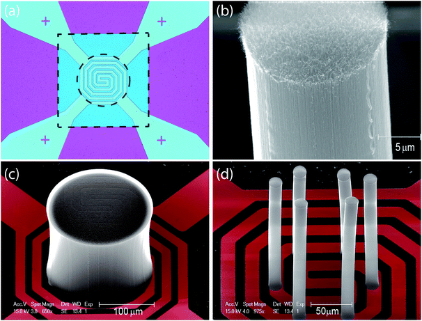
High-aspect ratio foam-like CNT micropins in lithographically defined locations are directly grown on top of a suspended MEMS microhotplate (Fig. 1). The MHP consists of a low-stress 400 nm thick SiNx square membrane with an area of 1 mm2, in which a platinum (Pt) microheater is integrated, as shown in ESI (Fig. S2†). The microheater has a spiral geometry, which covers a central area of 330 μm × 330 μm with a thickness of 200 nm (Fig. 1(a)). A detailed description of the MHP fabrication process can be found in previous work.18 After the MHP fabrication, the micropins are grown using low-pressure chemical vapor deposition (CVD) in a commercial deposition system (Aixtron, Black Magic) at 600 °C for 5 minutes, on lithographically defined catalyst (Fe) areas. An Aluminum Oxide (Al2O3) layer of 10 nm thick and 1.5 nm of Fe are used as barrier and catalyst layer, respectively (Fig. S3†). The as-synthesized CNT micropin consists of interlaced multiwalled carbon nanotubes (MWCNTs) held together by weak van der Waals interactions. As determined by scanning electron microscopy (SEM, Philips XL50) inspection, the MWCNTs have an average diameter of 9 nm, and are packed with a density of 112 tubes μm−2 resulting in a porosity of about 95%. These values are in agreement with those reported by others.20,28 The packing density of our foam-like CNT micropin is limited by the relatively large spacing between the iron (Fe) nanoparticles employed as catalyst for the CVD growth. In Fig. 1(b) a close up view of the foam-like morphology of the tip of a CNT micropin is shown. We prepared two different sample configurations: the first configuration consists of a single CNT micropin of 200 ± 1 μm in diameter and 158 ± 2 μm in height (Fig. 1(c)). The second configuration consists of multi-pins where each of the six micropins has a diameter of 20 ± 1 μm and a height of 180 ± 4 μm (Fig. 1(d)).2.2 Electrical characterization
The employed MHP design generates a local hotspot in the center of the suspended membrane. The heat produced by Joule heating is dissipated by conduction through the membrane towards the bulk substrate, and by radiation and convection towards the surrounding medium. The addition of the CNTs enhances the heat dissipation through convection and radiation. To quantify the heat dissipated by the as-grown CNT micropins, electrical measurements were performed in air and in vacuum. The difference in power dissipated towards the environment is measured by operating the MHP at equivalent temperatures for the different sample configurations and environmental conditions. The dissipated power was acquired in steady-state heat transfer conditions at various temperatures, ranging from ambient temperature (Tsurr = 294.15 K) up to a maximum temperature Tmax of 575 K. For reference, the measurements were repeated on a MHP without CNTs. The electrical characterization is performed in a customized stainless steel chamber equipped with four probe needles connected to an Agilent 4156C Parameter Analyzer (Fig. S4†). After connecting the chamber with a vacuum pump, the device was characterized from atmospheric pressure up to 1 × 10⁻⁵ mbar, which is the minimum pressure achievable in the system. All the configurations are measured by supplying a step wise current from 1 mA to 10 mA. The maximum input current is limited by the breakdown current of the heater, which occurs at around 14 mA. The MHP is used both as local heat source and as sensing element. For the latter functionality, it is necessary to first calibrate the Pt spiral heater. The temperature coefficient of resistance (TCR) obtained is equal to 2500 ± 40 ppm K−1. After recording the voltage drop across the microhotplate, the resulting resistance is related to the temperature using the measured TCR value.2.3 Infrared (IR) micro-thermography
High-resolution thermographic microscopy analysis can be used as an effective method to extract thermal conductivity of vertically oriented CNT composites.29 In our case the experimental IR thermal analysis was performed with a state-of-art system based on the use of an ultrafast thermo-camera.30 Before performing IR measurements on CNT configurations, a calibration procedure was performed to compensate for different material IR emissivity, temperature ranges and lens addition. The calibration procedure, based on the two point algorithm, is described elsewhere.31 After the calibration step, the temperature distribution on the device top surface was recorded at four different power dissipation levels by heating the device by Joule heating. The high-resolution micro-thermography system has a temperature sensitivity of about 1 K and a spatial resolution of 2.5 μm. Fig. S5† reports the high reliability between the average temperature measured by both IR thermal analysis and electrical stimulation for the micropin and multi-pin configurations.2.4 Theoretical analysis
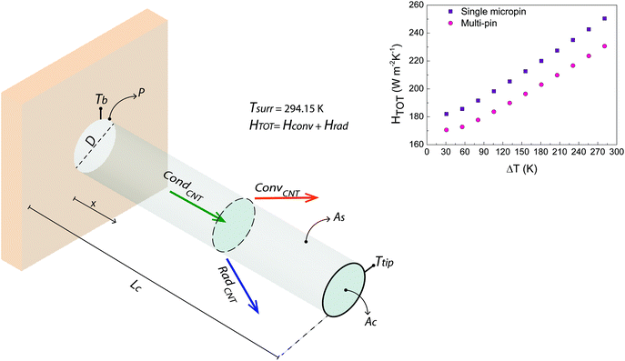
To evaluate the heat transport in a foam-like CNT micropin, the governing differential equation for a pin fin system subjected to appropriate boundary conditions is used.32Fig. 2 shows a schematic illustration of a single CNT micropin with length L = 180 μm and diameter D = 20 μm. As the micropin height L is much larger than the phonon mean free path, a diffusive heat transport regime can be applied. The estimated phonon mean free path in a MWCNT array can be as low as 20 nm due to defect scattering and intertube coupling.33Moreover, the conduction along the CNT micropin is assumed to be one-dimensional because of the high aspect ratio (L ≫ D), hence the radial temperature variation is negligible compared to the axial variation. The one-dimensional heat transfer model described above is used to extract the micropin effective conductivity keff, from the measurements. The detailed description about the analytical model can be found in ESI.†
3. Results and discussion
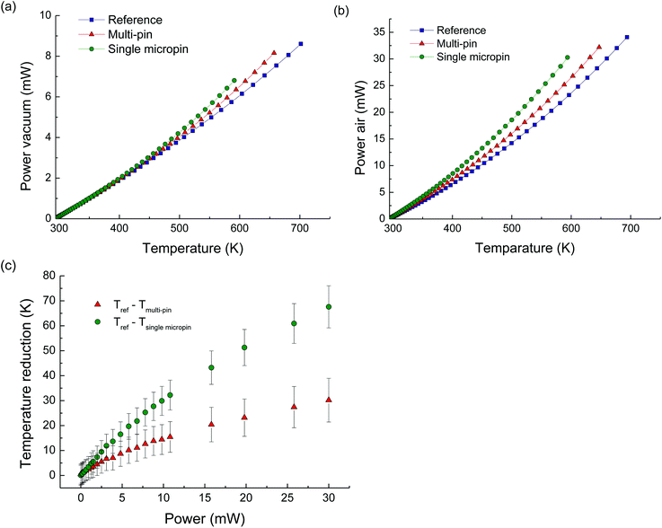
The measurement of MHP electric driving power and the temperature for all sample configurations in both vacuum and air is shown in Fig. 3.In vacuum, all sample configurations show a similar relationship between power and temperature up to 450 K. At higher temperatures, the microhotplates equipped with CNT micropins start diverging, by dissipating more power for an equivalent temperature, as compared to the reference sample without CNT structures (Fig. 3(a)). This is due to the additional heat loss through radiation. The radiation heat loss is directly proportional to the total exposed surface area At and to the material emissivity ε, consequently the increase of both results in more power dissipated. The single- and multi-micropin CNT configuration increase the MHP surface area with respectively 0.163 mm2 and 0.073 mm2. Combined with the high emissivity coefficient of carbon, it explains why the single micropin configuration dissipates more power compared to the multi-pin one in vacuum.
In air, the power versus temperature measurements start diverging at a lower temperature, namely 350 K, see Fig. 3(b). The natural convection, in addition to radiative heat transfer, is now contributing to a better thermal performance for all three sample configurations. However, the addition of the CNT micropins enhances the radiative and convective heat transfer even further, as shown by the offset in Fig. 3(b) with respect to the reference (no CNT) sample, thus reducing the temperature at the center of the MHP. For a given input power of 30 mW, the single micropin and multi-pin arrangements show a remarkable reduction in the local hot spot temperature of respectively 66 ± 8 K and 28 ± 8 K (Fig. 3(c)). In Section 3.1 we discuss in more detail the effects of nanoporosity on the enhanced convective heat transfer.
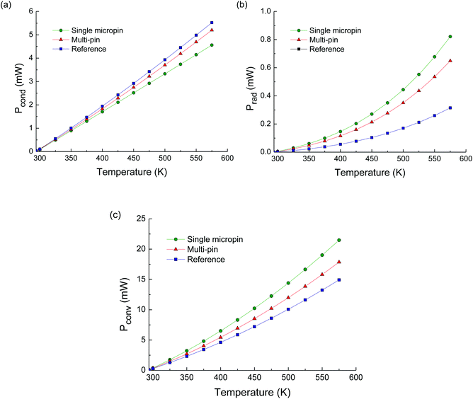
In order to estimate the contribution of each heat transfer mechanism involved, we first calculate the radiative dissipation, Prad, by the Stefan–Boltzmann law: Prad(Tavg) = εσAt(Tavg4 − Tsurr4), where σ is the Stefan–Boltzmann constant (5.67 × 10⁻⁸ W m−2 K−4), ε is the effective emissivity of the surface, Tavg and Tsurr are the average temperature measured from the MHP and the surrounding temperature, respectively. The heat transferred by conduction, Pcond, is obtained from the MHP driving power in vacuum Pvac, minus the power dissipated by radiation: Pcond(Tavg) = Pvac(Tavg) − Prad(Tavg). The convective heat transfer Pconv, is obtained by subtracting the MHP driving power in air Pair, and the input power in vacuum: Pconv(Tavg) = Pair(Tavg) − Pvac(Tavg). Fig. S6† shows the cooling paths across the entire system (MHP and CNT micropin). In Fig. 4 the power versus temperature measurements of conduction, convection and radiation are reported for all sample configurations. It is interesting to observe that for a given temperature, the power dissipated by conduction through the membrane is lower for the reference MHP than for the MHP with integrated CNT micropins (Fig. 4(a)). This is because more power is dissipated by radiation and convection through the CNT micropins, as shown in Fig. 4(b and c). We also notice that the power dissipated by radiation increases upon the integration of the micropins. At Tmax = 575 K, the increase in radiative dissipated power for the multi- and single micropin corresponds to about 106% and 161%, respectively, compared to the reference hotplate. The power dissipated by convection increases less significantly, 20% and 44%, respectively. In all cases the power is mainly dissipated by convection. This is shown in Table S1,† where the relative power dissipated through conduction, radiation and convection are reported at Tmax = 575 K.
In the following subsections we further explore the CNT nanofoam thermal properties in terms of the natural convective heat transfer coefficient Hc, radiative heat transfer coefficient Hrad and effective thermal conductivity keff.
3.1 Natural convective heat transfer coefficient
Convective heat dissipation is an important factor that influences the overall thermal behavior of the MHP and nanofoam material. The temperature dependence of the natural convective heat transfer coefficient Hc is defined by:34 | (1) |
Fig. 5(a) shows the dependency of Hc on temperature. For the single micropin configuration Hc increases from 179 W m−2 K−1 to 241 W m−2 K−1, when ΔT is increased from 30 K to 280 K. In the same temperature range, the Hc for the multi-pin configuration increases from 167 W m−2 K−1 to 222 W m−2 K−1. The achieved values for the heat transfer coefficients are much higher than those recorded at the macroscale, which typically range between 2 and 25 W m−2 K−1 in gases. Therefore, at micrometer scale, the natural convection is subjected to a considerable enhancement. The increased value of Hc is an indicator of the influence of surface effects such as increased surface area, due to nanoporosity, surface friction, surface roughness, surface geometry on the flow and heat transfer at micro- and nanometer scale.35 A similar enhancement has been recorded for cylinders and plates with characteristic length around 100 μm.36
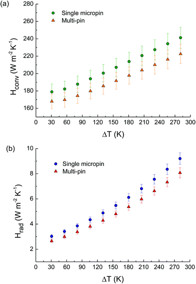 | ||
| Fig. 5 (a) Convective heat transfer coefficient (Hc) and (b) radiative heat transfer coefficient (Hrad) extracted from the electrical measurement performed on the device equipped with the single micropin and the multi-pin. The uncertainty in the experimental data was calculated applying the method developed by Kline and McClintock.39 | ||
The power-temperature characteristics of the microhotplate are not significantly influenced by the orientation in the gravitational field. The change in operational power to maintain the MHP at a constant temperature, with regards to vertical or horizontal orientation, was less than 1%. This suggests that the heat-to-air transfer mechanism is dominated by the conduction between the heated solid interface and the air molecules, whereas the natural convective motion is negligible. It has been experimentally demonstrated that the heat loss by natural convection from electrically heated microfilaments is mainly transferred through air conduction rather than through air convection.37,38 In particular, it has been reported that the conductive contribution to Hc is almost ten times higher than the convective contribution. Therefore, Hc at micro and nanoscale has to be considered as an equivalent convective heat transfer coefficient. It includes both the natural convection and conduction to surrounding air, with the latter as dominant heat dissipation mechanism. Our results as well as the literature demonstrate that a more complex interaction between heat exchange of microstructures, nanofoam materials and the surrounding fluid is present.
3.2 Radiative heat transfer coefficient
The radiative heat transfer coefficient Hrad and its temperature dependency are determined by,| Hrad = εσ(Tavg2 + Tsurr2)(Tavg + Tsurr). | (2) |
To precisely quantify the radiative contribution, the ε of the MHP and the CNTs is measured by high-resolution IR thermal microscopy. The ε of the CNT nanofoam is 0.95, which is very close to that of a black body; while the ε of the MHP is only about 0.22. Fig. 5(b) shows the obtained Hrad trends for both CNT micropin arrangements. For the single micropin configuration Hrad increases from 2.7 W m−2 K−1 to 9.2 W m−2 K−1 when ΔT is increased from 30 K to 280 K. For the multi-pin, Hrad goes from 2.4 W m−2 K−1 to 8.0 W m−2 K−1 for the same temperature range. As expected, the radiative emission increases with both temperature and emitting area.
3.3 Thermal conductivity
The effective thermal conductivity keff of a micropin extracted from the multi-pin arrangement can be determined by using the one-dimensional heat transfer model coupled with high-resolution IR thermal maps (Fig. 6). Equation S6,† can be solved for keff by extracting the base temperature, Tb, and tip temperature, Ttip, of each micropin from the obtained thermal mapping. The measured thermal conductivity keff is averaged over the six CNT micropins. By powering the MHP while recording the emitted infrared radiation, it is possible to determine the spatial temperature distribution and consequently the corresponding temperature dependency of keff over a broad temperature range, from room temperature up to 510 K.Fig. 7(a) shows the obtained keff as a function of temperature. The CNT nanofoam keff increases gradually when the temperature increases, reaching about 2.18 ± 0.04 W m−1 K−1 at 510 K. The effective thermal conductivity increased by 39.1% over a temperature range of 369 K to 406 K. Above 406 K the nanofoam showed reduced rates equal to 25.6% and down 19.5% at 406–450 K and at 450–508 K, respectively. The conductivity slope variation is caused by the competition between the various phonon-scattering processes triggered by temperature change. In CNT nanofoam, we observed a continuous increase of the thermal conductivity, also above the typical peak temperature of individual CNTs.40 It likely reveals a dominance of point-defect and grain-boundary scatterings over Umklapp scattering even at high temperature.
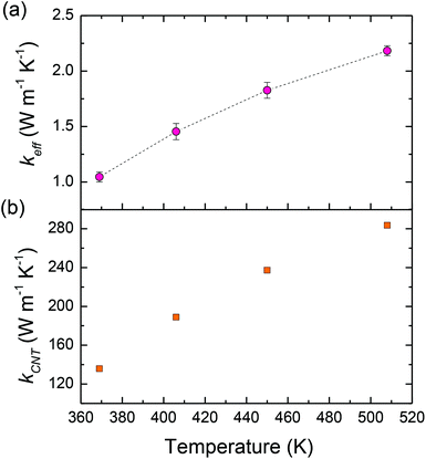 | ||
| Fig. 7 (a) Temperature dependence of the effective thermal conductivity of a foam-like CNT micropin. (b) Temperature dependence of the estimated individual CNT thermal conductivity. | ||
The temperature dependence of the vertically aligned MWCNT array thermal conductivity has been reported at different temperature ranges: at 5–390 K,41 at 10–300 K,42 and at 300–830 K.43 In order to investigate keff as a function of temperature, the cited work employed complex post-growth process and experimental techniques, which can affect the CNT quality and adds a potential source of error and uncertainty during the measurement phase. For example, suspending a CNT rope between two copper electrodes is a manually intensive procedure,42,43 and when successful, infiltration of the contact material into the CNT arrays can influence the achieved result.41 Our non-destructive thermal transport measurement, allows the direct characterization of nano- and micro-scale materials at a large temperature range. Furthermore, no sample handling is required when the materials can be grown from the bottom-up in predefined locations on the microhotplate.
The thermal conductivity of an individual MWCNT in vertically aligned arrays, kCNT, can be estimated by correlating keff with the number of CNTs per unit area (NCNT/Aarray) and the average cross sectional area of a single nanotube (ACNT):44
 | (3) |
Fig. 7(b) reports the obtained kCNT considering a nanotube average diameter of 9 nm. At the lowest investigated temperature kCNT is about 136 W m−1 K−1. The estimated value is affected by uncertainties in defining the CNT packing density within the CNT nanofoam.
| keff ∼ 0.007 kCNT. |
Both kCNT and keff are orders of magnitude lower than the experimental value of individual MWCNT (∼3000 W m−1 K−1). The quality of the CNTs, which typically depends on the growth method, is the main factor influencing the intrinsic thermal conductivity. The Raman spectra of the CNT samples show an ID/IG ratio equal to 0.93, revealing a low crystallinity degree within the CNT nanofoam (Fig. S7†). It is well known that, in comparison to laser ablation or arch-discharge methods, CNTs grown by chemical vapor deposition (CVD) have considerably lower quality. However, the thermal conductivity drop observed goes beyond factors related to the CNT quality like packing density, number of shells and dislocations.
The major factors degrading the overall CNT nanofoam thermal performance are the interface thermal resistance between adjacent tubes and the thermal boundary at the interface CNT–substrate. The interaction between adjacent nanotubes, primarily caused by van der Waals forces, creates new sites for phonon scattering, decreasing the intrinsic thermal conductivity, and enhancing the interface thermal resistance between neighboring CNTs. Aliev et al. found that the inter-tube interactions and alignment imperfections reduce the thermal conductivity of a MWCNT arrays to a factor of three.27 In particular, they estimated that to decrease the inter-tube scattering, the crosslinking between nanotubes should occur only over short distances (2–3% of their total length). In our work, considering a micropin length of about 180 μm, the maximum overlapping length between neighboring tubes should be between 3.6 μm and 5.4 μm. This would prevent the degradation of the heat conduction. Careful inspection of the nanofoam morphology using SEM, indicates that crosslinking of nanotubes is higher than the suggested optimum value (Fig. S8†). This suggested that the inter-tubes interactions might significantly contribute to the observed thermal conductivity reduction.
The thermal boundary resistance at the interface CNT–substrate is considered an important limiting factor for both potential thermal and electrical applications. It depends strongly on the substrate material and packing density.44 It has been demonstrated that in presence of a weak bond between substrate and the nanofoam, not all the CNTs participate effectively to the heat transport.45
4. Conclusions
Lithographically defined CNT nanofoam structures, can enhance the surface driven heat transfer mechanisms of microelectronic systems in the natural convective regime. Different configurations of CNT structures were directly grown on MEMS microhotplates (MHPs) with controllable hotspot and integrated temperature sensor. Combined with high-resolution infrared thermographic microscopy analysis, the thermal material properties of the patterned CNT structures were measured. Our approach eliminated measurement uncertainties arising from manual assembly and handling of samples. Augmentation of the MHP hotspot with CNT micropins (with a height of 158 ± 2 μm and a diameter of 20 ± 1 μm) resulted in a temperature reduction of up to 66 ± 8 K in free air, compared to MHPs without micropins operating at similar power. In particular, the equivalent convective heat transfer coefficient Hc for a multi-pin configuration accounted for 167 W m−2 K−1, much higher than macroscale value (between 2 to 25 W m−2 K−1). We conclude that the conduction between the air molecules and the heated solid interface dominates the heat-to-air transfer mechanism, whereas the natural convective motion is marginal. The CNT nanofoam also demonstrated a gradually increase of the effective thermal conductivity with temperature from: 1.04 W m−1 K−1 at 369 K to 2.24 W m−1 K−1 at 510 K. Finally, the lithographically defined CNT nanofoam structures are suitable for large-scale integration with microelectronics and represent a valuable alternative to bulky macro-cooling solutions. We therefore believe that CNT nanofoam structures are suitable for localized, passive, customized on-chip cooling solutions, like micro-fins, pin arrays and other 3D microarchitectures.Acknowledgements
This work was supported by NanoNextNL, a micro and nanotechnology consortium of the Government of the Netherlands and 130 partners. The authors gratefully acknowledge the technical staff of the Else Kooi Laboratory (former DIMES Technology Center) at TU Delft for the support in device fabrication.Notes and references
- S. Kaur, N. Raravikar, B. a. Helms, R. Prasher and D. F. Ogletree, Nat. Commun., 2014, 5, 141–144 CrossRef PubMed.
- D. D. Lu and C. P. Wong, Materials for advanced packaging, Springer US, 2009 Search PubMed.
- J. Cho and K. E. Goodson, Nat. Mater., 2015, 14, 136–137 CrossRef CAS PubMed.
- S. Buso, G. Spiazzi, M. Meneghini and G. Meneghesso, IEEE Trans. Device Mater. Reliab., 2008, 8, 312–322 CrossRef.
- I. T. Sachs-Quintana, T. Heumüller, W. R. Mateker, D. E. Orozco, R. Cheacharoen, S. Sweetnam, C. J. Brabec and M. D. McGehee, Adv. Funct. Mater., 2014, 24, 3978–3985 CrossRef CAS.
- I. Chowdhury, R. Prasher, K. Lofgreen, G. Chrysler, S. Narasimhan, R. Mahajan, D. Koester, R. Alley and R. Venkatasubramanian, Nat. Nanotechnol., 2009, 4, 235–238 CrossRef CAS PubMed.
- Q. Liang, X. Yao, W. Wang, Y. Liu and C. P. Wong, ACS Nano, 2011, 5, 2392–2401 CrossRef CAS PubMed.
- C.-T. Hsieh, C.-E. Lee, Y.-F. Chen, J.-K. Chang and H.-S. Teng, Nanoscale, 2015, 7, 18663–18670 RSC.
- Z. Yan, G. Liu, J. M. Khan and A. a. Balandin, Nat. Commun., 2012, 3, 827 CrossRef PubMed.
- J. Zhang, G. Shi, C. Jiang, S. Ju and D. Jiang, Small, 2015, 11, 6197–6204 CrossRef CAS PubMed.
- V. Goyal, A. V. Sumant, D. Teweldebrhan and A. A. Balandin, Adv. Funct. Mater., 2012, 22, 1525–1530 CrossRef CAS.
- K. Kordás, G. Tóth, P. Moilanen, M. Kumpumäki, J. Vähäkangas, A. Uusimäki, R. Vajtai and P. M. Ajayan, Appl. Phys. Lett., 2007, 90, 123105 CrossRef.
- A. a. Balandin, Nat. Mater., 2011, 10, 569–581 CrossRef CAS PubMed.
- S. Berber, Y. Kwon and D. Tomanek, Phys. Rev. Lett., 2000, 84, 4613–4616 CrossRef CAS PubMed.
- A. Volkov and L. Zhigilei, Appl. Phys. Lett., 2012, 101, 043113 CrossRef.
- R. S. Prasher, X. J. Hu, Y. Chalopin, N. Mingo, K. Lofgreen, S. Volz, F. Cleri and P. Keblinski, Phys. Rev. Lett., 2009, 102, 1–4 CrossRef PubMed.
- M. De Volder, S. Park, S. Tawfick and A. J. Hart, Nat. Commun., 2014, 5, 4512 CAS.
- C. Silvestri, B. Morana, G. Fiorentino, S. Vollebregt, G. Pandraud, F. Santagata, G. Q. Zhang and P. M. Sarro, in 2014 IEEE 27th International Conference on Micro Electro Mechanical Systems (MEMS), IEEE, 2014, pp. 48–51.
- R. H. Poelma, B. Morana, S. Vollebregt, E. Schlangen, H. W. van Zeijl, X. Fan and G. Q. Zhang, Adv. Funct. Mater., 2014, 24, 5737–5744 CrossRef CAS.
- R. H. Poelma, X. Fan, Z.-Y. Hu, G. Van Tendeloo, H. W. van Zeijl and G. Q. Zhang, Adv. Funct. Mater., 2016, 26, 1233–1242 CrossRef CAS.
- P. E. T. Al, S. Park, P. Dong-Won, C.-S. Yang, K.-R. Kim, J.-H. Kwak, H.-M. So, C. W. Ahn, B. S. Kim, H. Chang and J.-O. Lee, ACS Nano, 2011, 5, 7061–7068 CrossRef PubMed.
- Y. Wei, X. Lin, K. Jiang, P. Liu, Q. Li and S. Fan, Nano Lett., 2013, 13, 4795–4801 CrossRef CAS PubMed.
- P. Liu, L. Liu, K. Jiang and S. Fan, Small, 2011, 7, 732–736 CrossRef CAS PubMed.
- C. L. Pint, K. Takei, R. Kapadia, M. Zheng, A. C. Ford, J. Zhang, A. Jamshidi, R. Bardhan, J. J. Urban, M. Wu, J. W. Ager, M. M. Oye and A. Javey, Adv. Energy Mater., 2011, 1, 1040–1045 CrossRef CAS.
- C. Cheng, W. Fan, J. Cao, S. G. Ryu, J. Ji, C. P. Grigoropoulos and J. Wu, ACS Nano, 2011, 5, 10102–10107 CrossRef CAS PubMed.
- J. Hone, M. C. Llaguno, N. M. Nemes, a. T. Johnson, J. E. Fischer, D. a. Walters, M. J. Casavant, J. Schmidt and R. E. Smalley, Appl. Phys. Lett., 2000, 77, 666 CrossRef CAS.
- A. E. Aliev, M. H. Lima, E. M. Silverman and R. H. Baughman, Nanotechnology, 2010, 21, 035709 CrossRef PubMed.
- S. Vollebregt, R. Ishihara, F. D. Tichelaar, Y. Hou and C. I. M. Beenakker, Carbon, 2012, 50, 3542–3554 CrossRef CAS.
- A. M. Marconnet, N. Yamamoto, M. a. Panzer, B. L. Wardle and K. E. Goodson, ACS Nano, 2011, 5, 4818–4825 CrossRef CAS PubMed.
- G. Romano, M. Riccio, G. De Falco, L. Maresca, A. Irace and G. Breglio, in 2014 Semiconductor Thermal Measurement and Management Symposium (SEMI-THERM), IEEE, 2014, pp. 80–84.
- M. Riccio, A. Pantellini, A. Irace, G. Breglio, A. Nanni and C. Lanzieri, Microelectron. Reliab., 2011, 51, 1725–1729 CrossRef CAS.
- F. P. Incropera, D. P. DeWitt, T. L. Bergman and A. Lavine, Fundamentals of Heat and Mass Transfer, John Wiley & Sons, 7th edn, 2007 Search PubMed.
- D. Yang, Q. Zhang, G. Chen, S. Yoon, J. Ahn, S. Wang, Q. Zhou, Q. Wang and J. Li, Phys. Rev. B: Condens. Matter, 2002, 66, 2–7 Search PubMed.
- A. Pike and J. W. Gardner, Sens. Actuators, B, 1997, 45, 19–26 CrossRef CAS.
- Z. Y. Guo and Z. X. Li, Int. J. Heat Mass Transfer, 2003, 46, 149–159 CrossRef.
- J. Peirs, D. Reynaerts and H. Van Brussel, Proceedings. 1998 IEEE Int. Conf. Robot. Autom. (Cat. No.98CH36146), 1998, 2, pp. 1516–1521.
- I. Langmuir, Phys. Rev., 1912, 34, 401–422 CAS.
- I. Brody and F. Korösy, J. Appl. Phys., 1939, 10, 584–596 CrossRef.
- S. J. Kline and F. A. McClintock, Mech. Eng., 1953, 75, 3–8 Search PubMed.
- P. Kim, L. Shi, A. Majumdar and P. L. McEuen, Phys. Rev. Lett., 2001, 87, 215502 CrossRef CAS PubMed.
- M. B. Jakubinek, M. A. White, G. Li, C. Jayasinghe, W. Cho, M. J. Schulz and V. Shanov, Carbon, 2010, 48, 3947–3952 CrossRef CAS.
- W. Yi, L. Lu, Z. Dian-lin, Z. Pan and S. Xie, Phys. Rev. B: Condens. Matter, 1999, 59, R9015–R9018 CrossRef CAS.
- X. Huang, J. Wang, G. Eres and X. Wang, Carbon, 2011, 49, 1680–1691 CrossRef CAS.
- A. M. Marconnet, M. a. Panzer and K. E. Goodson, Rev. Mod. Phys., 2013, 85, 1295–1326 CrossRef CAS.
- M. a. Panzer, G. Zhang, D. Mann, X. Hu, E. Pop, H. Dai and K. E. Goodson, J. Heat Transfer, 2008, 130, 052401 CrossRef.
Footnote |
| † Electronic supplementary information (ESI) available: SEM image of customized shapes of high-aspect ratio CNT nanofoams, 3D sketch and cross-section of MHP, CNT growth process on MHP. Measurement setup, comparison between temperature recorded by electrical characterization and IR mapping. Thermal paths across the device, relative power dissipated by all configurations at 575 K in air. Detailed one-dimensional heat transfer model. Raman spectra, schematic and SEM image of overlapping CNTs. See DOI: 10.1039/c6nr00745g |
| This journal is © The Royal Society of Chemistry 2016 |

