
 Open Access Article
 This Open Access Article is licensed under a
 Creative Commons Attribution 3.0 Unported Licence
Carbon![[thin space (1/6-em)]](https://www.rsc.org/images/entities/h2_char_2009.gif) :nickel nanocomposite templates – predefined stable catalysts for diameter-controlled growth of single-walled carbon nanotubes†
:nickel nanocomposite templates – predefined stable catalysts for diameter-controlled growth of single-walled carbon nanotubes†
Svetlana
Melkhanova
ab,
Miro
Haluska
c,
René
Hübner
a,
Tim
Kunze‡
b,
Adrian
Keller§
a,
Gintautas
Abrasonis
a,
Sibylle
Gemming
abd and
Matthias
Krause
*a
aHelmholtz-Zentrum Dresden-Rossendorf, Bautzner Landstraße 400, 01328 Dresden, Germany. E-mail: matthias.krause@hzdr.de
bTechnische Universität Dresden, cfaed, 01062 Dresden, Germany
cMicro and Nanosystems, DMAVT ETH Zürich, 8092 Zürich, Switzerland
dTechnische Universität Chemnitz, 09107 Chemnitz, Germany
First published on 19th July 2016
Abstract
Carbon![[thin space (1/6-em)]](https://www.rsc.org/images/entities/char_2009.gif) :nickel (C:Ni) nanocomposite templates (NCTs) were used as catalyst precursors for diameter-controlled growth of single-walled carbon nanotubes (SWCNTs) by chemical vapor deposition (CVD). Two NCT types of 2 nm thickness were prepared by ion beam co-sputtering without (type I) or with assisting Ar+ ion irradiation (type II). NCT type I comprised Ni-rich nanoparticles (NPs) with defined diameter in an amorphous carbon matrix, while NCT type II was a homogenous C:Ni film. Based on the Raman spectra of more than 600 individual SWCNTs, the diameter distribution obtained from both types of NCT was determined. SWCNTs with a selective, monomodal diameter distribution are obtained from NCT type I. About 50% of the SWCNTs have a diameter of (1.36 ± 0.10) nm. In contrast to NCT type I, SWCNTs with a non-selective, relatively homogeneous diameter distribution from 0.80 to 1.40 nm covering 88% of all SWCNTs are obtained from NCT type II. From both catalyst templates predominantly separated as-grown SWCNTs are obtained. They are free of solvents or surfactants, exhibit a low degree of bundling and contain negligible amounts of MWCNTs. The study demonstrates the advantage of predefined catalysts for diameter-controlled SWCNT synthesis in comparison to in situ formed catalysts.
:nickel (C:Ni) nanocomposite templates (NCTs) were used as catalyst precursors for diameter-controlled growth of single-walled carbon nanotubes (SWCNTs) by chemical vapor deposition (CVD). Two NCT types of 2 nm thickness were prepared by ion beam co-sputtering without (type I) or with assisting Ar+ ion irradiation (type II). NCT type I comprised Ni-rich nanoparticles (NPs) with defined diameter in an amorphous carbon matrix, while NCT type II was a homogenous C:Ni film. Based on the Raman spectra of more than 600 individual SWCNTs, the diameter distribution obtained from both types of NCT was determined. SWCNTs with a selective, monomodal diameter distribution are obtained from NCT type I. About 50% of the SWCNTs have a diameter of (1.36 ± 0.10) nm. In contrast to NCT type I, SWCNTs with a non-selective, relatively homogeneous diameter distribution from 0.80 to 1.40 nm covering 88% of all SWCNTs are obtained from NCT type II. From both catalyst templates predominantly separated as-grown SWCNTs are obtained. They are free of solvents or surfactants, exhibit a low degree of bundling and contain negligible amounts of MWCNTs. The study demonstrates the advantage of predefined catalysts for diameter-controlled SWCNT synthesis in comparison to in situ formed catalysts.
Introduction
Carbon nanotubes have been known for more than 20 years1 and since the very first reports on their synthesis fascinating electronic properties of CNTs were predicted. It was expected that they will be used in many fields of molecular electronics, viz. in transistors,2–4 medical devices,5,6 chemical and biochemical sensors7,8etc. However, in currently commercialized applications CNTs are mainly used as additives to improve the mechanical, thermal, and electrical properties of bulk materials (resins, plastics, polymers).9 Semiconducting SWCNTs are well suited for transistors because of their low electron scattering and small bandgap.10 For “high-tech” applications, however, precisely-defined electronic properties are needed. This requires eventually one specific diameter and chiral angle of SWCNTs.11,12 There are several methods of CNTs synthesis,13–15 and among them CVD is the most versatile and most easily scalable one. The structural and morphological properties of CVD-grown CNTs are affected by many process parameters,15 such as the carbon precursor nature and concentration, carrier gas pressure and composition, temperature, time, catalyst nature and size, etc. There are many reports that catalyst particles must have a suitable size in order to be active for CNT growth and that the control of the catalyst nanoparticles before and during CVD is very important in order to control CNT yield, diameter and chirality. The most used catalysts for CNT growth are Fe,16–31 Co,24,32–45 Ni17,23,46–53 and their bimetallic alloys.38,42,54–56 The CNT synthesis on these catalysts may produce SWCNTs with narrow diameter distribution and few chiralities depending on the catalyst nanoparticle size.16,20,21,25,26,32,35,41,51,54In almost all studies, the catalysts are prepared in situ by an initial annealing step of the precursor prior to CVD or by precursor injection during the CVD process. The control of catalyst size and shape depends on many process parameters in a complex manner, whose optimization often requires numerous iterations.27 The process could be simplified by introducing catalyst templates with predefined NP size and shape, which exhibit sufficient stability against coalescence and grain coarsening. Carbon:nickel nanocomposite (C:Ni NC) thin films of 10 nm to 100 nm thickness have been grown in a large variety of microstructures. This was achieved by variation of deposition temperature (RT to 500 °C) and Ni concentration (5 to 30 at% Ni) during thin film growth without and with irradiation by an assisting low-energy Ar+ beam. So far, C:Ni NCs were reported with NP diameters from 1.5 nm to 17 nm, spherical and columnar shapes, and in regular or stochastic three-dimensional particle arrangements.57–59 In our previous work on SWCNT growth48 we reported the successful growth of individual SWCNTs with a Gaussian-like, non-selective diameter distribution of (1.6 ± 0.4) nm from 10 nm thick templates consisting of columnar Ni NPs of (4.0 ± 1.0) nm diameter before the CVD growth process.
In this work, the SWCNT diameter distributions obtained by CVD from two 2 nm thick C:Ni NC template types are compared. NCT type I comprises predefined catalyst NPs, while for NCT type II the catalyst NPs are formed in situ during the CVD process. This approach enables a direct comparison of the SWCNT growth from pre-defined and in situ formed catalyst particles. Transmission electron microscopy (TEM) and scanning electron microscopy (SEM) were applied to characterize the NCTs before and after the CVD process and to determine the size distribution of the catalyst particles. SWCNT diameter distribution and the presence of multi-walled CNTs were analysed by SEM and Raman spectroscopy. It is demonstrated that SWCNT diameters strongly depend on the NCT type applied for CVD synthesis. Using NCT type I about 50% of the SWCNTs have a diameter of (1.36 ± 0.10) nm, while SWCNTs with a relatively homogeneous diameter distribution from 0.8 nm to 1.4 nm are obtained from NCT type II. Furthermore it is shown that MWCNT formation, SWCNT bundling, and catalyst NP coarsening are successfully suppressed. Finally, the possibilities and limits of SWCNT diameter control by defining the catalyst NP size are discussed.
Experimental
The NCT type I (C:Ni, ∼15 at% Ni) was deposited at 300 °C by ion beam co-sputtering of a graphite/Ni zone target onto a Si/SiO2 (∼0.5 μm, thermally oxidized) substrate. Template type II (C:Ni, ∼8 at% Ni) was prepared at RT by irradiating the growing C:Ni film with an oblique incidence angle (∼60°) assisting Ar+ beam of 130 eV ion energy. The sputter ion source (Kaufmann type, IonTech Inc., Fort Collins, USA) was operated with an Ar+ ion energy of 1 keV and a beam current of 40 mA, the assisting ion source (Kaufmann type, ISQ40KF, Ion-Tech GmbH, Wüstenbrand, Germany) with Ar+ energies of 50 to 130 eV and a total beam current of 9 mA. The base pressure in the deposition chamber was (1.3 ± 0.3) × 10−5 Pa, the working pressure was about 10−2 Pa, and the deposition time was 3 to 4 min. The given film composition was extrapolated from the Rutherford Backscattering analysis of our previous work.57–59 Further deposition details are described ibid.
The subsequent CVD process consists of two consecutive steps: the NCT pre-treatment and the CNT growth. For this, the C:Ni templates were placed in the CVD oven (Black Magic, Aixtron) and exposed to flowing air (flow rate 200 sccm, pressure 2 to 3 mbar) for 10 min at 550 °C. After 10 min the reactor was evacuated, the temperature was increased to 735 °C, and the samples were exposed to a mixture of C2H2/H2/Ar (5/300/300 sccm; total pressure 5.1 mbar) for ∼20 min.
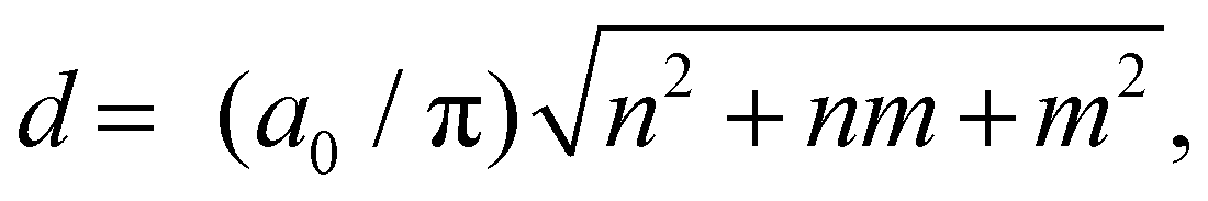
Cross-sectional transmission electron microscopy images of C:Ni thin films were obtained using an image Cs-corrected Titan 80–300 (FEI) microscope operated at an acceleration voltage of 300 kV. TEM specimens of the C:Ni templates before CNT growth were prepared by sawing, grinding, dimpling, and final Ar ion milling. TEM lamella preparation of the C:Ni templates after pre-treatment and CNT growth was done by in situ lift-out using a Zeiss Crossbeam NVision 40 system. To protect the sensitive surface, a carbon cap layer was deposited beginning with electron beam assisted and subsequently followed by Ga focused ion beam (FIB) assisted precursor decomposition. Afterwards, the TEM lamella was prepared using a 30 keV Ga FIB with adapted currents. Its transfer to a 3 post copper lift-out grid (Omniprobe) was done with a Kleindiek micromanipulator. To minimize sidewall damage, Ga ions of only 5 keV energy were used for final thinning of the TEM lamella to electron transparency. SEM of the NCTs before and after CVD growth of the CNTs was performed by detecting secondary electrons using a S-4800 microscope (Hitachi) operated at an accelerating voltage of 10 kV. Raman maps of randomly selected sample areas of 20 × 20 μm2 were recorded with a step width of 1.25 μm using a micro-Raman Labram HR spectrometer, which is equipped with a holographic 1800 lines per mm grating and a liquid nitrogen cooled CCD detector (Horiba-Jobin-Yvon). The laser wavelengths of 532 nm and 632.8 nm, corresponding to photon energies of 2.33 eV and 1.96 eV, respectively, were used for excitation. The obtained Raman spectra were fitted using an in-house software routine based on a Levenberg-Marquardt least-square algorithm. SWCNT diameter distributions were calculated by using the relation dSWCNT = 232 cm−1 nm/νRBM,60 wherein νRBM represents the Raman shift of the radial breathing mode of SWCNTs, and by sorting the obtained diameter values into diameter intervals of 0.05 nm width.
Results
The microstructure of the original NCT type I is heterogeneous and consists of Ni-rich particles embedded in an amorphous carbon (a-C) matrix (Fig. 1). Cross-sectional TEM analysis gives a mean NP diameter of (2.0 ± 0.3) nm, which corresponds to the average NCT thickness. The NPs appear to be well-aligned with a mean NP center to center distance of (4.3 ± 0.3) nm. Lattice fringes were resolved for approximately 40% of 27 NPs analyzed in detail (Fig. 1b and c). Fast Fourier Transform (FFT) analysis gave lattice spacings grouped into (a) 0.22 nm to 0.24 nm and (b) 0.20 to 0.21 nm. In one case crossed lattice fringes with spacings of 0.21 nm and 0.15 nm enclosing an angle of 46° were observed. The latter values are in good agreement with reference data of the (006) and {116} planes of rhombohedral Ni3C (rh-Ni3C), which are 0.215 nm, 0.156 nm, and 43.4°.61 Moreover, the group (a) lattice fringe spacings are indicative for rh-Ni3C, namely for its {110} planes.61 Group (b) spacings could be assigned either to rh-Ni3C or to fcc-Ni. According to these findings, previous own work, and the literature on this material system, the initial Ni-rich phase of NCT type I is assigned to rh-Ni3C.57,62–64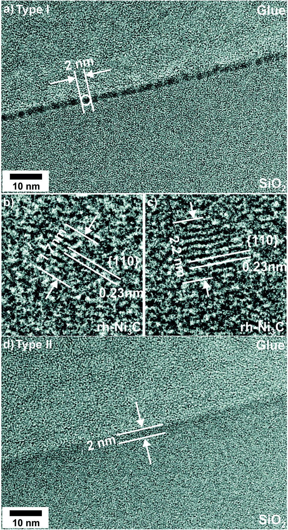 | ||
| Fig. 1 Cross-sectional TEM images of C:Ni templates before the CVD process of CNTs: (a)–(c) NCT type I; (d) NCT type II. Images (b) and (c) are enlarged views of micrograph (a) showing selected crystalline Ni3C NPs in NCT type I. | ||
The cross-sectional TEM image of NCT type II (Fig. 1d) shows the formation of a Ni-enriched layer appearing darker than the SiO2 substrate and the resin glue on top of the film, which is used for TEM specimen preparation. The layer thickness is 2 nm and hence the same as for the NCT type I. In contrast to NCT type I, no NP formation was detected for NCT type II (Fig. 1d). The homogenous microstructure of C:Ni NCT type II is attributed to the hyperthermal particle and energy flux of the irradiating Ar+ ions. It causes ion-enhanced mixing and partial re-sputtering of Ni, which lead to a homogenous distribution of the metal in the a-C matrix.
After CVD growth of CNTs the morphology of NCT I consists of individual NPs as before the CVD process (Fig. 2). Cross-sectional TEM revealed moderate NP coarsening accompanied by broadening of the diameter distribution from initially (2.0 ± 0.3) nm to (3.0 ± 0.7) nm (Fig. 3). The NPs are less aligned and the NCT surface appears rougher than before the CVD process. Lattice fringes were observed for 72% out of 29 NPs studied in detail. FFT analysis revealed the coexistence of Ni-rich NPs with hcp (Fig. 2b) and fcc (Fig. 2c) lattice structure in an approximately equal ratio. The details of this analysis are provided in the ESI.† The FFT of the nanocrystal in Fig. 2b corresponds very closely to a [1![[2 with combining macron]](https://www.rsc.org/images/entities/char_0032_0304.gif) 1
1![[3 with combining macron]](https://www.rsc.org/images/entities/char_0033_0304.gif) ] zone axis image of hcp-Ni (for details see ESI, Fig. 1†).65 It has the same Ni sublattice structure as rh-Ni3C. The nanocrystal displayed in Fig. 2c has fcc crystal structure. Its FFT corresponds to a [011] zone axis image of fcc-Ni (for details see ESI, Fig. 2†).65 One out of 29 FFT patterns showed lattice fringes with spacings of 0.22 nm and 0.25 nm enclosing an angle of 56°. One possible assignment would be fcc-NiO, although the observed spacings were enlarged by about 4% compared to the reference.61 Alternatively, this FFT pattern might be described by Ni3C {110} and {014} lattice fringes, whose spacings are 0.22 nm and 0.25 nm with an interplanar angle of 56.7°.
] zone axis image of hcp-Ni (for details see ESI, Fig. 1†).65 It has the same Ni sublattice structure as rh-Ni3C. The nanocrystal displayed in Fig. 2c has fcc crystal structure. Its FFT corresponds to a [011] zone axis image of fcc-Ni (for details see ESI, Fig. 2†).65 One out of 29 FFT patterns showed lattice fringes with spacings of 0.22 nm and 0.25 nm enclosing an angle of 56°. One possible assignment would be fcc-NiO, although the observed spacings were enlarged by about 4% compared to the reference.61 Alternatively, this FFT pattern might be described by Ni3C {110} and {014} lattice fringes, whose spacings are 0.22 nm and 0.25 nm with an interplanar angle of 56.7°.
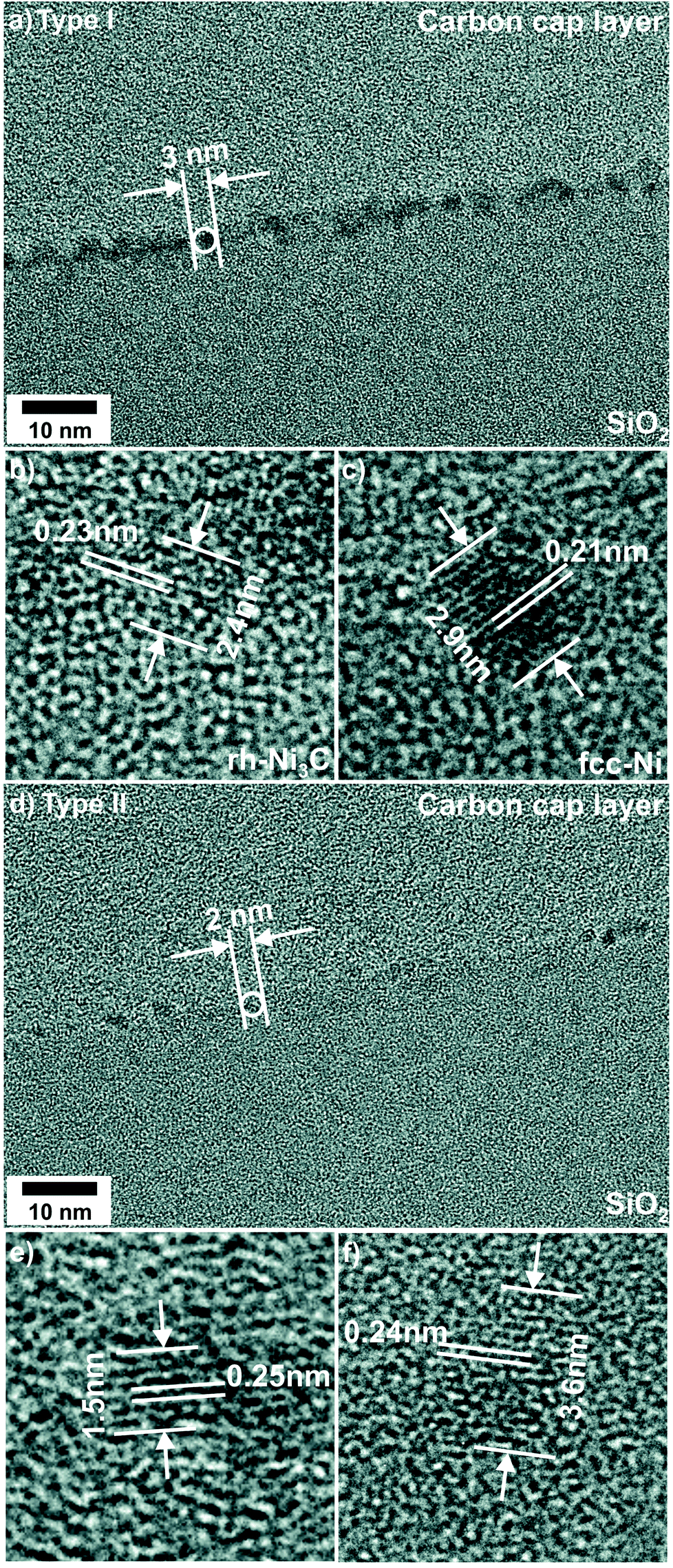 | ||
| Fig. 2 Cross-sectional TEM images of C:Ni templates after CVD growth of CNTs: (a)–(c) NCT type I; (d)–(f) NCT type II. Images (b) and (c) [(e) and (f)] show selected crystalline NPs in NCT type I [NCT type II]. | ||
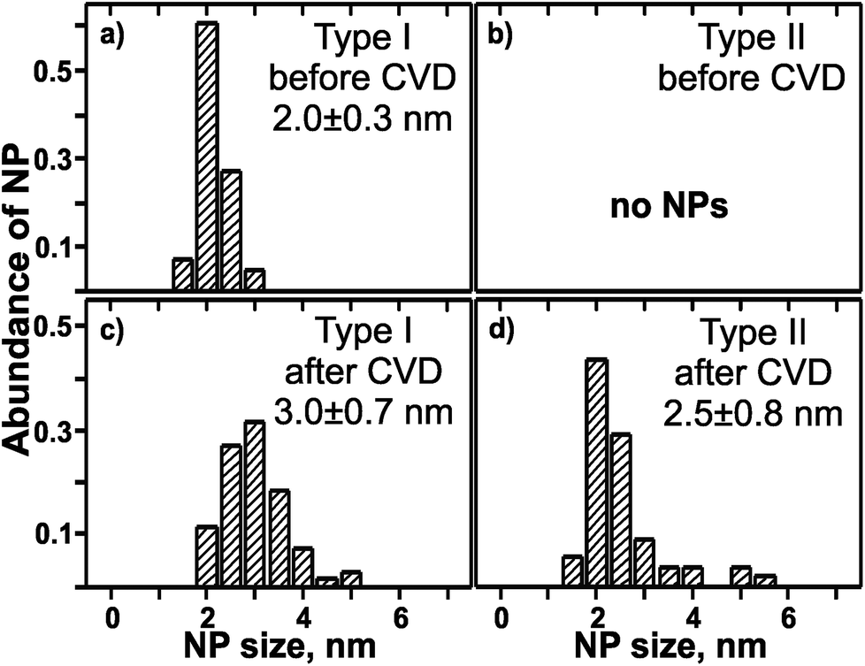 | ||
| Fig. 3 Normalized size distributions of Ni-rich NPs measured by TEM before and after the CVD process, respectively. NCT type I, (a) and (c), NCT type II, (b) and (d). | ||
In summary, approximately 50% of NCT type I NPs changed their lattice structure from rh-Ni3C to fcc-Ni. For another approximately 50% the observed hcp-Ni lattice structure points to the conservation of the initial rh-Ni3C phase structure. The formation of fcc-NiO could not be verified. Finally it should be noted that TEM analysis is not suitable to provide information about the structure of the a-C matrix.
The morphology of NCT type II, where initially only a contrast enhancement with respect to SiO2 substrate and resin glue could be detected, was completely changed during the CVD process. The initial homogenous and 2 nm thick Ni-enriched layer was no more detected. Instead, NCT type II is characterized by the coexistence of ranges without (major fraction) and with (minor fraction) separated NPs after the CVD (Fig. 2d). Their average diameter is (2.5 ± 0.8) nm (Fig. 3). The smallest resolved NP had a diameter of 1.5 nm. Two dominant lattice spacings were identified by FFT analysis, namely 0.21 nm and 0.25 nm. Their assignment to rh-Ni3C, fcc-Ni, or fcc-NiO is ambiguous as outlined in the previous sections, and supporting interplanar angles could not be determined. The NP formation from NCT type II can be considered as an example for the SWCNT growth using catalysts, which are formed in situ during the process of pre-treatment and CVD. The post-CVD NP diameter distribution of NCT type I is narrower than that of NCT type II. This difference can be expressed as relative deviation from the mean NP diameter values. It is 23% for NCT type I and 32% for NCT type II. Moreover, compared to NCT type II, a larger fraction of NCT type I NPs showed lattice fringes. This is a hint for a larger degree of NP crystallinity in NCT type I than in type II after the CVD growth of CNTs.
The TEM results show that the microstructure of the pre-defined NCT type I is largely preserved during the CNT growth process. Its mean NP diameter grew by about 1 nm (ca. 50%), and the fraction of crystalline NPs within the template increased. In contrast to that NCT type II underwent a complete re-structuring from a homogenous film into a film of NPs. The NP size distribution for NCT type II after CVD is sufficiently narrow and can be compared with the one obtained from metallic thin films. As an example, pre-annealing of a 0.22 nm-thin Ni film produced NPs with diameter of (4.4 ± 0.6) nm.52
In contrast to the featureless appearance before nanotube growth, SEM images of the NCT samples measured after the CVD process display three types of features: (i) randomly distributed spherical spots of less than 10 nm in diameter, (ii) bent objects of about 80 nm length, and (iii) blurred objects of up to 3 μm length (Fig. 4). These features are assigned to metallic nanoparticles, multi-walled CNTs (MWCNTs), and single-walled CNTs, respectively. The NP diameters are apparently larger for NCT type I than for type II. The amount of MWCNTs is generally very low. In NCT type II samples MWCNTs are virtually absent. The statistical analysis of the SEM images points to a similar efficiency of both types in catalyzing SWCNT growth with yields of ∼5 to 7 tubes per μm2.
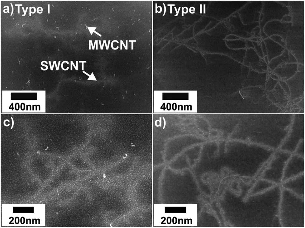 | ||
| Fig. 4 SEM images of C:Ni templates after CVD growth of CNTs: (a), (c) NCT type I; (b), (d) NCT type II. Compared to the few MWCNTs the individual SWCNTs appear blurred and diffuse due to charging effects and probably also due to thermally-induced vibrations. | ||
Raman spectroscopy enables a non-destructive and simple determination of the SWCNT diameter because of the inverse proportionality of diameter and radial breathing mode (RBM) frequency. Hence, the diameter distribution of SWCNTs in the sample can be conveniently elucidated by measuring Raman spectra with two or more excitation laser wavelengths, for example, 532 nm and 632.8 nm. This approach allows detecting SWCNTs in the diameter range from 0.6 nm to 2.3 nm. The reliability of the SWCNT diameter distribution obtained by this method was confirmed by parallel Raman and High-Resolution TEM studies in the literature.16,37
Typical Raman spectra in the range of the RBM obtained during 2D Raman mapping with two excitation wavelengths for NCT types I and II are shown in Fig. 5a and b. The vast majority of the spectra contains only one single RBM line. In total, the Raman spectra of more than 600 individual SWCNTs were analysed in this study. The RBM line widths for SWCNTs grown with both template types cover the range of 4 cm−1 to 8 cm−1. They decrease with increasing RBM frequency, similar to the results reported previously in the literature.66 The narrow line widths point to long lifetimes of the excited RBM modes, and indicate a high degree of structural order and a negligible contribution of defect-induced phonon decay processes. Such a behavior is consistent with the formation of individual SWCNTs with a low amount of structural defects.67 In order to analyze the abundance of SWCNTs, the observed RBM frequencies were assigned to frequency intervals of 10 cm−1 width and subsequently summed. The analysis shows a diameter-selective SWCNT formation for NCT type I: 50% of all observed tubes have RBM frequencies from 160 cm−1 to 180 cm−1 (Fig. 5c). In contrast to that, a broad distribution of RBM frequencies is found for NCT type II (Fig. 5d). The corresponding diameter distributions of SWCNTs (normalized to 1) are shown in Fig. 6. The SWCNT diameter distribution depends strongly on the template type. The diameter distribution of NCT type I reveals an astonishingly high selectivity for SWCNTs of the diameter interval centered at (1.360 ± 0.025) nm, which includes about 33% of the SWCNTs (Fig. 6a). Moreover, 51% of all synthesized SWCNTs fall into a narrow diameter range of 1.26 nm to 1.46 nm.
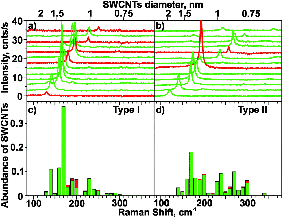 | ||
| Fig. 5 Selected RBM range Raman spectra (a, b) and RBM distributions (c, d) of SWCNTs formed from C:Ni templates: (a), (c) NCT type I; (b), (d) NCT type II. The color code represents spectra measured with 532 nm (green) and 632.8 nm (red) laser excitation, respectively. | ||
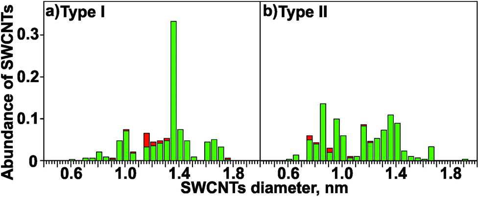 | ||
| Fig. 6 Normalized diameter distributions of SWCNTs synthesized from C:Ni templates as derived from the abundance of observed RBM lines in the corresponding diameter intervals: (a) NCT type I; (b) NCT type II. The color code represents data obtained with 532 nm (green) and 632.8 nm (red) laser excitation, respectively. | ||
Applying the formula for the nanotube diameter d,
The proposed diameter selectivity is further supported by the following findings of the Raman analysis. The next thinner SWCNTs, which are expected to be in resonance with laser radiation of 532 nm, would be (13,6), (14,4) and (15,2) with diameters of 1.32 nm, 1.28 nm and 1.26 nm and RBM frequencies of 175 to 185 cm−1, respectively. Their abundance is only of the order of 5% (Fig. 6). At slightly larger diameters than (1.360 ± 0.025) nm the SWCNTs (15,5), (11,10) and (14,7) with 1.41 nm, 1.43 nm and 1.45 nm should resonate with 532 nm laser excitation. The abundance of this fraction is about 7%. That means that the low and high limit of the SWCNT diameter distribution maximum is precisely defined for NCT type I.
It can be further concluded that semiconducting tubes with diameters of ∼1.6 nm and RBM frequencies of around 140 cm−1 contribute only to a minor extent to the observed diameter distribution (Fig. 6). Finally, for 632.8 nm laser excitation, the most abundant SWCNTs have RBM frequencies of around ∼200 cm−1 for NCT type I. They belong to metallic tubes with a diameter of 1.2 nm, whose M11 transition is in resonance with the laser energy of 1.96 eV. These metallic tubes cause the local maximum in the diameter distribution for 632.8 nm laser excitation, but their contribution to the overall SWCNT diameter distribution is of the order of less than 5%.
In contrast to type I, NCT type II yields a relatively uniform distribution of SWCNT diameters from 0.8 to 1.4 nm (88% of all SWCNTs). The gap of the diameter distribution at about 1.15 nm, which is also observed for NCT type I, is explained by the missing resonance of such SWCNTs with 532 nm laser radiation. For this reason the diameter distribution is not described as bimodal but as uniform. The upper limit of the SWCNT diameter distribution obtained with NCT type II is defined by the very low amount of SWCNTs with an RBM frequency of about 140 cm−1 (<5%) corresponding to diameters of about 1.7 nm. The high overall yield of SWCNT with small diameters (40% in the 0.6–1.0 nm range) is however remarkable.
Since NCT type I is apparently a very promising pre-defined and stable catalyst for diameter-selective SWCNT growth, its morphology after pre-treatment was investigated. For this purpose the growth process was terminated after the pre-treatment step (exposing the NCTs to flowing air at 550 °C for 10 min) and the pre-treated template was analyzed using cross-sectional TEM and Raman spectroscopy (Fig. 7). The Raman spectra of NCT type I show the typical sp2-carbon (sp2-C) Raman lines, i.e. the D line at around 1350 cm−1 and the G line at around 1550 cm−1, before and after pre-treatment (Fig. 7a). The intensity of the sp2-C Raman lines decreased to 30% after the pre-treatment, and simultaneously the intensity of the Si-2TO lines at around 950 cm−1 increased by approximately 40% (not shown). These observations point to a partial loss of a-C, presumably by oxidation to CO2. Moreover, narrower line widths and G line up-shift indicate a higher degree of graphitization of the a-C matrix. Cross-sectional TEM analysis reveals a mean NP diameter of (2.2 ± 0.4) nm, which is the same as in the virgin NCT within the experimental accuracy. In conclusion, the pre-treatment step causes slight roughening of NCT type I due to partial removal of the embedding a-C matrix. These changes have apparently no effect on the NP morphology.
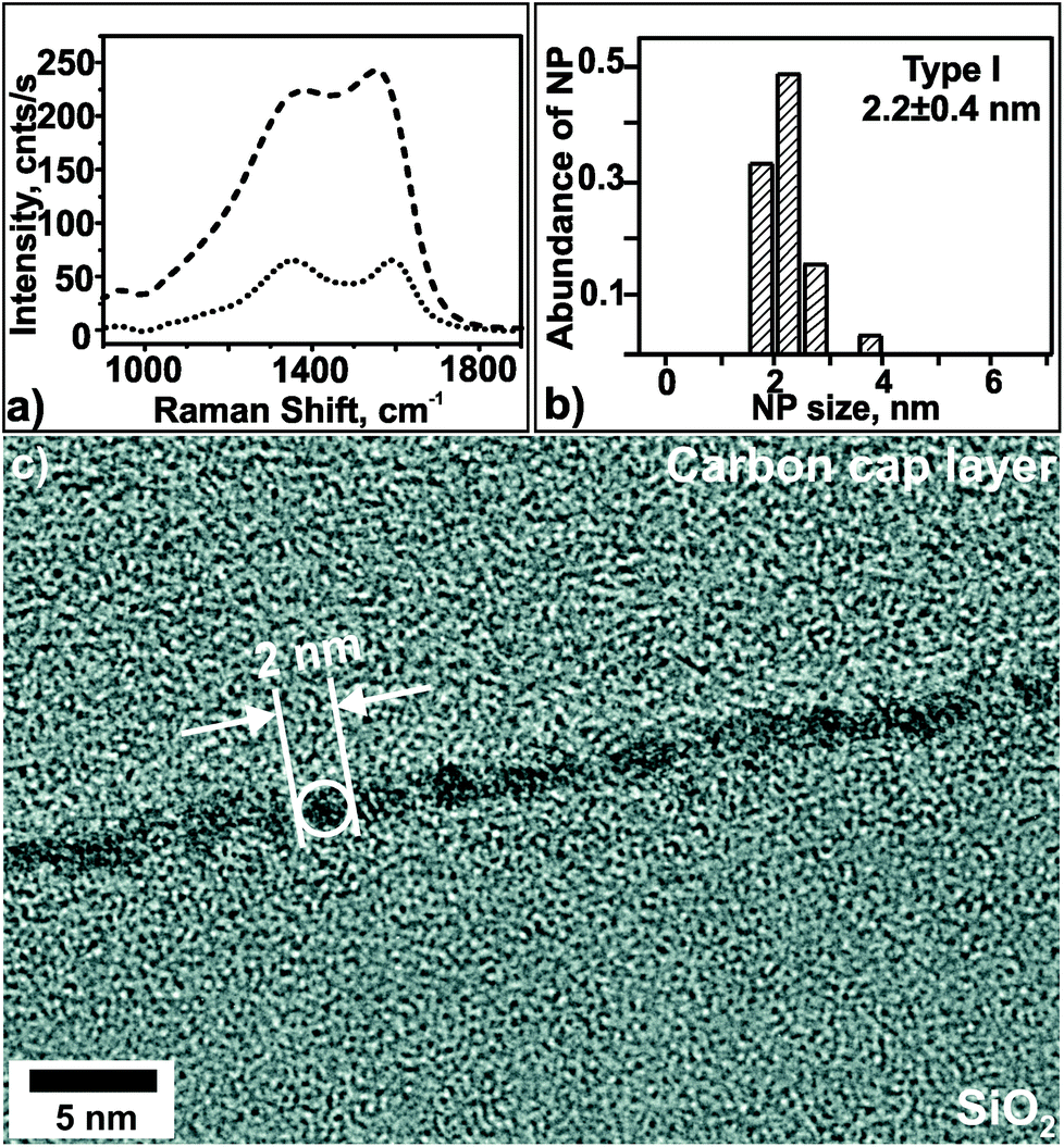 | ||
| Fig. 7 Characterization of NCT type I after the pre-treatment step: (a) Raman spectrum (dotted line) in comparison to that of the pristine template (dashed line), (b) normalized size distribution of Ni-rich NPs measured by TEM, (c) cross-sectional TEM image. | ||
Discussion
In the following section the conclusions from the presented results for CVD growth of SWCNTs using C:Ni NCTs with and without predefined NPs are discussed.
(a) NP stability of NCT type I.
Without stabilization, Ni thin films on SiO2 surfaces undergo clustering via surface diffusion for temperatures larger than −173 °C.70,71 Ni cluster diameters of 8 nm to 20 nm were reported for nominally 1 nm thick Ni films.71,72 Bulk diffusion of Ni into a SiO2 layer on Si and formation of NiSi2 starts at elevated temperatures (≥425 °C), depending on SiO2 thickness. The bulk diffusion onset temperature for a 2.5 nm thick SiO2 layer was reported to be 800 °C.70 These data demonstrate that without stabilization much larger Ni particles are formed at temperatures similar to those during catalyst pre-treatment and CVD growth in the present study.
In fact, our investigations have shown that a defined microstructure of Ni-rich NPs with narrow diameter distribution of (2.0 ± 0.3) nm can be stabilized up to temperatures of 735 °C and used to grow SWCNTs. This has been achieved by embedding the NPs in a protective matrix of a-C, forming a NCT of type I. The protective a-C is fully stable in ambient conditions and allows easy handling of the NCTs in air. Thus, the a-C matrix ensures the safe transport of the templates and their transfer into the CVD oven. During the pre-treatment step at 550 °C in air, the a-C matrix is partially conserved. This ensures that the Ni-rich NPs keep their initial positions, diameter distribution and spacing. In this way the NPs are prevented from coagulation and grain coarsening. This observation is attributed to the strong interaction between Ni and C, which is e.g. larger than that between Ni and SiO2.73 The rest of the a-C matrix presumably undergoes oxidation to CO2. After pre-treatment, the NCT type I enters the CVD synthesis with pre-defined, almost unchanged diameter in activated form.
(b) Relation between SWCNT and catalyst properties.
It is obvious to explain the narrower and apparently selective SWCNT diameter distribution obtained by CVD growth using NCT type I by the pre-defined NP diameters and their demonstrated stability. As a consequence, the carbon precursors are exposed to almost equally-sized catalytically active NPs during the CVD process. In contrast to that situation, the initially homogenously distributed Ni in NCT type II undergoes a coarsening, the carbon precursor is exposed to catalytic particles of different size and as a consequence, the SWCNT distribution is broader and not selective. On the other hand the smaller SWCNT diameters obtained with NCT type II can be attributed to the fact that NPs grow from an initially homogenous Ni distribution to a size of (2.5 ± 0.8) nm. The behavior of NCT type II resembles catalysts whose catalytically active particles are formed in situ from metal thin films during the CVD process. The results presented here demonstrate that narrower SWCNT diameter distributions are accessible by the use of pre-defined, stable catalyst templates.
Apparently the best strategy to obtain SWCNTs with narrow diameter distribution is to use a catalyst with stable NPs of predefined size and to prevent them from coarsening during the CVD process. Several approaches to realize these preconditions were described in the literature. First, the catalyst NPs can be sparsely distributed over the inert substrate so that the large distance between the particles would prevent their aggregation.21,23,44,53 For instance, Paillet et al.53 studied the CVD synthesis of SWCNTs on Ni NPs with the mean size of (4.7 ± 1.4) nm using C2H4 as a carbon source. The narrow size distribution of SWCNTs was achieved at 850 °C when the density of NPs and the synthesized SWCNTs was small (40 and 100 NPs per μm2 led to 0.1–0.2 and ∼3 SWCNTs per μm2, respectively). Importantly, for these conditions the Ni NPs had the same size before and after the CVD. An increase of the surface density to several hundred NPs per μm2 led to aggregation of NPs and formation of amorphous carbon and big filamentous structures. An increase of the reaction temperature to 950 °C also resulted in larger Ni NPs with broader size distribution.53 In our work, a narrow SWCNT diameter distribution was successfully obtained with a much higher density of catalyst NPs (ca. 20000 NPs per μm2) and synthesized SWCNTs (5–7 SWCNTs per μm2).
So far, the most successful approach to obtain SWCNTs with a narrow diameter distribution is the use of an inert matrix, which protects NPs from coarsening or makes this process much slower than SWCNT nucleation. Well-defined Fe NPs were obtained in situ by a preliminary process step and stabilized during CVD by embedding them in an aluminum oxide matrix.16,27,29,31 This method offers catalyst NPs of different size with narrow diameter distribution on the substrate surface, but the size of NPs is not constant over the reaction time. The other widely used supports for nano-scaled metal catalysts are porous materials like mesostructured silica,32,33,36,39,40,45,74,75 porous magnesium oxide24,34,47 and zeolites,42,56,76 which offer SWCNTs with a selective chirality32–34,36,39,45,74 and sufficient yield. Catalyst particles immobilized in the substrate pores retain their size over reaction time in a broad temperature range, however SWCNTs are formed not only on the surface but also in the bulk of the catalyst/matrix composite. As a result, they are bundled and inevitably mixed with the catalyst, which requires the use of laborious purification procedures.
In this work a new type of catalyst for diameter-selective SWCNT growth is presented. C:Ni nanocomposite template type I combines the following advantages: narrow catalyst diameter distribution, stability during the CVD process, potential for growing individual SWCNT with a significant length and yield. The study confirms the hypothesis that the diameter distribution of CVD-grown SWCNTs is determined by the catalyst morphology and the size of the catalyst particles at the initial point of the SWCNT nucleation.44,77 In NCT type II, formation and growth of the catalyst NPs competes with the simultaneous SWCNT growth. Thus, the size distribution of the catalyst NPs is changing with time, and so does the diameter distribution of the nucleating SWCNTs. On the contrary, in NCT type I the catalyst NPs with narrow and weakly varying size distribution are available from the very beginning and during the whole time of the SWCNT growth. Hence, the diameter distribution of the synthesized SWCNTs is much narrower. Certainly, the study also shows that control of catalyst diameter is a necessary but not a sufficient condition for diameter-selective or even chirality-selective growth of SWCNTs. Further well-established parameters controlling the SWCNT diameter distribution are growth temperature, nature and concentration of precursors, and catalyst pre-treatment.
A final question that shall be briefly addressed is the chemical state of the catalytically active Ni-rich NPs. After the CVD process, fcc-Ni and Ni3C were identified by the TEM analysis (Fig. 3 and ESI†). It is reasonable to assume that these two Ni phases are catalytically active. Fcc-Ni is commonly considered as most suitable Ni based catalyst for CNT growth.15,17,49,78 Recent papers also reported Ni3C as an active catalyst, at least for carbon nanofibers64 and initial graphene layers of CNTs.50 Moreover, indications for a minor fraction of NiO after the CVD process were obtained. A conclusion about its catalytic activity can however not be drawn on the basis of the presented results. In situ XPS and TEM studies could help to clarify the phase and chemical state of the catalytically active Ni species.
Conclusions
A new type of pre-defined stable catalyst for diameter-controlled growth of SWCNTs was prepared and comprehensively characterized. It comprises dispersed catalytic particles, whose size is largely preserved during the CVD synthesis. This way, the problem of the Ostwald ripening is circumvented, and a new route for much better control over the diameter of CVD-grown SWCNTs is opened. Diameter-selectivity of NCT based SWCNT growth was demonstrated for the first time. A fraction of 50% of SWCNT diameters was confined to a range of (1.36 ± 0.10) nm. In comparison to the growth using the pre-defined NPs, a non-selective SWCNT distribution, with 88% of all SWCNT in the diameter range of 0.80 nm to 1.40 nm was obtained using a NCT with a homogenous microstructure under otherwise identical conditions (NCT type II).The as-grown SWCNTs themselves are ideal candidates for further comprehensive characterization, e.g. by coupling of Raman spectroscopy with atomic force or scanning tunneling microscopy. They consist predominantly of separated SWCNTs, are free of solvents or surfactants, exhibit a low degree of bundling, and contain negligible amounts of MWCNTs. Their length to diameter ratio was of the order of 200. The narrow RBM line widths of 4 cm−1 to 8 cm−1 show a high structural order of the as-grown SWCNTs and point to a low amount of intrinsic structural defects and negligible nanotube bundle formation.
The presented approach opens a new way to perform CVD synthesis of SWCNTs using catalyst particles with well-defined size distribution. Usually in CVD growth of SWCNTs, the metallic NPs are synthesized in situ, which severely limits the possibility to reliably ascertain their homogeneity and quality. The NCTs used in this study can be prepared prior to CNT synthesis, are not destroyed when exposed to air, and their properties can be characterized with a high degree of certainty as described above.
Further optimization of the size distribution, stability, and catalytic activity of metallic NPs in NCTs promises even better control over the size and diameter distribution of CVD-synthesized SWCNTs. The a-C matrix could be replaced by thermally stable oxides, which would improve the stability of the catalytic NPs during CVD growth of SWCNTs. Moreover, the catalytic activity and diameter selectivity can be improved by using nanocomposite templates with embedded NP alloys like FeNi or FeCo instead of pure metals.
Funding sources
This work was funded by the EU, “European Regional Development Fund”, Project ECEMP-D1 (no. 13857/2379), “Nanoskalige Funktionsschichten auf Kohlenstoffbasis”, and LEI 100114022 “C-basierte Funktionsschichten für tribologische Anwendungen”.Acknowledgements
Support by the Structural Characterization Facilities Dresden-Rossendorf at IBC is gratefully acknowledged. S.M. and S.G. acknowledge support of the Center of Advancing Electronics Dresden (CfAED). M.H. and M.K. thank NanoTP COST action for support. Additionally M.H. would like to acknowledge the operation team at the Binnig and Rohrer Nanotechnology Center for their support. Special thank by the authors is addressed to M. Missbach, A. Kunz, E. Christalle, A. Schneider, J. Wagner, B. Schreiber, L. Bischoff (all from HZDR) and T. Bayrak (Bilkent University Ankara) for technical assistance, and K.-H. Heinig, R. Wenisch, D. Janke, A. Erbe (all from HZDR), and A. Popov (IFW Dresden) for helpful discussions and careful proofreading of the manuscript.Notes and references
- S. Iijima, Nature, 1991, 354, 56 CrossRef CAS.
- A. Bachtold, P. Hadley, T. Nakanishi and C. Dekker, Science, 2001, 294, 1317 CrossRef CAS PubMed.
- W. J. Yu and Y. H. Lee, ChemSusChem, 2011, 4, 890 CrossRef CAS PubMed.
- B. Liu, C. Wang, J. Liu, Y. Che and C. Zhou, Nanoscale, 2013, 5, 9483 RSC.
- P. Wick, M. J. D. Clift, M. Rösslein and B. Rothen-Rutishauser, ChemSusChem, 2011, 4, 905 CrossRef CAS PubMed.
- Z. Liu, W. Cai, L. He, N. Nakayama, K. Chen, X. Sun, X. Chen and H. Dai, Nat. Nanotechnol., 2007, 2, 47 CrossRef CAS PubMed.
- K. Besteman, J.-O. Lee, F. G. M. Wiertz, H. A. Heering and C. Dekker, Nano Lett., 2003, 3, 727 CrossRef CAS.
- K. Bradley, A. Davis, J.-C. P. Gabriel and G. Grüner, Nano Lett., 2005, 5, 841 CrossRef CAS PubMed.
- M. F. L. De Volder, S. H. Tawfick, R. H. Baughman and A. J. Hart, Science, 2013, 339, 535 CrossRef CAS PubMed.
- A. M. Ionescu and H. Riel, Nature, 2011, 479, 329 CrossRef CAS PubMed.
- R. Saito, M. Fujita, G. Dresselhaus and M. S. Dresselhaus, Appl. Phys. Lett., 1992, 60, 2204 CrossRef CAS.
- T. W. Odom, J.-L. Huang, P. Kim and C. M. Lieber, Nature, 1998, 391, 62 CrossRef CAS.
- J.-P. Tessonnier and D. S. Su, ChemSusChem, 2011, 4, 824 CrossRef CAS PubMed.
- J. Prasek, J. Drbohlavova, J. Chomoucka, J. Hubalek, O. Jasek, V. Adam and R. Kizek, J. Mater. Chem., 2011, 21, 15872 RSC.
- C. Journet, M. Picher and V. Jourdain, Nanotechnology, 2012, 23, 142001 CrossRef PubMed.
- W. Song, C. Jeon, Y. S. Kim, Y. T. Kwon, D. S. Jung, S. W. Jang, W. C. Choi, J. S. Park, R. Saito and C.-Y. Park, ACS Nano, 2010, 4, 1012 CrossRef CAS PubMed.
- S. Hofmann, R. Sharma, C. Ducati, G. Du, C. Mattevi, C. Cepek, M. Cantoro, S. Pisana, A. Parvez, F. Cervantes-Sodi, A. C. Ferrari, R. Dunin-Borkowski, S. Lizzit, L. Petaccia, A. Goldoni and J. Robertson, Nano Lett., 2007, 7, 602 CrossRef CAS PubMed.
- R. Rao, D. Liptak, T. Cherukuri, B. I. Yakobson and B. Maruyama, Nat. Mater., 2012, 11, 213 CrossRef CAS PubMed.
- A. R. Harutyunyan, G. Chen, T. M. Paronyan, E. M. Pigos, O. A. Kuznetsov, K. Hewaparakrama, S. M. Kim, D. Zakharov, E. A. Stach and G. U. Sumanasekera, Science, 2009, 326, 116 CrossRef CAS PubMed.
- P. Petit, D. Salem, M. He, M. Paillet, R. Parret, J.-L. Sauvajol and A. Zahab, J. Phys. Chem. C, 2012, 116, 24123 CAS.
- L. Durrer, J. Greenwald, T. Helbling, M. Muoth, R. Riek and C. Hierold, Nanotechnology, 2009, 20, 355601 CrossRef PubMed.
- B. Zhao, D. N. Futaba, S. Yasuda, M. Akoshima, T. Yamada and K. Hata, ACS Nano, 2009, 3, 108 CrossRef CAS PubMed.
- D. Takagi, Y. Homma, H. Hibino, S. Suzuki and Y. Kobayashi, Nano Lett., 2006, 6, 2642 CrossRef CAS PubMed.
- I. Abdullahi, N. Sakulchaicharoen and J. E. Herrera, Diamond Relat. Mater., 2014, 41, 84 CrossRef CAS.
- H. Ago, T. Ayagaki, Y. Ogawa and M. Tsuji, J. Phys. Chem. C, 2011, 115, 13247 CAS.
- C. L. Cheung, A. Kurtz, H. Park and C. M. Lieber, J. Phys. Chem. B, 2002, 106, 2429 CrossRef CAS.
- S. Sakurai, M. Inaguma, D. N. Futaba, M. Yumura and K. Hata, Small, 2013, 9, 3584 CrossRef CAS PubMed.
- H. Liu, D. Takagi, S. Chiashi and Y. Homma, Nanotechnology, 2009, 20, 345604 CrossRef PubMed.
- M. Cantoro, S. Hofmann, S. Pisana, V. Scardaci, A. Parvez, C. Ducati, A. C. Ferrari, A. M. Blackburn, K. Y. Wang and J. Robertson, Nano Lett., 2006, 6, 1107 CrossRef CAS PubMed.
- E. Suvacı, Y. Çelik, A. Weibel, A. Peigney and E. Flahaut, Carbon, 2012, 50, 3092 CrossRef.
- S. M. Kim, C. L. Pint, P. B. Amama, D. N. Zakharov, R. H. Hauge, B. Maruyama and E. A. Stach, J. Phys. Chem. Lett., 2010, 1, 918 CrossRef CAS.
- H. Wang, L. Wei, F. Ren, Q. Wang, L. D. Pfefferle, G. L. Haller and Y. Chen, ACS Nano, 2013, 7, 614 CrossRef CAS PubMed.
- S. M. Bachilo, L. Balzano, J. E. Herrera, F. Pompeo, D. E. Resasco and R. B. Weisman, J. Am. Chem. Soc., 2003, 125, 11186 CrossRef CAS PubMed.
- M. He, H. Jiang, B. Liu, P. V. Fedotov, A. I. Chernov, E. D. Obraztsova, F. Cavalca, J. B. Wagner, T. W. Hansen, I. V. Anoshkin, E. A. Obraztsova, A. V. Belkin, E. Sairanen, A. G. Nasibulin, J. Lehtonen and E. I. Kauppinen, Sci. Rep., 2013, 3, 1460 Search PubMed.
- M. He, A. I. Chernov, P. V. Fedotov, E. D. Obraztsova, E. Rikkinen, Z. Zhu, J. Sainio, H. Jiang, A. G. Nasibulin, E. I. Kauppinen, M. Niemela and A. O. Krause, Chem. Commun., 2011, 47, 1219 RSC.
- N. Li, X. Wang, F. Ren, G. L. Haller and L. D. Pfefferle, J. Phys. Chem. C, 2009, 113, 10070 CAS.
- M. Fouquet, B. C. Bayer, S. Esconjauregui, R. Blume, J. H. Warner, S. Hofmann, R. Schlögl, C. Thomsen and J. Robertson, Phys. Rev. B: Condens. Matter, 2012, 85, 235411 CrossRef.
- B. Liu, W. Ren, S. Li, C. Liu and H.-M. Cheng, Chem. Commun., 2012, 48, 2409 RSC.
- L. Wei, S. Bai, W. Peng, Y. Yuan, R. Si, K. Goh, R. Jiang and Y. Chen, Carbon, 2014, 66, 134 CrossRef CAS.
- H. Wang, K. Goh, R. Xue, D. Yu, W. Jiang, R. Lau and Y. Chen, Chem. Commun., 2013, 49, 2031 RSC.
- S. Noda, Y. Tsuji, Y. Murakami and S. Maruyama, Appl. Phys. Lett., 2005, 86, 173106 CrossRef.
- S. Maruyama, R. Kojima, Y. Miyauchi, S. Chiashi and M. Kohno, Chem. Phys. Lett., 2002, 360, 229 CrossRef CAS.
- K. Kakehi, S. Noda, S. Maruyama and Y. Yamaguchi, Appl. Surf. Sci., 2008, 254, 6710 CrossRef CAS.
- M. Fouquet, B. C. Bayer, S. Esconjauregui, C. Thomsen, S. Hofmann and J. Robertson, J. Phys. Chem. C, 2014, 118, 5773 CAS.
- H. Wang, B. Wang, X.-Y. Quek, L. Wei, J. Zhao, L.-J. Li, M. B. Chan-Park, Y. Yang and Y. Chen, J. Am. Chem. Soc., 2010, 132, 16747 CrossRef CAS PubMed.
- M. Picher, E. Anglaret, R. Arenal and V. Jourdain, ACS Nano, 2011, 5, 2118 CrossRef CAS PubMed.
- H. J. Jeong, K. H. An, S. C. Lim, M.-S. Park, J.-S. Chang, S.-E. Park, S. J. Eum, C. W. Yang, C.-Y. Park and Y. H. Lee, Chem. Phys. Lett., 2003, 380, 263 CrossRef CAS.
- M. Krause, M. Haluška, G. Abrasonis and S. Gemming, Phys. Status Solidi B, 2012, 249, 2357 CrossRef CAS.
- A. Achour, A. A. El Mel, N. Bouts, E. Gautron, E. Grigore, B. Angleraud, L. Le Brizoual, P. Y. Tessier and M. A. Djouadi, Diamond Relat. Mater., 2013, 34, 76 CrossRef CAS.
- N. T. Panagiotopoulos, E. K. Diamanti, L. E. Koutsokeras, M. Baikousi, E. Kordatos, T. E. Matikas, D. Gournis and P. Patsalas, ACS Nano, 2012, 6, 10475 CAS.
- H. Ago, Y. Nakamura, Y. Ogawa and M. Tsuji, Carbon, 2011, 49, 176 CrossRef CAS.
- K. Kakehi, S. Noda, S. Chiashi and S. Maruyama, Chem. Phys. Lett., 2006, 428, 381 CrossRef CAS.
- M. Paillet, V. Jourdain, P. Poncharal, J.-L. Sauvajol, A. Zahab, J. C. Meyer, S. Roth, N. Cordente, C. Amiens and B. Chaudret, J. Phys. Chem. B, 2004, 108, 17112 CrossRef CAS.
- W.-H. Chiang and R. Mohan Sankaran, Nat. Mater., 2009, 8, 882 CrossRef CAS PubMed.
- H. Sugime, S. Noda, S. Maruyama and Y. Yamaguchi, Carbon, 2009, 47, 234 CrossRef CAS.
- Y. Miyauchi, S. Chiashi, Y. Murakami, Y. Hayashida and S. Maruyama, Chem. Phys. Lett., 2004, 387, 198 CrossRef CAS.
- G. Abrasonis, M. Krause, A. Mücklich, K. Sedla
![[c with combining breve]](https://www.rsc.org/images/entities/char_0063_0306.gif) ková, G. Radnóczi, U. Kreissig, A. Kolitsch and W. Möller, Carbon, 2007, 45, 2995 CrossRef CAS.
ková, G. Radnóczi, U. Kreissig, A. Kolitsch and W. Möller, Carbon, 2007, 45, 2995 CrossRef CAS. - M. Krause, A. Mücklich, T. W. H. Oates, M. Zschornak, S. Wintz, J. Luis Endrino, C. Baehtz, A. Shalimov, S. Gemming and G. Abrasonis, Appl. Phys. Lett., 2012, 101, 053112 CrossRef.
- M. Krause, M. Buljan, A. Mücklich, W. Möller, M. Fritzsche, S. Facsko, R. Heller, M. Zschornak, S. Wintz, J. L. Endrino, C. Baehtz, A. Shalimov, S. Gemming and G. Abrasonis, Phys. Rev. B: Condens. Matter, 2014, 89, 085418 CrossRef.
- S. Reich, C. Thomsen and J. Maultzsch, Carbon nanotubes: basic concepts and physical properties, Wiley-vch, 2004 Search PubMed.
- International center for diffraction data, vol. card 00-004-0850 for fcc Ni, card 01-089-7129 for hexagonal Ni, card 04-007-3753 for rhombohedral nickel carbide, card 01-078-0429 for fcc NiO.
- G. Abrasonis, A. C. Scheinost, S. Zhou, R. Torres, R. Gago, I. Jiménez, K. Kuepper, K. Potzger, M. Krause, A. Kolitsch, W. Möller, S. Bartkowski, M. Neumann and R. R. Gareev, J. Phys. Chem. C, 2008, 112, 12628 CAS.
- S. Uhlig, R. Struis, H. Schmid-Engel, J. Bock, A.-C. Probst, O. Freitag-Weber, I. Zizak, R. Chernikov and G. Schultes, Diamond Relat. Mater., 2013, 34, 25 CrossRef CAS.
- B. W. Yu, Q. K. Zhang, L. Z. Hou, S. L. Wang, M. Song, Y. H. He, H. Huang and J. Zou, Carbon, 2016, 96, 904 CrossRef CAS.
- D. B. Williams and C. B. Carter, in Transmission Electron Microscopy: A Textbook for Materials Science, Springer, US, Boston, MA, 2009, p. 283, DOI:10.1007/978-0-387-76501-3_18.
- A. Jorio, A. G. Souza, G. Dresselhaus, M. S. Dresselhaus, A. K. Swan, M. S. Unlu, B. B. Goldberg, M. A. Pimenta, J. H. Hafner, C. M. Lieber and R. Saito, Phys. Rev. B: Condens. Matter, 2002, 65, 155142 Search PubMed.
- R. Pfeiffer, H. Kuzmany, C. Kramberger, C. Schaman, T. Pichler, H. Kataura, Y. Achiba, J. Kurti and V. Zolyomi, Phys. Rev. Lett., 2003, 90, 225501 CrossRef CAS PubMed.
- P. T. Araujo, S. K. Doorn, S. Kilina, S. Tretiak, E. Einarsson, S. Maruyama, H. Chacham, M. A. Pimenta and A. Jorio, Phys. Rev. Lett., 2007, 98, 067401 CrossRef PubMed.
- J. Maultzsch, H. Telg, S. Reich and C. Thomsen, Phys. Rev. B: Condens. Matter, 2005, 72, 205438 CrossRef.
- J. T. Mayer, R. F. Lin and E. Garfunkel, Surf. Sci., 1992, 265, 102 CrossRef CAS.
- P. H. Lee and C. C. Chang, Surf. Sci., 2007, 601, 362 CrossRef CAS.
- J. B. Zhou, T. Gustafsson, R. F. Lin and E. Garfunkel, Surf. Sci., 1993, 284, 67 CrossRef CAS.
- M. Aral, T. Ishikawa and Y. Nishiyama, J. Phys. Chem., 1982, 86, 577 CrossRef.
- A. Jorio, A. P. Santos, H. B. Ribeiro, C. Fantini, M. Souza, J. P. M. Vieira, C. A. Furtado, J. Jiang, R. Saito, L. Balzano, D. E. Resasco and M. A. Pimenta, Phys. Rev. B: Condens. Matter, 2005, 72, 075207 CrossRef.
- C. Zoican Loebick, R. Podila, J. Reppert, J. Chudow, F. Ren, G. L. Haller, A. M. Rao and L. D. Pfefferle, J. Am. Chem. Soc., 2010, 132, 11125 CrossRef CAS PubMed.
- T. Moteki, D. Nukaga, Y. Murakami, S. Maruyama and T. Okubo, J. Phys. Chem. C, 2014, 118, 23664 CAS.
- R. Sharma, P. Rez, M. M. J. Treacy and S. J. Stuart, J. Electron Microsc., 2005, 54, 231 CrossRef CAS PubMed.
- M. H. Kuang, Z. L. Wang, X. D. Bai, J. D. Guo and E. G. Wang, Appl. Phys. Lett., 2000, 76, 1255 CrossRef CAS.
Footnotes |
| † Electronic supplementary information (ESI) available. See DOI: 10.1039/c5nr06972f |
| ‡ Present address: Fraunhofer-Institut für Werkstoff- und Strahltechnik, 01277 Dresden, Germany. |
| § Present address: Universität Paderborn, 33098 Paderborn, Germany. |
| This journal is © The Royal Society of Chemistry 2016 |