
 Open Access Article
 This Open Access Article is licensed under a
 Creative Commons Attribution 3.0 Unported Licence
Experimental and theoretical optical properties of methylammonium lead halide perovskites†
Aurélien M. A.
Leguy‡
a,
Pooya
Azarhoosh‡
b,
M. Isabel
Alonso
c,
Mariano
Campoy-Quiles
c,
Oliver J.
Weber
d,
Jizhong
Yao
a,
Daniel
Bryant
ef,
Mark T.
Weller
d,
Jenny
Nelson
af,
Aron
Walsh
d,
Mark
van Schilfgaarde
*b and
Piers R. F.
Barnes
*a
aPhysics department, Imperial College London, SW7 2AZ, UK. E-mail: piers.barnes@imperial.ac.uk
bPhysics department, Kings College London, WC2R 2LS, UK. E-mail: mark.van_schilfgaarde@kcl.ac.uk
cInstitut de Ciència de Materials de Barcelona (ICMAB-CSIC), 08193, Spain
dChemistry department, University of Bath, BA2 7AY, UK
eChemistry department, Imperial College, London, SW7 2AZ, UK
fSPECIFIC, College of Engineering, Swansea University, Baglan Bay Innovation and Knowledge Centre, Central Avenue, Baglan, SA12 7AX, UK
First published on 5th October 2015
Abstract
The optical constants of methylammonium lead halide single crystals CH3NH3PbX3 (X = I, Br, Cl) are interpreted with high level ab initio calculations using the relativistic quasiparticle self-consistent GW approximation (QSGW). Good agreement between the optical constants derived from QSGW and those obtained from spectroscopic ellipsometry enables the assignment of the spectral features to their respective inter-band transitions. We show that the transition from the highest valence band (VB) to the lowest conduction band (CB) is responsible for almost all the optical response of MAPbI3 between 1.2 and 5.5 eV (with minor contributions from the second highest VB and the second lowest CB). The calculations indicate that the orientation of [CH3NH3]+ cations has a significant influence on the position of the bandgap suggesting that collective orientation of the organic moieties could result in significant local variations of the optical properties. The optical constants and energy band diagram of CH3NH3PbI3 are then used to simulate the contributions from different optical transitions to a typical transient absorption spectrum (TAS).
Introduction
Hybrid organic–inorganic methylammonium lead halide perovskite semiconductors MAPbX3 (MA = CH3NH3; X = I, Br, Cl) are at the centre of a tremendous research effort in the field of photovoltaics. The outstanding optical properties of MAPbI3 have been fundamental to the success of hybrid perovskites as active material for solar cells.MAPbI3 has a bandgap – believed to be direct – located between 1.5 and 1.6 eV, reasonably close to the optimum given by Shockley-Queisser theory1 (the maximum single band gap efficiency is ∼33.7% at 1.4 eV compared to MAPbI3 at ∼30% to 32%). This, combined with its high absorption coefficient – about 280 nm of MAPbI3 is enough to absorb ∼80% of the incident sun light below the bandgap2 – make the material an excellent candidate for highly efficient thin film single junction solar cells. Developing a deeper understanding of the optical properties is important both practically and more fundamentally. For example, detailed knowledge of the optical constants enables both harvesting and out coupling of light within layers to be optimised in solar cells, lasers and LEDs.3 Another example relates to the use of transient absorption spectroscopy (TAS) which is widely used as a means to probe charge carrier dynamics in materials. The optical features observed in TAS for MAPbX3 have not yet been confidently assigned making it difficult to know what the measurements are really telling us.
The theoretical optoelectronic properties of MAPbX3 are still under debate. Band diagrams vary widely, depending on the level of approximation employed; Fig. 1 compares various calculations of the fundamental band gap. In addition to the fundamental gaps, the band dispersions (band energy vs. crystal momentum) are also sensitive to the different levels of approximation. This sensitivity is greater than for conventional tetrahedral semiconductors because of the very heterogeneous composition of the hybrid perovskites. Density functional theory (DFT) tends to underestimate the binding of occupied states, as well as the splitting between occupied and unoccupied ones. The error in the quasiparticle level depends on the element; thus there is typically significant misalignment of levels in heterogeneous materials. Semi-empirical corrections, e.g. hybrid functionals, are tailored to improve only the bandgap, but their effect on individual levels is less clear. Thus, even if different computational methods yield similar bandgaps, not all of them give meaningful information about the electronic band structure.
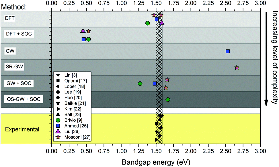 | ||
| Fig. 1 Comparison of the reported experimental bandgaps of MAPbI3 (obtained by absorption spectroscopy,17–19 diffuse reflectance spectroscopy,20–22 device stack ellipsometry23) from both experimental studies3,17–24 and first principles calculations.9,25–27 The hatched area that encompasses the black markers corresponds to the spread of experimental values (∼0.1 eV). The coloured markers show the position of calculated bandgaps from various ab initio studies (the type of method is specified on the left). SRGW stands for scalar relativistic GW.27 | ||
The ab initio methods used to calculate the energy band diagram of MAPbI3 generally divide into density-based and Green's function based schemes (Fig. 1). Inexpensive density- based implementations such as local-density approximation (LDA),4,5 semi-local generalized gradient approximations (GGA)6 and PBE (Perdew–Burke–Ernzerhof functional)7 give a fortuitously good fundamental gap by neglecting spin–orbit coupling (SOC). However, it was realized that this good agreement results from a cancellation of errors,8,9 spin–orbit interactions (SOC) are in fact of foremost importance to the optoelectronic properties of the material – they account for up to 1 eV to the 1.6 eV bandgap of the Pb-based perovskites.10 Implementing SOC significantly modifies band dispersions.9
Approaches using non-localised hybrid functionals that replace approximately 25% of DFT exchange with Hartree-Fock, improve on the LDA. The gap may be tuned with a judicious choice of parameters; however the choice of functional (e.g. the amount of Hartree-Fock to admix) is unclear for relatively new compounds, yet it might have a significant influence on band dispersions.
By contrast, Green's function methods, and the GW approximation in particular, are designed for excited state properties, and provide a systematically better approach to calculate quasiparticle levels. GW yields a good bandgap for MAPbI3, though there is some discrepancy among different approaches to GW. This is in part because implementations are usually LDA based (meaning G and W are calculated from DFT). Quasiparticle self-consistency in the GW context (QSGW) removes all arbitrariness from the ambiguity in the choice of the starting Hamiltonian.11,12 DFT-based GW results in a significantly narrower band gap relative to self-consistent GW. This point is often overlooked, because an additional approximation, namely the pseudo-potential approximation is widely used. It tends to overestimate gaps; when used in conjunction with DFT as a starting Hamiltonian, the two errors tend to cancel one another,13 resulting in fortuitously good gaps. Moreover, errors are not systematic: the GW-LDA gaps in CuInSe2,14 InN,15 and NiO,16 for example, are all a small fraction of actual bandgaps. QSGW is much better because, while it has a universal tendency to slightly overestimate gaps owing to ladder diagrams not included in the polarization operator, the errors are small and also highly systematic across the periodic table.12 We note however, that QSGW is a very computationally expensive method which, in practice, cannot be extended to a large number of atoms.
Obtaining a bandgap showing reasonable agreement with experimental findings does not guarantee that the band dispersion is meaningful. A comparison of all the main optical features in the visible spectrum, and not only the bandgap, is useful to assess the accuracy of any method applied to a new material and has not been yet reported for MAPbI3.
Additional complexity arises from MA+ being able to rotate,28–30 which has been speculated to have an influence on the electronic and photo-physical properties of MAPbX3.31 Molecular dynamics simulations published by Frost et al. suggest that MA+ can align along several different preferential orientations (corresponding to the C–N axis of the molecule pointing at faces, edges or corners of the cube formed by the surrounding lead atoms).32 Quasi-elastic neutron scattering measurements were shown to be compatible with MA+ reorientations between these alignments with an activation energy on the order of 10 meV.30,33
Here, detailed optical characterization of MAPbX3 single crystals is compared with QSGW theory to give insights into the optoelectronic properties. We show good agreement between ab initio QSGW simulations and single crystal ellipsometry in the spectral range containing all the visible optical transitions (1.2–5.5 eV). This enables the unambiguous assignment of the different optical features to their corresponding inter-band transition. QSGW is further used to determine the influence of cation orientation in the crystal on the optical properties of MAPbI3. Finally we use the optical data and calculations to help interpret the features of transient absorption spectra.
Methods
Sample preparation
Single crystals of MAPbX3 were synthetized from aqueous solution based on the method described by Poglitsch and Weber.28 The detailed procedure is given in the ESI Note S1.† Thin films of MAPbI3 with a mirror flat surface (rms roughness <10 nm see ref. 34) were prepared from a precursor solution in a DMSO/GBL mix using the toluene method,35 details of which are also given in Note S1.† Films of sufficient quality for ellipsometry were not produced for the other halides. A description of the MAPbI3 devices used for electroluminescence and sub-bandgap external quantum efficiency measurements can be found in the ESI Note S1.†Electroluminescence and sub-band gap external quantum efficiency
Electroluminescence (EL) was measured using a Shamrock 303 spectrograph combined with an iDUS InGaAs array detector cooled to −90 °C. EL from perovskite devices is measured at forward current densities between 1.25 and 1250 mA cm−2. The absorption coefficient is determined using the reciprocity relation between photovoltaic quantum efficiency (measured as described in the ESI Note S2†) and electroluminescent emission of solar cells, as described in ref. 36. The data was geometrically rescaled to line up on the ellipsometry data.Diffuse reflectance
Diffuse reflectance measurements were performed on MAPbX3 single crystals crushed into a fine powder. Details of the method can be found in the ESI (Note S3).†Ellipsometry measurements
Spectrometric ellipsometry measurement were performed at room temperature and low humidity (<30% RH). The data on thin films was gathered using a VASE-ellipsometer from J. A. Woollam Co., Inc. equipped with Autoretarder™. Optical spectra on thin films were recorded from ca. 0.9 eV to 4.2 eV, at five incidence angles for each sample (55°, 60°, 65°, 70°, 75°).Measurements on single crystals were performed with a SOPRALAB GES5E rotating polarizer ellipsometer mounted in a vertical configuration which is well suited for single crystals. The investigated photon energy range was from ca. 1.2 eV to 5.5 eV. Spectra were acquired at six incidence angles (55°, 60°, 65°, 67.5°, 70°, 75° for both MAPbI3 and MAPbBr3 and 55°, 60°, 62.5°, 65°, 70°, 75° for MAPbCl3).
Ellipsometry fitting
Ellipsometric optical spectra are analysed using the WVASE 32 software from J. A. Woollam Co., Inc. for thin films and Winelli2 from SOPRALAB for single crystals. To fit the experimental data, an initial model of the optical transitions is built for each material constituting the sample. Any contribution other than the optical transitions is assumed to be negligible. It is apparent from eqn (1), which gives the functional form of the joint density of states (jDOS) for doubly degenerate conduction and valence band (strictly valid only for centrosymmetric crystals37), that points of reciprocal space (crystal momentum, k) for which valence and conduction band (with energies Ev and Ec) are close to parallel will substantially contribute to jDOS as the denominator in the integral will tend to zero:37 | (1) |
 | (2) |
Analysing the dimensionality of the critical points
The dimensionality of the CPs is determined by fitting the second derivative of the dielectric function. This method enables the background to be removed during the fit as well as the accurate assessment of the dimensionality of the CPs. The fitted expression is therefore:38 | (3) |
Ab initio relativistic quasi-particle self-consistent GW calculation
The band structure discussed here is calculated from the quasiparticle self-consistent GW theory12 (QSGW) implemented in an all-electron framework.11 The QSGW procedure captures many-body effects and casts them optimally in an effective non-interacting Hamiltonian. Self-consistency is crucial for calculations on new materials, as it removes any ambiguity related to starting-point dependence that is problematic for the various kinds of one-shot GW implementations. Its absence has been shown to be a significant source of error for other semiconductors.12The crystal structures were optimized with the PBEsol functional using the VASP package as previously reported.7,39 Separate calculations are performed for the three local equilibrium alignments of MA C–N bonds: parallel to <100> (face), <110> (edge) and <111> (diagonal).32 They provide a complete set of data for the study the impact of cation orientation on the optical properties.
The QSGW self-energy is generated using a 3 × 3 × 3 k-mesh. A one-shot calculation was carried out for a 4 × 4 × 4 k-mesh, as a perturbation to the QSGW result for the 3 × 3 × 3 case and found to increase the gap by 0.2 eV. Thus our results slightly underestimate the converged QSGW band gap. QSGW tends to overestimate the band gap by slightly more than 0.2 eV, and thus a slight overestimate relative to the experimental band gap is expected here.
Optical calculations
Given a self-consistent QSGW potential, one can calculate the optical properties from the polarizability obtained using the random phase approximation (RPA) on a 14 × 14 × 14 k-mesh – for sufficient resolution. The non-interacting polarization P(q, ω) for reciprocal space vector q and excitation angular momentum ω is calculated as a sum of independent particle-hole contributions; and the inverse dielectric function is obtained from ε−1 = [1 − ν(q)P(q,ω)]−1 where ν(q) is the bare Coulomb interaction. The macroscopic dielectric function εM is: | (4) |
Given v and P, it is straightforward to calculate εM. In this all-electron implementation, Im(P(q,ω)) is calculated for a small q using eqn (40) of ref 11 while the real part can be obtained through Kronig-Kramers relation.40
We assumed that the MA ions are oriented along the three equilibrium directions (parallel to <100> (face), <110> (edge) and <111> (diagonal)) which are degenerate because of crystal symmetry. Given a particular orientation of MA, effective n and κ values are obtained by averaging the results obtained in the three directions of space. To obtained the optical constants of the material, a weighted average of n and κ is calculated using the orientational probabilities from ref. 32.
Simulation of transient absorption (TAS) spectra
Transient absorption spectroscopy (TAS) measures the change in optical absorption of a material between an initial state without any excited electrons and a secondary state where a number of electrons (holes) have been excited to the conduction (valence) band after varying relaxation times. To simulate TAS the imaginary part of the dielectric function was initially calculated using: | (5) |
 | (6) |
To obtain the simulated TAS spectra presented in the results and ESI,† the DOS was calculated on a 120 × 120 × 120 k-mesh which enabled accurate calculations related to the number of electron (holes) in the conduction (valence) bands. The Optical calculations were performed on a 30 × 30 × 30 mesh as this provided sufficient resolution for the purposes of this calculation. Assuming a value for the photo-excited carrier density, the quasi-Fermi levels can be calculated for a given temperature. The equilibrium state absorption spectrum was calculated using the same method by having the quasi-Fermi level of both carrier species at middle of the band-gap, while for the excited spectrum, quasi-Fermi levels associated with carrier density at room temperature were utilised.
Empirically it was found that rescaling the calculated energy axis according to hν → 0.653 hν + 0.608 gives an excellent match between the peak position obtained by ellipsometry and those from QSGW (see Fig. S1 in the ESI†). This transformation was applied to TAS before converting to wavelength to get a better match with experiments.
Results and discussion
Measured optical properties
Fig. 2 shows the optical constants n and κ (index of refraction and extinction coefficient, respectively) for MAPbI3, MAPbBr3 and MAPbCl3 determined from spectroscopic ellipsometry of the surface of single crystals (SCs) and a thin film (TF) in the case of MAPbI3. They were determined by fitting a model based on critical points (CPs) of the joint density of state (jDOS).37,41 CPs were used in preference to a harmonic oscillator model because they allow a more meaningful physical interpretation (discussed further below and in the ESI Note S6†). An ensemble of four CPs was sufficient to describe the optical response of MAPbI3 accurately on the range 1.2 to 5.5 eV (a fifth is used to account for the background). Only four and three CPs were required to model MAPbBr3 and MAPbCl3 respectively within the measured range (1.2–5.5 eV). The fits of SC (and TF) ellipsometry data at different angles of incidence are given ESI (Fig. S2–S5†) for the three halide types; together with their respective CP models (Tables S1–S4†). | ||
| Fig. 2 Optical constants (extinction coefficient (a, c, e) and index of refraction (b, d, f)) of CH3NH3PbI3 (a and b), CH3NH3PbBr3 (c and d) and CH3NH3PbCl3 (e and f) derived from single crystal ellipsometry (solid blue lines), thin film CH3NH3PbI3 (dashed green lines) and theory (chained orange lines, see Methods section). The three main optical features of CH3NH3PbI3 are assigned to the appropriate inter-band transition (VB and CB stand for ‘valence band’ and ‘conduction band’, respectively. The subscripts ‘1’ and ‘2’ correspond to the highest (lowest) VB (CB) or second highest (lowest) VB (CB)). The subscripts outside the brackets designate the symmetry point where the transition occurs in the first Brillouin zone, as defined in Fig. 4. | ||
The optical constants derived for thin films are comparable to those obtained for single crystals. The discrepancies are attributed to the differences in microscopic structure and orientation, and possible differences in the material's density. There may also be differences in scattering induced depolarization which cannot be analysed with our setup as we are not measuring the full Mueller Matrix.
Varying angle spectroscopic ellipsometry is often not sufficiently accurate to determine the absorption coefficient near the band edge. In b we use a combination of electroluminescence and diffuse powder reflectance to investigate the spectral region near the fundamental transition. A very sharp absorption edge is apparent for all materials, consistent with previous reports for MAPbI3![[thin space (1/6-em)]](https://www.rsc.org/images/entities/char_2009.gif) 21 and MAPbBr3.42 The values show good quantitative agreement with optical constants of thin MAPbI3 films published by Löper et al.18 but differ from other reports3 where the values may be influenced by parasitic scattering and the presence of PbI2.
21 and MAPbBr3.42 The values show good quantitative agreement with optical constants of thin MAPbI3 films published by Löper et al.18 but differ from other reports3 where the values may be influenced by parasitic scattering and the presence of PbI2.
Comparison between the different halide types
Fig. 2 shows that substituting iodide by lighter halides increases the bandgap of the compound from ∼1.55 (I) to 2.24 (Br) to 2.97 (Cl) eV (see the Tauc plots assuming direct band gap transitions obtained from diffuse reflectance measurements in Fig. 3 insets). Three main absorption peaks (corresponding to CPs) can be observed in MAPbI3 at 1.6, 2.5 and 3.1 eV. In MAPbBr3 three peaks can also be seen at ∼2.3, 3.5 and 4.5 eV. MAPbCl3 shows only two peaks within the measured range, at ∼3.1 and 4.6 eV (a third peak ∼5.6 eV can be distinguished slightly out of the confidence range). The absorption peak near the band gap increases in amplitude for lighter halides, as indicated by the blue arrows in Fig. 2. This behaviour is likely to be due to excitonic absorption as will be discussed further below. | ||
| Fig. 3 Absorption coefficient (α = 4πκ/λ, where λ is the wavelength) for the three compounds (a. MAPbI3, b. MAPbBr3 and c. MAPbCl3) determined by a combination of techniques: single crystal ellipsometry (solid blue line), diffuse reflectance spectroscopy (solid orange line) using single crystals crushed to a powder and electroluminescence on devices for MAPbI3 (solid green line). Detail of the device architecture is given in Note S1 in the ESI.† The lines are dotted in the energy regions outside the instrument measurement capabilities. The slopes of d[hν]/d[log10(α)] are given in the picture in a colour matching the corresponding curves. Tauc plots derived from the diffuse reflectance data are given as insets together with the estimated value of the bandgap. | ||
Assignment of the optical transitions
In the discussion that follows the energy bands above the band gap are referred to as CB1, CB2, ⋯, and the energy bands below the band gap are referred to as VB1, VB2,… (see labels in Fig. 4a). A comparison between the optical constants of MAPbI3 calculated from QSGW (orange dotted line) and those obtained by ellipsometry (solid blue line) is presented in Fig. 2a and 2b. Qualitatively, both the shape and amplitude of the calculated spectra of n and κ show good agreement with experimental findings. QSGW was performed on the pseudo cubic perovskite phase. This gives a good approximation of the band structure since the transition from the tetragonal to the pseudo-cubic phase is a second order transition (unlike the 1st order orthorombic to tetragonal transition) which results in only a 2% change in the lattice parameters relative to the tetragonal structure at room temperature.33 Thus we expect little effect of this approximation on the calculated optical constants. The predicted bandgap energy is 1.62 eV, close to the 1.5–1.6 eV obtained experimentally without the introduction of any empirical parameter. The computed and experimental extinction coefficient spectra show the same number of features in the visible spectral range. The features in the theoretical spectra are less well resolved than their experimental counterparts because the optical properties calculated for different cation alignments have been averaged and also due to the absence of electron–hole interactions in calculations as discussed below and in the Methods section. (The calculated optical constants are plotted over a larger energy range (1–10 eV) in the ESI, Fig. S6,† where each material shows the same qualitative features progressively blue shifted with decreasing radii of halide ions.) The calculated optical constants for each material also show a non-linear blue shift of the optical features relative to the experimental values – a ‘stretching’ of the curves towards higher energies. We attribute this phenomenon to the use of Random Phase Approximation (RPA) which does not account for electron–hole interactions. A better match between theory and experiment would be achieved by adding ladder diagrams to the RPA bubbles.43 The additional diagrams are thought to only slightly reduce the self-energy, but they have a more pronounced effect on the dielectric function, as electron–hole pairs get attracted through the screened coulomb interaction W. This is discussed by Louie and Rohlfing in ref. 44. They show that the blue shift resulting from the omission of electron–hole interactions in GW can exceed 0.5 eV in the case of Si, while it is as high as a few eV for LiF. Unfortunately, the addition of ladder diagrams via a Bethe-Salpeter equation has not yet been achieved in the all-electron QSGW framework. We note that contribution of surface effects could also account for some of the observed discrepancies between observation and calculation, although we believe ignoring their effects to be less significant than the error made by using the RPA. | ||
| Fig. 4 a. Energy band diagram of MAPbI3 along the relevant k-branches in the first Brillouin zone. The labels tag the critical point transitions with the appropriate inter-band transitions (see Fig. 2) b. Schematic representation of the first Brillouin zone showing the position of the high symmetry points used in a. and c. c. Difference between conduction and valence band energy plotted for relevant band pairs. The colour code is the same as given in the inset to d. d. Imaginary part of the dielectric function (Im(ε)). The colour code helps visualizing the contributions of the different transition to Im(ε). The area filled in dark red shows the small contribution to the imaginary part of the dielectric function from other transitions than VB1 to CB1. The lines between c and d underline the correspondence between the extrema of Ec − Ev and the points of high absorption (see eqn (1) in the Methods section). e. Simulated transient absorption spectrum for a charge carrier density of 10−5 per unit cell (4 × 1016 cm−3). The dashed black line corresponds to the summed contribution of all transitions and rescaled according to the procedure detailed in the Methods section. The main individual contributions are shown (solid coloured lines). ‘PB1’ and ‘PB2’ label the two photo-bleaches. The inset shows schematic band diagrams and optical transitions for three different scenarios: (i) no photo-excited population, (ii) photo-excited population following a pulse with energy greater than 2.6 eV (477 nm) and (iii) after excitation with a pulse energy between 1.6 and 2.5 eV (780 and 500 nm) or following relaxation of photo-excited population from (ii) within the CBs and VBs. | ||
With this expected discrepancy taken into account, the quality of the agreement enables the unambiguous assignment of the three main optical features (labels in Fig. 2a and b) to their corresponding inter-band excitations. Fig. 4a shows the energy band diagram derived from QSGW calculations9 along the relevant k-branches defined on Fig. 4b. The energy difference between conduction and valence band is plotted in Fig. 4c for different band pairs. Extrema of the curves in reciprocal space, where the conduction and valence band energies are close to parallel, correspond to CPs of the joint density of states (see eqn (1) in the Methods section). The joint density of states is the number of electronic states per unit energy and volume in the conduction and valence bands that are separated by a given photon energy taking into account spin degeneracy and selection rules. Points where the conduction and valence bands track each other (i.e. where the gradient ∇k(Ec − Ev) is minimal) dominate the dielectric function. This is replotted in Fig. 4d together with the relative contribution from different inter-band transitions.
Inspection of Fig. 2a and 4a–d show the striking result that transitions between the highest valence band, VB1, and the lowest conduction band, CB1, are responsible for almost all the optical properties in the visible spectral range. The ellipsometry CP at the bandgap (1.62 eV, see Table S1†) is due to the inter-band transition VB1 to CB1 at the R symmetry point in the first Brillouin zone (Fig. 4b). Similarly, the second feature (modelled with a CP at 2.48 eV) involves the transition from VB1 to CB1 at the M point (with a very minor contribution from VB1 to CB2 at the R point), while the third feature (modelled with a CP at 3.08 eV) is due to the promotion of electrons from VB1 to CB1 at the X point and also contributions from VB1 to CB2 and VB2 to CB1 around the M symmetry point. A similar band structure is obtained for Br- and Cl-based perovskite, as shown in Fig. S7 in the ESI.†
The sharp absorption feature observed at the band edge in all three materials may result from a discrete excitonic state enhancing absorption in this region. We reiterate that the electron–hole interaction is not accounted for in QSGW and thus cannot reproduce this feature. This may account for the much weaker computed absorption onset around 1.6 eV. The discrepancies between optical constants determined by ellipsometry compared to the modelled ones are larger for lighter halides. This larger error is consistent with the observed increased excitonic nature of the compounds, which indicates a larger contribution of electron hole coupling on the optoelectronic properties of the compounds. Similarly the increasingly excitonic nature of the absorption edge for light halide is expected to increase the discrepancies between ellipsometry and diffuse powder reflectance results (see Fig. 3). In our ellipsometry model, the bandgap feature is modelled by one critical point only (to avoid parameter cross-correlation) whereas, physically, two features are superimposed (the onset of the joint density of states and the excitonic peak). Fitting a CP to ellipsometry data of a prominent excitonic peak at the band edge will often result in the slope of the modelled extinction coefficient vs. energy being steeper than in reality. This partly explains the discrepancy between the ellipsometry and diffuse reflectance measurements, additional contributions to the discrepancy are also likely to result from the change in sample morphology and surface properties when grinding the SCs to a powder.
Properties and dimensionality of the critical points
The second derivative of the dielectric function provides insight into the dimensionality of the critical points (cf. Method section). The d2ε/dE2 of the three MAPbX3 compounds was best fit by CPs corresponding to 0D transitions (Fig. S8–S10 and Tables S5–S7†). 0D transitions are often a characteristic of localized excitations. 0D CPs are also obtained in the case of dispersionless electron–hole states (i.e. where dE/dk ≈ 0). This is the case when the effective mass of both electron and hole are large (and the mobilities low since they are inversely proportional to d2E/dk2) at a transition k-point.The band structure in Fig. 4a shows that the bottom of the conduction band has a low curvature. This is partly because the band around the R point is split due to spin orbit coupling (sometimes called ‘Rashba-splitting’) resulting in a flat and non-parabolic effective dispersion.45 Thus the calculated band structure is consistent with the use of a 0D critical point ellipsometry model. This observation emphasises the importance of accounting for spin–orbit coupling on the band structure dispersion of MAPbI3.
Interpretation of transient absorption spectra
The contribution of different CB and VB and valence band pairs to the optical properties can be used to simulate transient absorption spectrum (TAS) of the material. This is achieved by calculating the difference in extinction coefficient between the semiconductor in its ground state and the case where the conduction and valence band have been respectively populated with electrons and holes from an optical pulse. The photoelectrons and holes are assumed to be thermally relaxed within their respective bands into a Fermi–Dirac distribution with a quasi-Fermi level. Fig. 4e shows a simulated transient absorption spectrum and the relative contributions from different optical transitions for an electron density of 10−5 per unit cell. It is calculated from the band-pair contributions to the density of states convolved with the Fermi–Dirac distributions multiplied by the corresponding optical matrix elements. To allow comparison with experiment we have shifted the energies of the transitions to correspond to the experimental wavelengths they were assigned to (see Methods section).The simulated spectrum shows bleaching features at around 720 nm and 460 to 480 nm. These are likely to correspond to the main photo-bleach features observed experimentally at 760 nm and 480 nm.46,47 Our calculations suggest that the low energy bleach is exclusively due to the population photo-generated charges in VB1 and CB1 at the R point. The second bleach at higher energy is likely to be due to a combination of inter-band transitions involving the VB1 to CB2, VB2 to CB1 and VB1 to CB3 in proportions that vary depending on the density of photogenerated charge carriers (see Fig. S11 in the ESI†). This also implies that the relative magnitude of the bleach signal PB2 will be greater immediately following a short wavelength excitation pulse (∼400 nm) compared to excitation with a longer wavelength pulse close to the band gap. This is because directly after excitation with short wavelengths, PB2 will have contributions from both the depletion of the electronic states at the top of VB1 and VB2 and by the filling of CB1, CB2 and CB3 (case ii in Fig. 4e). Thermalization of photo-excited electrons from CB3 and CB2 to CB1, and photo-excited holes from VB2 to VB1 will then occur on a picosecond timescale (case iii in Fig. 4e). The magnitude of PB2 will therefore be reduced since bleaching will arise solely from the filling of CB1 and depletion of VB1. Consequently thermalization is expected to strengthen PB1 relative to PB2. Our calculations show that significant contributions to PB2 from VB1 to CB2 and CB3 transitions are likely in addition to the VB2 to CB1 transition that has been hypothesised previously to explain the interpretation of experimental TAS spectra.46–49
The photoinduced absorption commonly measured in MAPbI3 between the main photo-bleaches is not reproduced by our approach. This effect might therefore be due to (i) relaxation of the structure after excitation of a charge carrier to the CB, for example local reorientation of methylammonium cation to screen the charge that was transferred from I to Pb orbitals and/or (ii) the Stark effect.
The influence of MA+ orientation on the optical properties
We now compare the optical properties of MAPbI3 for the three isotropic MA+ equilibrium alignments. They correspond to MA+ pointing at the face of the cube formed by the surrounding lead atoms (direction <100>, Fig. 5a), or pointing at edges (direction <110>, Fig. 5b), or along the diagonal (direction <111>, Fig. 5c).32,39 In the absence of electric field or any significant interaction between the MA+, the orientational distribution determined by Frost et al.32 is 42% along <100>, 31% along <110> and 26% along <111>.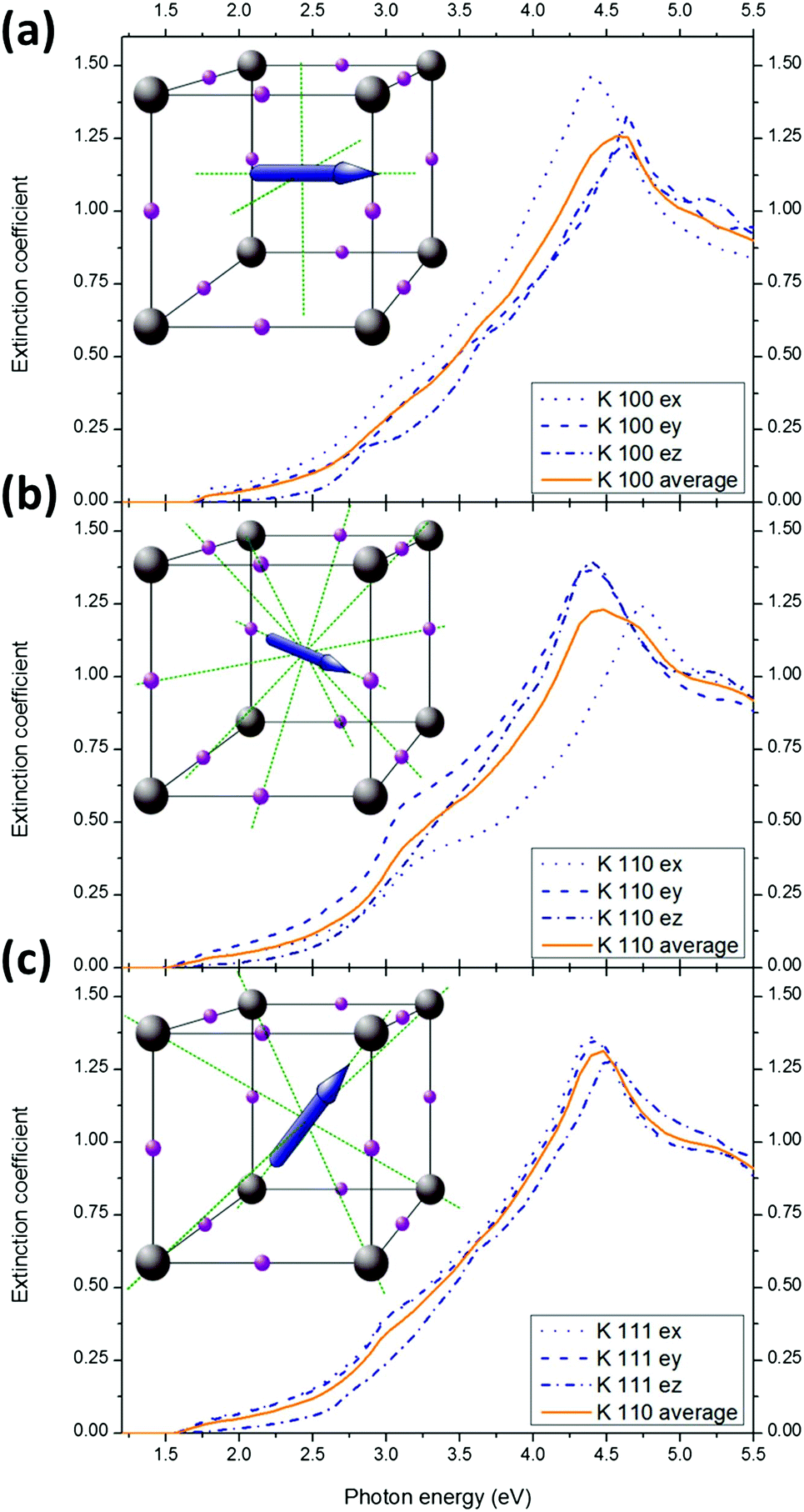 | ||
| Fig. 5 Anisotropy of calculated optical constants for the three equilibrium orientations: for MA+ pointing at the faces (a), at the edges (b) and at the corners (c). An inset diagram shows one of possible orientation (blue arrow) among a set of equivalent alignments (dashed green lines). | ||
The general aspect of the extinction coefficient (averaged in the directions of space) corresponding to the different orientations shows a similar shape over the investigated range (1.2–5.5 eV). However, some subtle variations are of importance. Especially, different bandgaps are expected for different orientations: 1.60 eV for the <100> orientation (pointing at faces), 1.46 eV for the <110> (pointing at edges) and 1.52 eV in <111> (pointing at corners). This result suggests that collective orientation of the dipoles in a preferential direction would result in different local bandgaps. If, as suggested previously, ferroelectric (or polarized) domains can indeed form in perovskite layers,32,50–52 local variation of the optical constants are expected. The application of a sufficient electric field is therefore expected to modify the bandgap within a single crystal (or a grain). Moreover, in case of local preferential orientation, the difference between the optical constants in the three spatial directions Fig. 5a–c will result in significant local anisotropy. The optical constants along the three directions of space in case of preferential alignment are given for MAPbBr3 and MAPbCl3 in the ESI Fig. S12 and S13.†
However, MA+ alignment is unlikely to explain the experimental variations of the measured bandgaps in literature for MAPbI3 as all of these techniques probe the macroscopic optical constants and not on the sub ∼100 nm scale. The orientation of the grains is believed to be random in most cases53,54 so that even when an electrical bias is applied, the macroscopic optical constants would be an average of the dominant orientations. We believe that much of the variation in the reported experimental band gaps result from differences in the details of the sample preparation, measurements and analysis.
Conclusions
In conclusion, we have presented a precise derivation of the optical constants of MAPbI3, MAPbBr3, and MAPbCl3 from single crystal varying angle spectroscopic ellipsometry on the visible part of the spectral range as well as further measurements of the optical absorption and emission of films and powders. The good agreement obtained between experimental optical constants of MAPbI3 and the one derived from QSGW in the 1.2–5.5 eV range allows the unambiguous assignment of the optical features to inter-band transitions. We showed that the optical response of MAPbI3 is dominated by the transition between the highest valence band the lowest conduction band, and that the contribution of other transitions is minimal due to small optical matrix elements. We have used the calculated band structure informed by our optical measurements to explain the origin of the photo-bleaching features that have been observed in transient absorption spectra. While the low energy bleach (780 nm experimentally) in the TAS seems exclusively due to the population photo-generated charges in VB1 and CB1 at the R reciprocal point, the second bleach at higher energy (480 nm) can be understood as a combination of inter-band transitions involving the VB1 to CB2, VB2 to CB1 and VB1 to CB3 in proportions that vary depending on the density of photogenerated charge carriers. Previously only VB2 to CB1 were suggested to contribute to this bleaching. Decomposition of the QSGW results for different cation orientations shows significant differences suggesting that local preferential orientation would lead to sizeable variations of the optical properties.Acknowledgements
We thank Jarvist M. Frost and Paul N. Stavrinou for useful discussions, Xiao Li for assistance with sample preparation and Stefan A. Maier for access to equipment. PB and AL are grateful to the EPSRC (EP/J002305/1, EP/M014797/1 and EP/M023532/1) for financial support. JN thanks the EPSRC for funding (EP/J017361 and EP/K030671/1). MCQ and MIA acknowledge financial support from MINECO through project MAT2012-37776. The theory portion of this work was supported by EPSRC (EP/M009602/1, EP/K016288/1 and EP/M009580/1).References
- W. Shockley and H. J. Queisser, J. Appl. Phys., 1961, 32, 510–519 CrossRef CAS.
- C. Roldan-Carmona, O. Malinkiewicz, R. Betancur, G. Longo, C. Momblona, F. Jaramillo, L. Camacho and H. J. Bolink, Energy Environ. Sci., 2014, 7, 2968–2973 CAS.
- Q. Lin, A. Armin, R. C. R. Nagiri, P. Burn and P. Meredith, Nat. Photonics, 2015, 9, 106–112 CrossRef CAS.
- P. Hohenberg and W. Kohn, Phys. Rev., 1964, 136, B864 CrossRef.
- W. Kohn and L. J. Sham, Phys. Rev., 1965, 140, A1133 CrossRef.
- J. P. Perdew, J. A. Chevary, S. H. Vosko, K. A. Jackson, M. R. Pederson, D. J. Singh and C. Fiolhais, Phys. Rev. B: Condens. Matter, 1992, 46, 6671 CrossRef CAS.
- J. P. Perdew, A. Ruzsinszky, G. a. I. Csonka, O. A. Vydrov, G. E. Scuseria, L. A. Constantin, X. Zhou and K. Burke, Phys. Rev. Lett., 2008, 100, 136406 CrossRef PubMed.
- E. Mosconi, A. Amat, M. K. Nazeeruddin, M. Graetzel and F. De Angelis, J. Phys. Chem. C, 2013, 117, 13902–13913 CAS.
- F. Brivio, K. T. Butler, A. Walsh and M. van Schilfgaarde, Phys. Rev. B: Condens. Matter, 2014, 89, 155204 CrossRef.
- D. A. Egger and L. Kronik, J. Phys. Chem. Lett., 2014, 5, 2728–2733 CrossRef CAS PubMed.
- T. Kotani, M. van Schilfgaarde and S. V. Faleev, Phys. Rev. B: Condens. Matter, 2007, 76, 165106 CrossRef.
- M. van Schilfgaarde, T. Kotani and S. Faleev, Phys. Rev. Lett., 2006, 96, 226402 CrossRef CAS PubMed.
- E. L. Shirley, X. Zhu and S. G. Louie, Phys. Rev. B: Condens. Matter, 1997, 56, 6648–6661 CrossRef CAS.
- J. Vidal, S. Botti, P. Olsson, J.-F. Guillemoles and L. Reining, Phys. Rev. Lett., 2010, 104, 056401 CrossRef PubMed.
- M. Usuda, N. Hamada, K. Shiraishi and A. Oshiyama, Jpn. J. Appl. Phys., 2004, 43, L407 CrossRef CAS.
- S. V. Faleev, M. van Schilfgaarde and T. Kotani, Phys. Rev. Lett., 2004, 93, 126406 CrossRef PubMed.
- Y. Ogomi, A. Morita, S. Tsukamoto, T. Saitho, N. Fujikawa, Q. Shen, T. Toyoda, K. Yoshino, S. S. Pandey, T. Ma and S. Hayase, J. Phys. Chem. Lett., 2014, 5, 1004–1011 CrossRef CAS PubMed.
- P. Löper, M. Stuckelberger, B. Niesen, J. Werner, M. Filipic, S.-J. Moon, J.-H. Yum, M. Topic, S. De Wolf and C. Ballif, J. Phys. Chem. Lett., 2015, 6, 66–71 CrossRef PubMed.
- M. M. Lee, J. Teuscher, T. Miyasaka, T. N. Murakami and H. J. Snaith, Science, 2012, 338, 643–647 CrossRef CAS PubMed.
- F. Hao, C. C. Stoumpos, Z. Liu, R. P. H. Chang and M. G. Kanatzidis, J. Am. Chem. Soc., 2014, 136, 16411–16419 CrossRef CAS PubMed.
- T. Baikie, Y. Fang, J. M. Kadro, M. Schreyer, F. Wei, S. G. Mhaisalkar, M. Graetzel and T. J. White, J. Mater. Chem. A, 2013, 1, 5628–5641 CAS.
- H.-S. Kim, C.-R. Lee, J.-H. Im, K.-B. Lee, T. Moehl, A. Marchioro, S.-J. Moon, R. Humphry-Baker, J.-H. Yum, J. E. Moser, M. Graetzel and N.-G. Park, Sci. Rep., 2012, 2, 591 Search PubMed.
- J. M. Ball, S. D. Stranks, M. T. Horantner, S. Huttner, W. Zhang, E. J. W. Crossland, I. Ramirez, M. Riede, M. B. Johnston, R. H. Friend and H. J. Snaith, Energy Environ. Sci., 2015, 8, 602–609 CAS.
- J. M. Ball, M. M. Lee, A. Hey and H. J. Snaith, Environ. Sci., 2013, 6, 1739 CAS.
- T. Ahmed, C. La-O-Vorakiat, T. Salim, Y. M. Lam, E. E. M. Chia and J.-X. Zhu, EPL, 2014, 108, 67015 CrossRef.
- S. Liu, F. Zheng, N. Z. Koocher, H. Takenaka, F. Wang and A. M. Rappe, J. Phys. Chem. Lett., 2015, 6, 693–699 CrossRef CAS PubMed.
- E. Mosconi, P. Umari and F. De Angelis, J. Mater. Chem. A, 2015, 3, 9208–9215 CAS.
- A. Poglitsch and D. Weber, J. Chem. Phys., 1987, 87, 6373–6378 CrossRef CAS.
- R. E. Wasylishen, O. Knop and J. B. Macdonald, Solid State Commun., 1985, 56, 581–582 CrossRef CAS.
- A. M. A. Leguy, J. M. Frost, A. P. McMahon, V. G. Sakai, W. Kochelmann, C. Law, X. Li, F. Foglia, A. Walsh, B. C. O'Regan, J. Nelson, J. T. Cabral and P. R. F. Barnes, Nat. Commun., 2015, 6, 7124 CrossRef PubMed.
- J. Even, L. Pedesseau and C. Katan, Phys. Chem. C, 2014, 118, 11566–11572 CrossRef CAS.
- J. M. Frost, K. T. Butler and A. Walsh, APL Mater., 2014, 2, 081506–081516 CrossRef.
- M. T. Weller, O. J. Weber, P. F. Henry, A. M. Di Pumpo and T. C. Hansen, Chem. Commun., 2015, 51, 4180–4183 RSC.
- A. M. A. Leguy, Y. Hu, M. Campoy-Quiles, M. I. Alonso, O. J. Weber, P. Azarhoosh, M. van Schilfgaarde, M. T. Weller, T. Bein, J. Nelson, P. Docampo and P. R. F. Barnes, Chem. Mater., 2015, 27, 3397–3407 CrossRef CAS.
- Z. Xiao, Q. Dong, C. Bi, Y. Shao, Y. Yuan and J. Huang, Adv. Mater., 2014, 26, 6503–6509 CrossRef CAS PubMed.
- U. Rau, Phys. Rev. B: Condens. Matter, 2007, 76, 085303 CrossRef.
- P. Y. Yu and M. Cardona, Fundamentals of Semiconductors, Springer-Verlag, 2001 Search PubMed.
- P. Lautenschlager, M. Garriga, S. Logothetidis and M. Cardona, Phys. Rev. B: Condens. Matter, 1987, 35, 9174–9189 CrossRef CAS.
- F. Brivio, A. B. Walker and A. Walsh, Appl. Phys. Lett., 2013, 1, 042111 Search PubMed.
- R. d. L. Kronig, J. Opt. Soc. Am., 1926, 12, 547–556 CrossRef CAS.
- M. Campoy-Quiles, J. Nelson, D. D. C. Bradley and P. G. Etchegoin, Phys. Rev. B: Condens. Matter, 2007, 76, 235206 CrossRef.
- E. Edri, S. Kirmayer, D. Cahen and G. Hodes, J. Phys. Chem. Lett., 2013, 4, 897–902 CrossRef CAS PubMed.
- E. E. Salpeter and H. A. Bethe, Phys. Rev., 1951, 84, 1232–1242 CrossRef.
- M. Rohlfing and S. G. Louie, Phys. Rev. B: Condens. Matter, 2000, 62, 4927–4944 CrossRef CAS.
- F. Zheng, L. Z. Tan and A. M. Rappe, arXiv, 2015.
- J. A. Christians, J. S. Manser and P. V. Kamat, J. Phys. Chem. Lett., 2015, 6, 2086–2095 CrossRef CAS PubMed.
- J. S. Manser and P. V. Kamat, Nat. Photonics, 2014, 8, 737–743 CrossRef CAS.
- G. Xing, N. Mathews, S. Sun, S. S. Lim, Y. M. Lam, M. Grätzel, S. Mhaisalkar and T. C. Sum, Science, 2013, 342, 344–347 CrossRef CAS PubMed.
- S. D. Stranks, G. E. Eperon, G. Grancini, C. Menelaou, M. J. P. Alcocer, T. Leijtens, L. M. Herz, A. Petrozza and H. J. Snaith, Science, 2013, 342, 341–344 CrossRef CAS PubMed.
- Y. Kutes, L. Ye, Y. Zhou, S. Pang, B. D. Huey and N. P. Padture, J. Phys. Chem. Lett., 2014, 5, 3335–3339 CrossRef CAS PubMed.
- C. C. Stoumpos, C. D. Malliakas and M. G. Kanatzidis, Inorg. Chem., 2013, 52, 9019–9038 CrossRef CAS PubMed.
- H.-S. Kim, S. K. Kim, B. J. Kim, K.-S. Shin, M. K. Gupta, H. S. Jung, S.-W. Kim and N.-G. Park, J. Phys. Chem. Lett., 2015, 6, 1729–1735 CrossRef CAS PubMed.
- Y. Li, J. K. Cooper, R. Buonsanti, C. Giannini, Y. Liu, F. M. Toma and I. D. Sharp, J. Phys. Chem. Lett., 2015, 6, 493–499 CrossRef CAS PubMed.
- T. S. Williams, F. Zuo, C.-C. Chueh, C.-Y. Liao, P.-W. Liang and A. K.-Y. Jen, ACS Nano, 2014, 8, 10640–10654 CrossRef PubMed.
Footnotes |
| † Electronic supplementary information (ESI) available. See DOI: 10.1039/c5nr05435d |
| ‡ Both authors equally contributed to the work. |
| This journal is © The Royal Society of Chemistry 2016 |