
 Open Access Article
 This Open Access Article is licensed under a
 Creative Commons Attribution 3.0 Unported Licence
Titanium oxide nanoparticle dispersions in a liquid monomer and solid polymer resins prepared by sputtering†
Matteo
Porta
a,
Mai Thanh
Nguyen
a,
Tetsu
Yonezawa
*a,
Tomoharu
Tokunaga
b,
Yohei
Ishida
a,
Hiroki
Tsukamoto
a,
Yuichi
Shishino
c and
Yoshikiyo
Hatakeyama‡
d
aDivision of Materials Science and Engineering, Faculty of Engineering, Hokkaido University, Kita 13 Nishi 8, Kita-ku, Sapporo, Hokkaido 060-8628, Japan. E-mail: tetsu@eng.hokudai.ac.jp
bDepartment of Quantum Engineering, Graduate School of Engineering, Nagoya University, Furo-cho, Chikusa-ku, Nagoya, Aichi 464-8603, Japan
cTokai Optical, Co., Ltd., 5-26 Shimoda, Eta-cho, Okazaki, Aichi 444-2192, Japan
dDivision of Nanoscience, Graduate School of Advanced Integration Science, Chiba University, 1-33, Yayoi-cho, Inage-ku, Chiba 263-8522, Japan
First published on 16th September 2016
Abstract
A transparent resin containing titanium oxide nanoparticles (NPs) was prepared using a molten matrix sputtering (MMS) technique. The low vapour pressure of the liquid, pentaerythritol ethoxylate (PEEL) substrate permits the use of this vacuum technique directly with liquid PEEL under stirring conditions in order to obtain uniform dispersions of NPs. We found that it is possible to synthesize titanium oxide, TiOx, NPs with diameters of less than 5 nm with a controlled composition by simply adjusting the sputtering atmosphere. Furthermore, as the electronic structure of the TiOx NPs changes depending on the particle size, crystallinity and degree of oxidation, we were able to modify the optical properties of PEEL and the resin by embedding TiOx NPs in the matrix. The enhancement of the refractive index of a resin containing TiO2 NPs was also demonstrated. This synthetic method is promising for the advanced preparation of high purity TiOx NPs without using a reducing agent and leaving by-products for various applications in optical devices, energy conversion, and light harvesting in the UV visible region.
Introduction
Nanocomposite inorganic–organic hybrid materials, especially nanoparticles (NPs) embedded in polymers, have many promising applications in a broad range of fields with manipulated properties. NP-incorporated materials have been produced using various methods1–6 for different purposes.1,4,7–11 Chemical synthesis of NPs in matrices often uses toxic chemicals, leaves by-products, and requires an additional purification process, where dispersions of pre-formed NPs require additional dispersing agents to avoid agglomeration. The direct preparation of pure NPs that are well-dispersed in a matrix without using post-purification, therefore, is of considerable interest. In this context, modifying traditional sputtering techniques to generate and stabilize NPs in a liquid medium is one possible strategy to obtain pure NP-organic hybrid materials. This is possible with recent developments using highly viscous or low vapour-pressure liquids as substrates instead of solid ones. In light of this development, NP-hybrid materials synthesized via sputtering into liquid media (matrix sputtering techniques) have recently become an active research field. Using this method,12–26 robust NP size and composition control can be achieved in a single step process, such as the recently-reported synthesis of photo-luminescent metal NPs via sputtering in various liquid media.18–26Titanium dioxide, TiO2, NPs are important wide-bandgap materials used as UV-active photo-catalysts and various optical applications such as a UV block material in sunscreens, or to increase the refractive index of thin films7,26 and polymers.7,9 Modification of the electronic structure of TiO2via doping or introducing oxygen defects can narrow the bandgap and extend its energy harvesting applications towards the visible region.28 In addition, one stoichiometric oxide of titanium, TiO, with strong visible-light absorption can also be used for this purpose.28 The preparation of titanium oxides with control of its oxidation state offers a facile way to modify the optical properties of hybrid materials that contain titanium oxide NPs. Despite the fact that conventional chemical synthesis can produce TiO2 NPs, to the best of our knowledge very small (1–10 nm in diameter) and clean TiO2 NPs dispersed in polymers for use in advanced optical applications have not yet been reported. It is still a challenge to use chemical methods for synthesizing titanium oxides with controlled composition since the decomposition of titanium complexes can result in various undesired TiO2 phases. Finally, previously reported fabrications of hybrid films or polymers containing titanium or titanium oxide NPs featured multi-step processes that are complicated and often produce products with a greater presence of contaminations.4,7–9,27,29 With its many advantages over more traditional chemical synthesis in terms of purity and composition control with regards to the oxidation state, we posit that direct sputtering of Ti under controlled atmospheric conditions could be a valuable technique for the synthesis of titanium oxides. The composition of the sputtered material is strongly related to the atmosphere in the sputtering chamber, as reported by Dreesen et al.30 By controlling the oxygen flow rate into the sputtering chamber, they were able to sputter a film of metallic titanium and its oxides with low oxidation states when the O2 flow was below a certain threshold, but they otherwise sputtered titanium dioxide. This threshold was indicated by a change in the cathode voltage, which was constant at a high oxygen flow rate but diminished as the oxygen flow rate was decreased. This result suggests that the cathode voltage can be used as an indirect but a quantitative indicator for the atmosphere inside the sputtering chamber: a high oxygen atmosphere corresponds to the formation of TiO2, and the low oxygen one corresponds to the formation of titanium and titanium oxides with a lower oxidation state. In the present study, we introduced only Ar into the sputtering chamber after pump-purging, leading to a reduced oxygen content in the atmosphere inside the chamber with prolonged sputtering time. Based on monitoring the cathode voltage, we sputtered titanium in a high or low oxygen atmosphere and investigate the structural and optical properties of the obtained titanium oxide NPs dispersed in PEEL. We demonstrate the capability of our method to tailor the composition of titanium oxide NPs for the preparation of TiO NPs in PEEL with strong visible light absorption and nanocomposite resins containing monodispersed TiO2 NPs with an enhanced refractive index and high transparency.
Experimental
Materials
Pentaerythritol ethoxylate (3/4 EO/OH) (PEEL, C[CH2(OCH2CH2)nOH]4, Mn = 270) was purchased from Sigma-Aldrich. m-Xylylene diisocyanate (m-XDI) was purchased from TCI. The titanium 99.5% pure sputtering target (50 mm diameter, 3 mm thick) was purchased from Nilaco, Japan. All materials were used as received.Sputtering apparatus
A magnetron sputtering device was designed in order to be better suited for the synthesis of nanoparticles dispersed in liquid samples (Fig. S1, ESI†). A mechanical stirring device was installed in the sputtering chamber. A turbo molecular pump/oil rotary pump system and a gas purging system equipped to the sputtering device were used to control the vacuum level and the atmosphere inside the sputtering chamber. A cooling system was installed to avoid overheating of the target and a temperature control device was used to maintain the PEEL at a constant temperature during the experiments.Preparation of titanium oxide NPs dispersed in PEEL
PEEL was dried under vacuum at 125 °C in order to eliminate dissolved gases and volatile molecules. 2.5 g of PEEL were then placed in a glass Petri dish with an inner surface area of 5.7 cm2, and inserted in the sputtering chamber. The surface of the liquid PEEL was positioned 60 mm below the Ti sputtering target, and PEEL was stirred at a constant 60 rpm. At least 10 cycles of evacuation (up to ∼10−2 Pa) and injection of Ar gas (up to 2.0 Pa) were performed in the chamber. After this repeated purging and re-filling, the pressure of the chamber was then adjusted to 2.0 Pa with Ar flow and sputtering was initiated, generating and trapping the NPs in the liquid PEEL.During sputtering, Ar gas was introduced into the chamber in order to change the sputtering atmosphere. With sputtering time, the sputtering atmosphere varied as indicated by a change in the cathode voltage (Fig. 1) from 310 to 265 V, which corresponds to the colour of the plasma changing from blue to green. Hereafter, we use the colour (“blue” and “green”) of plasma to refer to the sputtering mode.
 | ||
| Fig. 1 Typical cathode voltage curve that accompanies the change between the two sputtering modes: blue-plasma sputtering on the left, and green-plasma sputtering on the right. | ||
The total sputtering time was modified for each sample from 1 to 3 h (divided in intervals in order to avoid extreme overheating of the sputtering target and to select the sputtering plasma conditions), with a sputtering current of 400 mA and the atmosphere inside the sputtering chamber was varied in order to control the oxidation states of the synthesized titanium oxide NPs. More detailed reaction conditions are summarized in Table 1.
Preparation of titanium oxide NPs embedded in a urethane resin
PEEL with dispersed TiO2 NPs and m-XDI were mixed under vacuum at a 1![[thin space (1/6-em)]](https://www.rsc.org/images/entities/char_2009.gif) :2 molar ratio. The polymerization occurred through the formation of urethane linkages:
:2 molar ratio. The polymerization occurred through the formation of urethane linkages:where R1 and R2 denoted the backbone of m-XDI and PEEL, respectively. We observed that without titanium oxides particles, much longer time was required for the polymerization to be complete. Probably, the TiO2 NPs acted as a catalyst and accelerated the polymerization.31 Because polymerization is an exothermic process, an increase in the reaction speed causes an increase in temperature. An ice bath was used to cool the reaction in order to prevent the formation of bubbles in the polymer. The liquid was then poured in a mould where it rapidly solidified, and was then heated in an oven for 6 h at a maximum temperature of 130 °C. After the polymers were cooled to room temperature, the final titanium oxide-containing rigid resins were obtained. By using this process, we obtained a clear and hard resin, which confirmed the successful polymerization of polyurethane.

Characterization and measurement
UV-Vis spectra of liquid samples were obtained using a PerkinElmer Lambda 750 spectrophotometer immediately after sputtering. Fused quartz flat cuvettes were used to perform the measurement. Transmission electron microscopy (TEM) measurements were performed using a TEM Hitachi H-9500 (acceleration voltage of 300 kV), JEOL 2000 FX (200 kV), and a JEOL JEM-ARM200F (200 kV). The as-sputtered samples were diluted with ethanol, then filtered using the PTFE membrane (0.2 μm pore size, Advantec, Japan). After that the obtained particles on the filter membrane were re-dispersed in ethanol, sonicated, then a droplet of the sample was placed on a carbon-coated copper grid for TEM observation. Other TEM observations were conducted on directly sputtered NPs mounted onto carbon-coated TEM grids, which were prepared by placing grids next to a vessel containing PEEL for a few seconds. Similar sputtering parameters were used as they were used when sputtering onto PEEL. Refractive indices of the NP-embedded resins with a parallelepiped shape (5 × 7 × 15 mm) adequately polished on two sides were measured using an Abbe refractometer Atago DR-M4 at a wavelength of 589 nm (Na D line). X-ray diffraction (XRD) measurements were performed on a Miniflex II diffractometer (Rigaku). Small-angle X-ray scattering (SAXS) measurements were performed at the Photon Factory of the High Energy Accelerator Research Organization on the BL-6A beam line, in order to estimate the size distribution of Ti oxide NPs dispersed in PEEL. The detector used was PILATUS, at a distance of 2040 mm from the sample. The incident X-ray wavelength used was 0.150 nm, incident on a 0.3 mm thick sample for 60 s. The cathode voltage was measured using a Graphtech midi Logger GL220 directly connected to the sputtering head while sputtering.Results and discussion
Formation of different titanium oxides via sputtering in a controlled atmosphere
We recorded the drop of the cathode-voltage from 310 V (high O2) to 265 V (low O2), as well as the change of the plasma colour from blue to green with an increase in sputtering time (Fig. 1). A change in the atmosphere within the chamber from a high oxygen atmosphere to a lower one can lead to the formation of different surface oxides on the sputtering target. The change in the target surface materials from titanium oxides with the high oxidation state to titanium oxide with a lower oxidation state is thought to be the reason for a drop in the cathode voltage. This also results in a change of the sputtered species that is reflected also by a variation in the plasma colour. Therefore, looking at these two parameters, we could control the atmosphere of the sputtering chamber in order to synthesize TiOx NPs of different oxidation states from TiO to TiO2 and to prepare monomer liquids and NP-containing resins with tunable optical properties.The formation of TiO2 and TiO under different sputtering atmospheres was confirmed by XRD measurements for the NP thin film produced under green and blue-plasma sputtering conditions (Fig. 2). The background subtraction with the XRD pattern of the glass substrate was performed for blue-sputtering samples to aid the analysis, and the raw patterns before subtraction are given in Fig. S2 (ESI†). Green-plasma sputtering produced a neat TiO film (the (111), (200), (220) and (222) crystal planes of TiO in the order from left to right, as shown in Fig. 2a), whereas under blue-plasma sputtering, while peaks corresponding to the TiO phase and possibly some rutile TiO2 were detected (Fig. 2b), they have significantly weaker intensities to the high background (Fig. S2, ESI†) with large XRD line broadening. This indicates that the TiO2 NPs generated via blue-plasma sputtering are either too small or amorphous in nature, as often reported for room temperature TiO2 formation.30,32,33 The blue-plasma sputtering rate (16 ± 10 nm min−1) was lower than the green-plasma sputtering rate (70 ± 10 nm min−1) as measured from the thickness of the oxide films formed under corresponding conditions (Fig. 3). In fact, after annealing at 500 °C for 2 h under N2, in addition to the XRD peaks of TiO, signals related to TiO2 are evident at 25.2° and 54.8° for the anatase phase and peaks at 27.4°, 36.1°, and 54.3° in 2θ for the rutile phase (Fig. 2c), as a result of either the growth of small crystalline NPs or the crystallization of the amorphous NPs. As a gradual change from blue to green-plasma sputtering occurred, some intermediate TiOx (1 < x < 2) NPs could be expected in samples that underwent blue-plasma sputtering. In order to simplify our analysis, we assume two distinct sputtering modes corresponding to blue- and green-plasma sputtering.
 | ||
| Fig. 2 XRD patterns of samples obtained via (a) green-plasma sputtering; (b) blue-plasma sputtering; (c) corresponds to sample (b) after annealing at 500 °C for 2 h under N2. TiO (JCPDS: 00-008-0117) is denoted by solid diamond (◆). Tetragonal anatase TiO2 (JCPDS: 01-071-1168) and rutile TiO2 (JCPDS: 00-021-1276) are noted with open circles (○) and triangles (△), respectively. (b) and (c) were obtained after background subtraction with the XRD pattern of the glass substrate (see Fig. S2 for the raw patterns, ESI†). | ||
 | ||
| Fig. 3 SEM images of the cross-section of the thin films obtained via (a) blue-, and (b) green-plasma sputtering for 5 min. | ||
Optical properties of PEEL containing titanium oxide NPs synthesized under different plasma conditions
Various PEEL samples containing titanium oxide NPs were prepared under green-plasma sputtering, blue-plasma sputtering, and mixed blue- and green-plasma sputtering (Table 1) to examine their tunable optical properties.Blue-plasma sputtered samples demonstrate high transparency with respect to visible light, and strong absorbance in the UV region when compared to pure PEEL, which does not show high absorbance in that region (Fig. 4a and b). Absorption in the UV region is strong in all the blue-plasma sputtering related samples, an expected behaviour for composites containing titanium oxide NPs.34 In the case of samples that underwent some green-plasma sputtering, a broad absorption peak centred at 520 nm appears in the visible region (e.g. samples 3 and 4 as shown in Fig. 3a). A similar phenomenon is also observed for samples 5 and 6 that underwent 30 min blue-plasma sputtering and different green-plasma sputtering times (Fig. S3, ESI†). It is noted that as the green-plasma sputtering time increases, the absorbance intensity centred at 520 nm increases and the samples become noticeably darker (Fig. 4c and d). The absorption band centred at 520 nm is assigned to TiO NPs, as reported elsewhere.28 Furthermore, the red shift in UV-Vis absorption (Fig. 4a and Fig. S3, ESI†) as a function of green-plasma sputtering time (for samples obtained in mixed blue- and green-plasma sputtering) is an indication that these samples are dispersions of mixed TiO2, TiO and TiOx (1 < x < 2). These results can be explained due to the gradual lack of oxygen in the chamber as the plasma atmosphere changes, resulting in the sputtering mode shift from blue to green. As a result, green-plasma sputtering did not allow for the complete oxidation of metallic titanium into its most stable oxide (TiO2), instead forming monoxide or TiOx. This finding is consistent with the XRD results discussed above. The visible absorption band obtained from the sample containing TiO NPs under green-plasma sputtering conditions allows the use of titanium oxides for energy conversion and harvesting in not only UV light, but also in the visible spectrum.
 | ||
| Fig. 4 (a) UV-Vis spectra (curves 1–3) of NP-containing PEEL after 60 min of blue-plasma sputtering and 0, 60, or 120 min of green-plasma sputtering (samples 1, 2 and 3, respectively), and after only 120 min of green-plasma sputtering (curve 4 for sample 4). (b) The enlarged UV-Vis spectra for the region from 300 to 400 nm. (c and d) Photographs of samples 1 and 3 under room light right after preparation. | ||
Size of titanium oxide NPs in PEEL
TEM images and particle size distributions of the samples sputtered into PEEL in blue- and green-plasma for 1 h are shown in Fig. 5a and b. NPs obtained in blue-plasma sputtering have a slightly smaller size (2.3 ± 0.4 nm) than that in green-plasma sputtering (2.8 ± 0.5 nm), according to the lower sputtering rate under the blue-plasma conditions. A titanium dioxide crystalline structure was also observed via TEM (Fig. S4, ESI†). A large number of NPs were clearly observed for directly deposited titanium oxide NPs on TEM grids after 15 s sputtering (Fig. 5c). For this case, the average diameter is 4.6 ± 0.7 nm and NPs have a quite uniform size over the whole area of the sample. | ||
| Fig. 5 TEM images and size distribution of titanium oxide NPs dispersed in PEEL obtained via (a) blue-plasma and (b) green-plasma sputtering for 1 h. (c) TEM images of the size distribution of the obtained titanium oxide NPs by sputtering directly on the TEM grid under green-plasma conditions. | ||
In order to obtain a more precise size measurement of the NPs dispersed in liquid PEEL and a rough estimation of the particle size evolution for long time sputtering, we performed measurements using SAXS. The results shown in Fig. 6 were obtained from liquid samples 7 and 8 produced by sputtering of titanium for 90 and 180 min under green-plasma conditions. Long sputtering time and green-plasma sputtering were chosen, as they are known to have a higher sputtering rate than blue-plasma sputtering.35,36 This experiment allowed us to get information about the maximal particle size in our samples. It can be noted that as the sputtering time is increased, the particle size increased slightly from 3.8 ± 0.6 nm (sample 7) to 4.4 ± 0.6 nm (sample 8), close to the size of the observed particles sputtered directly onto a carbon-coated TEM grid (4.6 ± 0.7 nm). This result strongly indicates that the titanium oxide NPs dispersed in PEEL were less than 5 nm in diameter, without aggregation during synthesis.
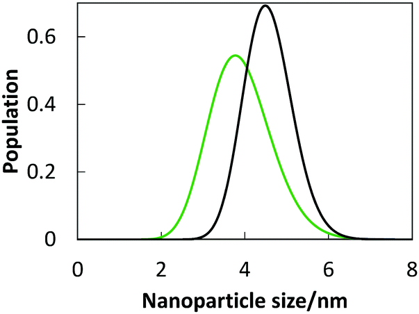 | ||
| Fig. 6 Particle size distribution of samples 7 (green) and 8 (black), as measured by SAXS. | ||
In summary, controlling the atmosphere of the sputtering chamber via monitoring the cathode voltage and plasma colour allows the control of the degree of oxidation for the obtained TiOx NPs dispersed in PEEL. In all samples, uniform and well dispersed TiOx NPs of less than 5 nm were achieved. The main product under blue-plasma sputtering conditions was TiO2 (some oxygen deficient TiO2 particles were also obtained), which does not affect the transparency of the NP-containing PEEL, while the green-plasma sputtering conditions yielded primarily TiO particles, which cause the NP dispersions to become coloured with high visible absorption.
Refractive index increment, colour and transparency of TiOx NPs embedded in resins
As shown above, the sizes of the dispersed TiOx NPs are one or two orders of magnitude smaller than the wavelengths of light in the visible region. This allows the material to have negligible visible light scattering (eqn (SE1), ESI†),35–38 and the preparation of highly transparent resins from PEEL containing TiOx NPs can be achieved. Fig. 7a shows a series of resins exhibiting a high transparency; these resins are made from samples prepared in blue and green plasma. Moreover, owing to non-visible-light-absorption of TiO2 NPs and their small sizes, the colourlessness and transparency of the resin made from sample 1 (60 min blue-plasma sputtering, Fig. 7c) is comparable with that of the resin made from pure PEEL (Fig. 7b). | ||
| Fig. 7 (a) Photograph of the resins, with green sputtering time decreasing from left (120 minutes) to right (0 min), and pictures of resins made from (b) pure PEEL and from (c) sample 1. | ||
Because the addition of high refractive index particles, e.g. TiO2, into low refractive index polymers can improve the refractive index of the composite (eqn (SE2), ESI†), we investigate the refractive index of various resins made using titanium oxide NPs dispersed in PEEL. The results (Fig. 8) show the effect of titanium oxide NPs on the refractive index of the resin. Each dot represents the difference between the refractive indices of a NP-embedded urethane resin sample and of the pure resin. A positive value indicates an increase of the refractive index. The resin made from pure PEEL has a refractive index of 1.5586 ± 0.0005, which increased to 1.5708 ± 0.0005 after 60 min of blue-plasma sputtering under optimal conditions (sample 1), corresponding to an increase in the refractive index of 0.0122 ± 0.0005. Small increases on this scale were observed in all samples in relation to blue-plasma sputtering time. The increase in the refractive index is, at a constant sputtering rate, proportional to the blue-plasma sputtering time, while inversely proportional to the green-plasma sputtering time. Furthermore, this increment-to-TiO2 ratio was in agreement with previously published results pertaining to other hybrid materials containing titanium dioxide.9,27
 | ||
| Fig. 8 Refractive index changes of each sample after sputtering along with the effect of blue and green-plasma sputtering time. Each symbol corresponds to a set of experiments with blue-plasma sputtering time of 0, 30, and 60 min, in which the green-plasma sputtering time has been varied. | ||
As an extreme case, a sample that underwent only green-plasma sputtering (120 min, sample 4) showed a negative change in the refractive index compared to that of the pure resin. The results for mixed sputtering modes show how the blue and green-plasma sputtering compete against each other in terms of increasing the refractive index of the composite materials. In particular, the refractive index measurements clearly demonstrate the importance of the TiO2 formation process, as only blue-plasma sputtering can produce high index NPs. This demonstrates that the conditions for increasing the refractive index of low vapour pressure compounds involve TiO2 formation during blue-plasma sputtering.
Under blue-plasma sputtering conditions, the NPs are formed by etching the TiO2 thin film that continuously regenerates on the titanium plate surface. On the other hand, when there is little oxygen in the atmosphere, atomic clusters of titanium and some titanium monoxide NPs get detached, which are subsequently oxidized to form a uniform TiO film. For each sample the Abbe number was above 40; this value corresponds to materials with low light dispersion characteristics (eqn (SE3), ESI†), making the samples suitable for optical applications.
As the degree of interaction between the PEEL and the NPs is low, this technique can theoretically be applied to any low vapour pressure monomer and obtain similar results. The dispersion of NPs in PEEL is enough stable (for several days) before polymerization to form resins (Fig. S5, ESI†). The effect of the kind of monomers on the dispersion and stability of NPs can be considered more in depth in future studies. The amount of titanium oxide inserted into the matrix was calculated to be approximately 1.4 vol% of the nanocomposite. Considering the low loading amount of titanium oxide NPs, the photodegradation of organic moieties is seemingly negligible.27
The low sputtering rate of our device affected the amount of titanium that could be sputtered, therefore, this limited the refractive index increase. By using higher sputtering rate devices this deficiency can be overcome, allowing the production of transparent resins featuring higher concentrations of TiO2 NPs.
Conclusions
Our new molten matrix sputtering (MMS) was applied to a Ti target for the first time, synthesizing titanium oxide NPs of less than 5 nm embedded in pentaerythritol ethoxylate (3/4 EO/OH). TiO2 or TiO particles could be formed by controlling the atmosphere in the sputtering chamber. The optical properties of the obtained nanocomposite compound containing titanium oxide nanoparticles were varied systematically by changing the atmosphere of the sputtering chamber. Urethane resins incorporating titanium oxide NPs were obtained and the formation of TiO2 positively contributed to increasing the refractive index of the NP-embedded resin. The limiting factor upon increasing the refractive index of the nanocomposite material was the sputtering rate, which was limited by overheating of the titanium sputtering target. In the samples prepared in this study, nanoparticle agglomeration was not observed and the samples were stable over time. This preparation method is advantageous in allowing for the control of nanoparticle oxidation, optical properties, and achieving enhanced refractive indices in these kinds of nanoparticle–monomer systems.Acknowledgements
This work was partially supported by Hokkaido University (to MTN, TY and YI). MTN thanks the E3 program of Hokkaido University. This work was partially supported by Grant-in-Aid for Scientific Research (A) (to TY 24241041) from JSPS, Japan and Grant-in-Aid for Scientific Research in Priority Area (to TY 25102501) from MEXT, Japan and Murata Foundation. MP thanks for the financial support from the Japanese government for his stay in Sapporo. SAXS measurements have been performed under the approval of the Photon Factory Program Advisory Committee (Proposal No. 2014G538). Authors would like to thank Prof. K. Hino (Aichi University of Education) for the measurements of SAXS.References
- A. N. Shipway, E. Katz and I. Willner, ChemPhysChem, 2000, 1, 18–52 CrossRef CAS PubMed.
- R. Cui, C. Liu, J. Shen, D. Gao, J.-J. Zhu and H.-Y. Chen, Adv. Funct. Mater., 2008, 18, 2197–2204 CrossRef CAS.
- M. Wilhelm, M. Adam, M. Bäumer and G. Grathwhol, Adv. Eng. Mater., 2008, 10, 241–245 CrossRef CAS.
- C. Lu and B. Yang, J. Mater. Chem., 2009, 19, 2884–2901 RSC.
- A. A. Ayi, V. Khare, P. Strauch, J. Girard, K. M. Fromm and A. Taubert, Monatsh. Chem., 2010, 141, 1273–1278 CrossRef CAS.
- M. Niederberger, Acc. Chem. Res., 2007, 40, 793–800 CrossRef CAS PubMed.
- L. L. Beecroft and C. K. Ober, Chem. Mater., 1997, 9, 1302–1317 CrossRef CAS.
- W. Caseri, Macromol. Rapid Commun., 2000, 21, 705–722 CrossRef CAS.
- R. J. Nussbaumer, W. R. Caseri, P. Smith and T. Tervoort, Macromol. Mater. Eng., 2003, 288, 44–49 CrossRef CAS.
- G. Garnweitner and M. Niederberger, J. Mater. Chem., 2008, 18, 1171–1182 RSC.
- M. Grätzel, Inorg. Chem., 2005, 44, 6841–6851 CrossRef PubMed.
- A. Choukourov, P. Solar, O. Polonskyi, J. Hanus, M. Drabik, O. Kylian, E. Pavlova, D. Slavinska and H. Biederman, Plasma Processes Polym., 2010, 7, 25–32 CrossRef CAS.
- H. Wender, L. F. de Oliveira, P. Migowski, A. F. Feil, E. Lissner, M. H. G. Prechtl, S. R. Teixeira and J. Dupont, J. Phys. Chem. C, 2010, 114, 11764–11768 CAS.
- T. Torimoto, K. Okazaki, T. Kiyama, K. Hirahara, N. Tanaka and S. Kuwabata, Appl. Phys. Lett., 2006, 89, 243117 CrossRef.
- S. Suzuki, T. Suzuki, Y. Tomita, M. Hirano, K. Okazaki, S. Kuwabata and T. Torimoto, CrystEngComm, 2012, 14, 4922–4926 RSC.
- M. T. Nguyen, T. Yonezawa, Y. Wang and T. Tokunaga, Mater. Lett., 2016, 171, 75–78 CrossRef CAS.
- I. Akita, Y. Ishida and T. Yonezawa, Bull. Chem. Soc. Jpn., 2016, 89, 1054–1056 CrossRef.
- Y. Shishino, T. Yonezawa, K. Kawai and H. Nishihara, Chem. Commun., 2010, 46, 7211–7213 RSC.
- Y. Shishino, T. Yonezawa, S. Udagawa, K. Hase and H. Nishihara, Angew. Chem., Int. Ed., 2011, 50, 703–705 CrossRef CAS PubMed.
- Y. Ishida, S. Udagawa and T. Yonezawa, Colloids Surf., A, 2016, 498, 106–111 CrossRef CAS.
- Y. Ishida, S. Udagawa and T. Yonezawa, Colloids Surf., A, 2016, 504, 437–441 CrossRef CAS.
- Y. Ishida, R. Nakabayashi, M. Matsubara and T. Yonezawa, New J. Chem., 2015, 39, 4227–4230 RSC.
- T. Sumi, S. Motono, Y. Ishida, N. Shirahata and T. Yonezawa, Langmuir, 2015, 31, 4323–4329 CrossRef CAS PubMed.
- Y. Ishida, C. Lee and T. Yonezawa, Sci. Rep., 2015, 5, 15372 CrossRef CAS PubMed.
- Y. Ishida, T. Sumi and T. Yonezawa, New J. Chem., 2015, 39, 5895–5897 RSC.
- Y. Ishida, I. Akita, T. Sumi, M. Matsubara and T. Yonezawa, Sci. Rep., 2016, 6, 29928 CrossRef PubMed.
- C.-C. Chang, L.-P. Cheng, C.-Y. Lin and Y.-Y. Yu, J. Sol–Gel Sci. Technol., 2012, 63, 30–35 CrossRef CAS.
- P. Simon, B. Pignon, B. Miao, S. Coste-Laconte, Y. Laconte, S. Marguet, P. Jegou, B. Bouchet-Fabre, C. Reynaud and N. Herlin-Boime, Chem. Mater., 2010, 23, 3704–3711 CrossRef.
- T. Matsuda, Y. Funae, M. Yoshida, T. Yamamoto and T. Takaya, J. Appl. Polym. Sci., 2000, 76, 50–54 CrossRef CAS.
- L. Dreesen, F. Cecchet and F. S. Lucas, Plasma Processes Polym., 2009, 6, S849–S854 CrossRef CAS.
- Y. Wang, L. Li, K. Yang, L. A. Samuelson and J. Kumar, J. Am. Chem. Soc., 2007, 129, 7238–7239 CrossRef CAS PubMed.
- C. Xue, T. Yonezawa, M. T. Nguyen and X. Lu, Langmuir, 2015, 31, 1575–1580 CrossRef CAS PubMed.
- S. Srivastava, J. P. Thomas, M. A. Rahman, M. Abd-Ellah, M. Mohapatra, D. Pradhan, N. F. Heinig and K. T. Leung, ACS Nano, 2014, 8, 11891–11898 CrossRef CAS PubMed.
- K. Madhusudan, S. V. Manorama and A. Ramachandra, Mater. Chem. Phys., 2002, 78, 239–245 CrossRef.
- E. C. Hao, G. C. Schatz, R. C. Johnson and J. T. Hupp, J. Chem. Phys., 2002, 117, 5963–5966 CrossRef CAS.
- L. F. Donaghey and K. G. Geraghty, Thin Solid Films, 1976, 38, 271–280 CrossRef CAS.
- Y.-Q. Li, S.-Y. Fu, Y. Yang and Y.-W. Mai, Chem. Mater., 2008, 20, 2637–2643 CrossRef CAS.
- B. S. Luk'yanchuk, M. I. Tribel'skii and V. V. Ternovskii, J. Opt. Technol., 2005, 73, 371–377 CrossRef.
Footnotes |
| † Electronic supplementary information (ESI) available: Schematic illustration of the magnetron sputtering device; XRD patterns of the glass substrate and blue-plasma sputtered thin films before and after annealing, UV-Vis spectra of PEEL and the 30 minute blue-plasma sputtered samples; the TEM image of a sample sputtered under blue-plasma conditions; UV-Vis spectra for the as-synthesized blue-plasma sputtered sample and for the same sample after 3 days. Equations for the approximation of the refractive index of composite compounds, scattering probability of a photon passing through a nanoparticle, and the Abbe number. See DOI: 10.1039/c6nj01624c |
| ‡ Present address: Graduate School of Science and Technology, Gunma University, Tenjin-cho, Kiryu, Gunma 376-8516, Japan. |
| This journal is © The Royal Society of Chemistry and the Centre National de la Recherche Scientifique 2016 |