Shape-dependent optoelectrical investigation of Cu2+xCd1−xSnS4 thin films for solar cell applications†
Abstract
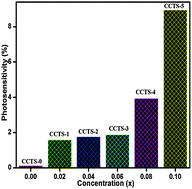
Cu2+xCd1−xSnS4 thin films were prepared with excess Cu concentrations (x = 0, 0.02, 0.04, 0.06, 0.08 and 0.1) by a successive ionic layer adsorption and reaction (SILAR) method. The deposited films were characterized by X-ray diffraction (XRD), field emission scanning electron microscopy (FESEM), transmission electron microscopy (TEM), UV-visible spectroscopy and I–V analysis. XRD analysis confirms the formation of tetragonal structured Cu2CdSnS4 thin films for all the excess Cu concentrations, while the corresponding FESEM images showed microstructural change. It may be attributed to the injection of excess Cu atoms into the Cd sites of the Cu2CdSnS4. The absorption coefficient is found to be greater than 104 cm−1 in the visible region and the bandgap energy is slightly tuned from 1.68 eV to 1.58 eV when compared to Cu2CdSnS4. The Cu2.1Cd0.9SnS4 film showed the highest photoresponse.
 Please wait while we load your content...

