
Type-I van der Waals heterostructure formed by MoS2 and ReS2 monolayers†
Matthew Z.
Bellus
a,
Ming
Li
bc,
Samuel D.
Lane
a,
Frank
Ceballos
a,
Qiannan
Cui
a,
Xiao Cheng
Zeng
*b and
Hui
Zhao
 *a
*a
aDepartment of Physics and Astronomy, The University of Kansas, Lawrence, Kansas 66045, USA. E-mail: huizhao@ku.edu
bDepartment of Chemistry and Department of Mechanical and Materials Engineering, University of Nebraska-Lincoln, Lincoln, NE 68588, USA. E-mail: xzeng1@unl.edu
cCollege of Chemical Engineering, North China University of Science and Technology, Tang Shan, Hebei 063000, China
First published on 23rd September 2016
Abstract
We report a van der Waals heterostructure formed by monolayers of MoS2 and ReS2 with a type-I band alignment. First-principle calculations show that in this heterostructure, both the conduction band minimum and the valence band maximum are located in the ReS2 layer. This configuration is different from previously accomplished type-II van der Waals heterostructures where electrons and holes reside in different layers. The type-I nature of this heterostructure is evident by photocarrier dynamics observed by transient absorption measurements. We found that carriers injected in MoS2 transfer to ReS2 in about 1 ps, while no charge transfer was observed when carriers are injected in ReS2. The carrier lifetime in the heterostructure is similar to that in monolayer ReS2, further confirming the lack of charge separation. We attribute the slower transfer time to the incoherent nature of the charge transfer due to the different crystal structures of the two materials forming the heterostructure. The demonstrated type-I semiconducting van der Waals heterostructure provides new ways to utilize two-dimensional materials for light emission applications, and a new platform to study light–matter interaction in atomically thin materials with strong confinement of electrons and holes.
Conceptual insightsA type-I van der Waals heterostructure is demonstrated. Existing research on vertical van der Waals heterostructures formed by semiconducting two-dimensional materials have focused on structures showing type-II band alignments, where electrons and holes reside in different atomic layers. In the type-I heterostructure formed here, by stacking monolayers of MoS2 and ReS2, both electrons and holes are confined in ReS2. Traditional semiconducting heterostructures based on ionic and covalent compounds are important artificial materials for electronic and optoelectronic technologies. Type-I band alignment has been widely achieved in such materials, in the form of semiconducting quantum wells. Due to the enhanced light-matter interaction by confining electrons and holes in the same region, these heterostructures are widely used in light emitting diodes and semiconductor lasers. However, the lattice-matching requirement severely limits the selection of partner materials. The van der Waals materials have the potential to unleash this constrain on achieving “on-demand” properties, and therefore transform the research on semiconductor heterostructures. The demonstration of the type-I band alignment diversifies the current research on van der Waals heterostructures, enables design and fabrication of complex band landscapes, and facilitates application of van der Waals heterostructures in light emitting devices. |
1 Introduction
Forming heterostructures by combining two materials is one of the key approaches to control electrons in semiconductors, which has led to discoveries such as integer,1 fractional,2 and quantum spin Hall effects,3,4 as well as exciton-polariton condensations.5 Functional materials based on heterostructures are the cornerstone of many applications including semiconductor lasers and light emitting diodes. Depending on the work functions of the involved materials, two types of band alignments can be formed in heterostructures. A type-I alignment refers to the case where both the conduction band minimum (CBM) and the valence band maximum (VBM) are located in the material with the narrower bandgap, as shown in Fig. 1(a) and (b). Electrons and holes excited in the wide-gap material transfer to the narrow-gap material, as indicated by the arrows. The quantum confinement of electrons and holes in the same region facilitates their radiative recombination, which is desirable in light-emitting applications.6 Carriers excited in the narrow-gap material are prohibited from interlayer transfer due to their lower energies. When the CBM and VBM are located in different materials, the alignment is called type-II. Fig. 1(c) and (d) show the situation where the CBM and VBM are located in the narrow-gap and wide-gap materials, respectively. In this case, excitation of the wide-gap material is followed by the transfer of electrons, but not the holes, while opposite charge transfer occurs when the narrow-gap material is excited. The separation of the electrons and holes to different layers can increase their lifetime, and is desired for applications in photovoltaics and photodetection.7–10 | ||
| Fig. 1 Schematic of the band alignment between two semiconductors, showing type-I (a and b) and type-II (c and d) alignments. | ||
The newly developed two-dimensional materials brought the semiconductor heterostructures to a new regime exhibiting an ultimate thinness, atomically sharp and near-defect-free interfaces, exceptional mechanical flexibility, and chemical stability.11,12 More importantly, van der Waals interlayer coupling imposes almost no restrictions on the selection of component materials, opening up a huge number of combinations to explore and utilize. So far, most semiconducting van der Waals heterostructures are composed of monolayers (MLs) of different materials in the family of transition metal dichalcogenides (TMDs). Using the four most extensively studied TMDs, namely MoS2, MoSe2, WS2, and WSe2, 6 combinations exist, and have all been studied: MoS2–MoSe2,13 MoS2–WS2,14–18 MoS2–WSe2,19–25 MoSe2–WSe2,26 MoSe2–WSe2,27 and WS2–WSe2.28 These heterostructures were all found to be type-II, with qualitatively similar electronic and optical properties. Hence, demonstration of a semiconducting van der Waals heterostructure with type-I band alignment is of fundamental importance for control of electrons in atomically thin materials. Such a structure can facilitate applications of van der Waals heterostructures for light emitting devices and enable designs of sophisticated bandgap landscaping in functional materials. It will also provide a platform to study light–matter interaction in atomically thin systems with adjustable confinement energy, and to study the transport of electron–hole pairs and excitons across van der Waals interfaces. Here we demonstrate the first type-I semiconducting van der Waals heterostructure, MoS2–ReS2.
2 Results and discussion
Our first-principle computation results of the electronic structures of ReS2 and MoS2 MLs, as well as the MoS2–ReS2 heterostructure, are shown in Fig. 2(a) and (b). Details of the first-principle computation are given in the ESI.†Fig. 2(a) shows the computed band alignment for ML MoS2 and ReS2. Clearly, the VBM of ReS2 is higher than that of MoS2, while the CBM of ReS2 is lower than that of MoS2. Hence, the band-alignment information alone already suggests that the MoS2–ReS2 heterostructure is likely to exhibit type I band alignment. Computed band structures of MoS2–ReS2 heterostructure is depicted in Fig. 2(b). It can be seen that the CBM is located at the Γ point while the VBM is located at the point between K and Γ. Nevertheless, both CBM and VBM are contributed in ReS2, consistent with the band alignment computation. Note also that the computed bandgap of ReS2 (1.32 eV) is slightly less than the measured optical gap (1.52 eV, see below) because computation based on generalized gradient approximation (see ESI†) tends to underestimate the bandgap. | ||
| Fig. 2 (a) Schematic of the band alignment between MoS2 and ReS2. (b) Calculated bandstructure for the MoS2–ReS2 heterostructure. (c) Sample image showing the isolated monolayer (ML) regions as well as the heterostructure region. (d) Optical contrast in the green channel along the indicated yellow line in (c). (e) Raman spectra of ReS2 (Green) and MoS2 (Red) flakes. | ||
Fig. 2(c) shows the fabricated heterostructure sample of MoS2/ReS2. The individual MLs were mechanically exfoliated from bulk crystals onto polydimethylsiloxane substrates and sequentially transferred to a Si/SiO2 (90 nm) substrate. The sample was then annealed at 200 °C in an Ar/H2 (100 sccm/5 sccm) environment at a base pressure of about 3 Torr. The thickness of the flakes was confirmed to be ML by optical contrast, photoluminescence, and Raman measurements. Fig. 2(d) shows optical contrast along the yellow line in (c) from the green channel of the image. The contrast of about 12 to 13% for each layer is consistent with previous reports for TMD MLs,29,30 and in particular, ReS2 MLs.31 Photoluminescence of the MoS2 flake is also consistent with its ML thickness (see ESI†). Furthermore, Raman spectra of both the ReS2 (Green) and MoS2 (Red) flakes are shown in Fig. 2(e), providing further evidence of ML thickness.32–36 Specifically, the separation of the E12g and A1g peaks is used to confirm the ML thickness of the MoS2 flake,32 while the separation of the I and III peaks is consistent with previous results of ReS2 MLs33 (see ESI†). The ML flakes were large enough to provide a sufficiently large overlapped region as well as isolated ML regions for a thorough control experiment. The sample was under ambient conditions in all the measurements.
The nature of the band alignment of MoS2–ReS2 was revealed by studying its photocarrier dynamics with transient absorption measurements. First, a pump pulse of 1.67 eV and 300 fs was focused to the ReS2 ML region, with a spot size of about 2.2 μm and a fluence of 7 μJ cm−2. Since the measured optical bandgap of ML ReS2 is about 1.52 eV,37 the pump pulse injects photocarriers in ReS2 by interband absorption. With an absorption coefficient of 8 × 10⁶ m−1 (bulk value38), the peak injected density is about 1.4 × 1011 cm−2. The dynamics of these photocarriers is monitored by measuring the differential reflection of a 1.53 eV probe pulse, tuned slightly above the band gap of ReS2. The differential reflection is defined as ΔR/R0 = (R − R0)/R0, where R and R0 are the reflection of the probe with and without the presence of photocarriers, respectively. This quantity is proportional to the carrier density in all the configurations used in this study (see ESI†). The measured differential reflection signal is shown as the open red squares in Fig. 3. The decay of the signal can be fit by a single-exponential function with a background (black curve). The decay constant of 65 ± 5 ps can be attributed to the recombination lifetime of the photocarriers.
 | ||
| Fig. 3 Differential reflection of a 1.53 eV probe for different pump wavelengths and sample regions: the green and red symbols correspond to the pumps of 1.85 and 1.67 eV, respectively. The open and solid symbols represent measurements on the ReS2 monolayer (ML) and the MoS2–ReS2 heterostructure regions, respectively. | ||
Similar results were obtained when the measurement was performed on the MoS2–ReS2 heterostructure, shown as the solid red squares in Fig. 3. With the energy of the lowest excitonic state at 1.85 eV, the MoS2 layer of the heterostructure was neither pumped nor probed. However, the MoS2 layer could serve as a channel for charge transfer if the band alignment were type-II. Specifically, if the CBM (VBM) were lower (higher) in MoS2 compared to ReS2, electrons (holes) would be expected to transfer to MoS2 [see Fig. 1(c) and (d)]. If either transfer occurred, one would expect a smaller signal magnitude (by about a factor of 2) due to the loss of one type of carrier in ReS2 and a slower decay of the signal due to a longer carrier lifetime, resulting from the spatial separation of the electrons and holes. Hence, this result indicates the lacks of charge transfer and indirect exciton formation in MoS2–ReS2, both of which have been generally observed in type-II TMD heterostructures.13–28
The lack of charge transfer could originate from the type-I band alignment or a poor interface quality. To rule out the latter, we studied charge transfer from MoS2 to ReS2 by tuning the pump photon energy to the A-exciton resonance of MoS2, 1.85 eV. With a peak fluence of 7 μJ cm−2, the pump injects excitons in MoS2 with a peak density of 4.8 × 1011 cm−2 (according to an absorption coefficient of 3 × 10⁷ m−1).39 For type-I alignment, these excitons should transfer to ReS2, resulting in an increase of the signal from the 1.67 eV pump. The signal (solid green squares) is indeed increased, by about a factor of 3, and decays with a similar time constant (62 ps, blue curve) as the ReS2 ML. Both features suggest that excitons injected in MoS2 transfer to ReS2, confirming the high quality of the interface. To confirm that the increased signal is not from additional carriers injected in ReS2, due to the larger pump photon energy, we repeated the measurement on the ReS2 ML, shown as the open green squares. The signal is similar to that obtained with the 1.67 eV pump (open red squares), confirming that the signal from ReS2 alone is rather insensitive to the pump photon energy in this range. This is also consistent with previous observations that the absorption coefficient of ReS2 does not change significantly in the range of 1.67–1.85 eV.40
Further evidence of the type-I band alignment was obtained by probing the MoS2 layer, as summarized in Fig. 4. At first, a 3.06 eV pump pulse was used to inject photocarriers in the MoS2 ML region. From the fluence of 12 μJ cm−2, a peak injection density of 3.4 × 1012 cm−2 is estimated, using an absorption coefficient of 1.5 × 10⁸ m−1.39 Shown as the solid squares in Fig. 4, a differential reflection signal on the order of 10−3 was observed with a 1.85 eV probe, tuned to the A-exciton of ML MoS2. Next, we used a 1.53 eV pump with a fluence of 33 μJ cm−2 to inject photocarriers in the ReS2 layer of the heterostructure with a peak carrier density of 7.6 × 1011 cm−2. If the band alignment were type-II, either electrons or holes would transfer to MoS2 [Fig. 1(c) and (d)]. With such a density, the transferred carriers are expected to induce a differential reflection signal of the 1.85 eV probe on the order of 10−4. However, as shown by the open squares in Fig. 4, no signal above 10−4 was observed. This further confirmed the lack of charge transfer from ReS2 to MoS2 in the heterostructure.
 | ||
| Fig. 4 Differential reflection of a 1.85 eV probe from MoS2 monolayer (ML) with a 3.06 eV pump (solid squares) and MoS2–ReS2 heterostructure with a pump of 1.53 eV (open squares). | ||
The demonstrated type-I band alignment of MoS2–ReS2 allows us to study the interlayer transfer process of photocarriers in this configuration, as summarized in Fig. 5. In this figure, all the differential reflection signals are normalized in order to facilitate a visual comparison. First, a 1.85 eV pulse with a peak fluence of 7 μJ cm−2 was used to pump the heterostructure. According to the absorption coefficients of the two MLs, the peak densities of photocarriers injected in the MoS2 and ReS2 layers are 4.8 × 1011 cm−2 and 1.3 × 1011 cm−2, respectively. By probing the ReS2 layer with a 1.53 eV pulse, we monitored the evolution of photocarrier population in that layer, and hence time resolved the transfer of photocarriers from the MoS2 layer to the ReS2 layer. We found a rather slow rise of the signal, as shown by the solid green squares. The contribution of the photocarriers directly injected in ReS2 can be isolated by the control experiment on ML ReS2, under the same conditions, as shown by the open green squares. The actual magnitude of this signal is about one third of the signal from the heterostructure, which is consistent with the ratio of the carriers injected in the two layers. Clearly, the rising of the signal is much faster in ML ReS2, confirming that the slower rising observed in the heterostructure originates from the transfer of photocarriers across the interface. We found that the rising part of the signal can be fit by N1[1 − exp(−t/τT)] + N2, where N1 and N2 represent the photocarrier densities injected in MoS2 and ReS2 layers, respectively, and τT the transfer time. As shown by the solid green curve in Fig. 5, this expression can satisfactorily describe the data, with a transfer time of 1.3 ± 0.1 ps.
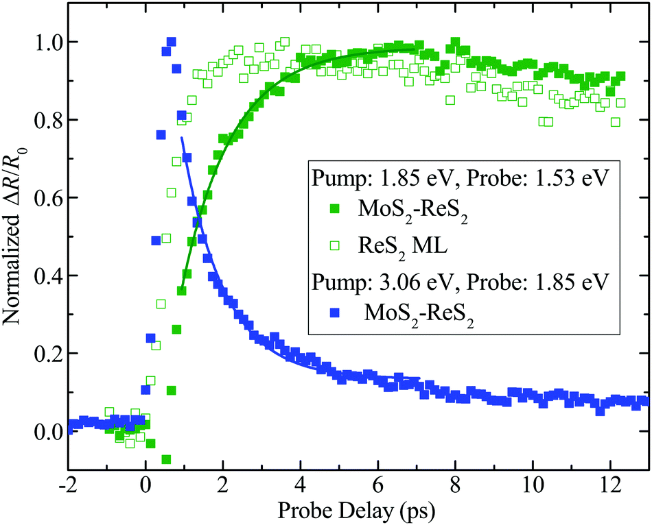 | ||
| Fig. 5 Differential reflection signal of the 1.53 eV probe with 1.85 eV pump measured from MoS2–ReS2 (solid green squares) and monolayer (ML) ReS2 (open green squares). The solid blue squares are measured from MoS2–ReS2 heterostructure with a pump of 3.06 eV and probe of 1.85 eV. The solid curves are fits to the data. | ||
In addition to time resolving the photocarrier build-up process in ReS2, an alternative way to study the photocarrier transfer is to monitor the decay of population in MoS2. For that purpose, we used a 3.06 eV pump pulse to inject photocarriers in the heterostructure and a probe pulse of 1.85 eV to monitor the population of carriers in MoS2. Carriers injected in ReS2 are not sensed by this probe. The results are shown as the blue squares in Fig. 5. The signal decays single-exponentially with a time constant of 1.1 ± 0.2 ps, as indicated by the blue curve. Such a decay is significantly faster than that obtained from the MoS2 ML (black squares in Fig. 4), which reflects the exciton recombination time. This fast decay is due to the transfer of photocarriers to ReS2, and the time constant matches τT, obtained by monitoring the build-up of population in ReS2, very well.
Recent studies have revealed that charge transfer in type-II heterostructures formed by TMDs occurs on an ultrafast time scale, shorter than 100 fs,13,14,27 which can be facilitated by quantum coherence.41 The transfer process observed here is different from the previous studies in two aspects. First, in type-II heterostructures, electrons and holes transfer to opposite layers, and the Coulomb field is along the opposite direction of charge transfer. Here, the transfer is ambipolar, with both types of carriers moving together. Second, the previously studied heterostructures were formed by TMDs with the same 2H crystal structure. Here, the heterostructure is formed by 2H-MoS2 and ReS2 with a distorted 1T structure. It is possible that the different lattice structures suppress the coherent transfer process, and result in an incoherent, and thus slower, transfer process.
3 Conclusions
We have shown, both theoretically and experimentally, that MoS2 and ReS2 MLs form a type-I van der Waals heterostructure with both the CBM and VBM located in ReS2. By selectively exciting photocarriers into the different layers of the heterostructure and probing the ReS2 layer, we obtained evidence for carrier transfer from the MoS2 layer to the ReS2 layer. When probing the exciton resonance of MoS2, a fast decay time in the heterostructure relative to ML MoS2 is a further indication that both electrons and holes are transferring to the ReS2. We observed that the transfer time of these carriers occurs on the order of 1 ps, which is significantly slower than the interlayer transport observed in previously studied TMD heterostructures with type-II band alignment. We attribute this to the incoherent nature of the transfer process between the two materials with different lattice structures. Overall, this observation of a type-I TMD heterostructure further proves the versatility of this family of materials to reach a broad range of applications, where band alignment plays a crucial role in charge transfer phenomena. The results also shed light on the fundamental understanding of charge transfer at van der Waals interfaces.Acknowledgements
We thank Qingfeng Liu and Judy Wu for their help on Raman measurements. This material is based upon work supported by the National Science Foundation of USA under Award No. DMR-1505852 and IIA-1430493. XCZ was supported by the National Science Foundation of USA through the Nebraska Materials Research Science and Engineering Center (MRSEC) (grant No. DMR-1420645) and by the Nebraska Center for Energy Sciences Research in University of Nebraska – Lincoln. The computation was carried out at the Holland Computing Center and on NC3 computers in the Department of Chemistry at University of Nebraska – Lincoln.References
- K. von Klitzing, Rev. Mod. Phys., 1986, 58, 519–531 CrossRef CAS.
- D. C. Tsui, H. L. Stormer and A. C. Gossard, Phys. Rev. Lett., 1982, 48, 1559–1562 CrossRef CAS.
- B. A. Bernevig and S. C. Zhang, Phys. Rev. Lett., 2006, 96, 106802 CrossRef PubMed.
- M. König, S. Wiedmann, C. Brüne, A. Roth, H. Buhmann, L. W. Molenkamp, X. L. Qi and S. C. Zhang, Science, 2007, 318, 766–770 CrossRef PubMed.
- J. Kasprzak, M. Richard, S. Kundermann, A. Baas, P. Jeambrun, J. M. J. Keeling, F. M. Marchetti, M. H. Szymanska, R. Andre, J. L. Staehli, V. Savona, P. B. Littlewood, B. Deveaud and L. S. Dang, Nature, 2006, 443, 409–414 CrossRef CAS PubMed.
- Z. H. Lu, D. J. Lockwood and J. M. Baribeau, Nature, 1995, 378, 258–260 CrossRef CAS.
- S. S. Lo, T. Mirkovic, C. H. Chuang, C. Burda and G. D. Scholes, Adv. Mater., 2011, 23, 180–197 CrossRef CAS PubMed.
- P. Peng, D. J. Milliron, S. M. Hughes, J. C. Johnson, A. P. Alivisatos and R. J. Saykally, Nano Lett., 2005, 5, 1809–1813 CrossRef CAS PubMed.
- Z. Wang, H. Yin, C. Jiang, M. Safdar and J. He, Appl. Phys. Lett., 2012, 101, 253109 CrossRef.
- F. Wang, Z. X. Wang, K. Xu, F. M. Wang, Q. S. Wang, Y. Huang, L. Yin and J. He, Nano Lett., 2015, 15, 7558–7566 CrossRef CAS PubMed.
- A. K. Geim and I. V. Grigorieva, Nature, 2013, 499, 419–425 CrossRef CAS PubMed.
- K. S. Novoselov, A. Mishchenko, A. Carvalho and A. H. Castro Neto, Science, 2016, 353, 461 CrossRef CAS PubMed.
- F. Ceballos, M. Z. Bellus, H. Y. Chiu and H. Zhao, ACS Nano, 2014, 8, 12717–12724 CrossRef CAS PubMed.
- X. Hong, J. Kim, S. F. Shi, Y. Zhang, C. Jin, Y. Sun, S. Tongay, J. Wu, Y. Zhang and F. Wang, Nat. Nanotechnol., 2014, 9, 682–686 CrossRef CAS PubMed.
- Y. Gong, J. Lin, X. Wang, G. Shi, S. Lei, Z. Lin, X. Zou, G. Ye, R. Vajtai, B. I. Yakobson, H. Terrones, M. Terrones, B. K. Tay, J. Lou, S. T. Pantelides, Z. Liu, W. Zhou and P. M. Ajayan, Nat. Mater., 2014, 13, 1135–1142 CrossRef CAS PubMed.
- Y. F. Yu, S. Hu, L. Q. Su, L. J. Huang, Y. Liu, Z. H. Jin, A. A. Purezky, D. B. Geohegan, K. W. Kim, Y. Zhang and L. Y. Cao, Nano Lett., 2015, 15, 486–491 CrossRef CAS PubMed.
- S. Tongay, W. Fan, J. Kang, J. Park, U. Koldemir, J. Suh, D. S. Narang, K. Liu, J. Ji, J. Li, R. Sinclair and J. Wu, Nano Lett., 2014, 14, 3185–3190 CrossRef CAS PubMed.
- J. T. Yuan, S. Najmaei, Z. H. Zhang, J. Zhang, S. D. Lei, P. M. Ajayan, B. I. Yakobson and J. Lou, ACS Nano, 2015, 9, 555–563 CrossRef CAS PubMed.
- H. Fang, C. Battaglia, C. Carraro, S. Nemsak, B. Ozdol, J. S. Kang, H. A. Bechtel, S. B. Desai, F. Kronast, A. A. Unal, G. Conti, C. Conlon, G. K. Palsson, M. C. Martin, A. M. Minor, C. S. Fadley, E. Yablonovitch, R. Maboudian and A. Javey, Proc. Natl. Acad. Sci. U. S. A., 2014, 111, 6198–6202 CrossRef CAS PubMed.
- M. H. Chiu, M. Y. Li, W. Zhang, W. T. Hsu, W. H. Chang, M. Terrones, H. Terrones and L. J. Li, ACS Nano, 2014, 8, 9649–9656 CrossRef CAS PubMed.
- T. Roy, M. Tosun, X. Cao, H. Fang, D. H. Lien, P. D. Zhao, Y. Z. Chen, Y. L. Chueh, J. Guo and A. Javey, ACS Nano, 2015, 9, 2071–2079 CrossRef CAS PubMed.
- T. Roy, M. Tosun, J. S. Kang, A. B. Sachid, S. B. Desai, M. Hettick, C. C. Hu and A. Javey, ACS Nano, 2014, 8, 6259–6264 CrossRef CAS PubMed.
- R. Cheng, D. Li, H. Zhou, C. Wang, A. Yin, S. Jiang, Y. Liu, Y. Chen, Y. Huang and X. Duan, Nano Lett., 2014, 14, 5590–5597 CrossRef CAS PubMed.
- M. M. Furchi, A. Pospischil, F. Libisch, J. Burgdorfer and T. Mueller, Nano Lett., 2014, 14, 4785–4791 CrossRef CAS PubMed.
- C. H. Lee, G. H. Lee, A. M. van der Zande, W. Chen, Y. Li, M. Han, X. Cui, G. Arefe, C. Nuckolls, T. F. Heinz, J. Guo, J. Hone and P. Kim, Nat. Nanotechnol., 2014, 9, 676–681 CrossRef CAS PubMed.
- P. Rivera, J. R. Schaibley, A. M. Jones, J. S. Ross, S. Wu, G. Aivazian, P. Klement, K. Seyler, G. Clark, N. J. Ghimire, J. Yan, D. G. Mandrus, W. Yao and X. Xu, Nat. Commun., 2015, 6, 6242 CrossRef CAS PubMed.
- F. Ceballos, M. Z. Bellus, H. Y. Chiu and H. Zhao, Nanoscale, 2015, 7, 17523–17528 RSC.
- W. T. Hsu, Z. A. Zhao, L. J. Li, C. H. Chen, M. H. Chiu, P. S. Chang, Y. C. Chou and W. H. Chang, ACS Nano, 2014, 8, 2951–2958 CrossRef CAS PubMed.
- A. Castellanos-Gomez, N. Agraït and G. Rubio-Bollinger, Appl. Phys. Lett., 2010, 96, 213116 CrossRef.
- M. M. Benameur, B. Radisavljevic, J. S. Héron, S. Sahoo, H. Berger and A. Kis, Nanotechnology, 2011, 22, 125706 CrossRef CAS PubMed.
- O. B. Aslan, D. A. Chenet, A. M. van der Zande, J. C. Hone and T. F. Heinz, ACS Photonics, 2016, 3, 96–101 CrossRef CAS.
- H. Li, Q. Zhang, C. C. R. Yap, B. K. Tay, T. H. T. Edwin, A. Olivier and D. Baillargeat, Adv. Funct. Mater., 2012, 22, 1385–1390 CrossRef CAS.
- D. A. Chenet, O. B. Aslan, P. Y. Huang, C. Fan, A. M. van der Zande, T. F. Heinz and J. C. Hone, Nano Lett., 2015, 15, 5667–5672 CrossRef CAS PubMed.
- R. He, J. A. Yan, Z. Y. Yin, Z. P. Ye, G. H. Ye, J. Cheng, J. Li and C. H. Lui, Nano Lett., 2016, 16, 1404–1409 CrossRef CAS PubMed.
- E. Lorchat, G. Froehlicher and S. Berciaud, ACS Nano, 2016, 10, 2752–2760 CrossRef CAS PubMed.
- S. Tongay, H. Sahin, C. Ko, A. Luce, W. Fan, K. Liu, J. Zhou, Y.-S. Huang, C.-H. Ho, J. Yan, D. F. Ogletree, S. Aloni, J. Ji, S. Li, J. Li, F. M. Peeters and J. Wu, Nat. Commun., 2014, 5, 3252 Search PubMed.
- K. Dileep, R. Sahu, S. Sarkar, S. C. Peter and R. Datta, J. Appl. Phys., 2016, 119, 114309 CrossRef.
- K. Friemelt, L. Kulikova, L. Kulyuk, A. Siminel, E. Arushanov, C. Kloc and E. Bucher, J. Appl. Phys., 1996, 79, 9268–9272 CrossRef CAS.
- H.-L. Liu, C.-C. Shen, S.-H. Su, C.-L. Hsu, M.-Y. Li and L.-J. Li, Appl. Phys. Lett., 2014, 105, 201905 CrossRef.
- Q. Cui, J. He, M. Z. Bellus, M. Mirzokarimov, T. Hofmann, H.-Y. Chiu, M. Antonik, D. He, Y. Wang and H. Zhao, Small, 2015, 11, 5565–5571 CrossRef CAS PubMed.
- R. Long and O. V. Prezhdo, Nano Lett., 2016, 16, 1996–2003 CrossRef CAS PubMed.
Footnote |
| † Electronic supplementary information (ESI) available: Characterization of sample thickness, additional data on power dependence of the measurements; computational method. See DOI: 10.1039/c6nh00144k |
| This journal is © The Royal Society of Chemistry 2017 |