
High-speed, solution-coatable memory based on Cu–SiO2 core–shell nanowires†
Patrick F.
Flowers
,
Matthew J.
Catenacci
and
Benjamin J.
Wiley
*
Department of Chemistry, Duke University, Durham, North Carolina 27708, USA. E-mail: benjamin.wiley@duke.edu
First published on 9th May 2016
Abstract
Printable electronics has the potential to drastically reduce the environmental and economic costs associated with the production of electronic devices, as well as enable rapid prototyping of circuits and their printing on demand, similar to what 3D printing has done for structural objects. A major barrier to the realization of printable computers that can run programs is the lack of a solution-coatable non-volatile memory with performance metrics comparable to silicon-based devices. Here we demonstrate a non-volatile memory based on Cu–SiO2 core–shell nanowires that can be printed from solution and exhibits on-off ratios of 106, switching speeds of 50 ns, a low operating voltage of 2 V, and operates for at least 104 cycles without failure. Each of these metrics is similar to or better than Flash memory (the write speed is 20 times faster than Flash). Memory architectures based on the individual memory cells demonstrated here could enable the printing of the more complex, embedded computing devices that are expected to make up an internet of things.
Conceptual insightsThis article reports the first printable memory that exhibits performance characteristics comparable to Flash memory. Based on a network of copper nanowires coated with silica, this memory achieves a 10-fold increase in the number of read/write cycles, as well as a 1000-fold increase in speed and retention time than the next best reported solution-coatable non-volatile memory. Memory architectures based on the individual memory cells demonstrated here could enable the printing of the more complex, embedded computing devices that are expected to make up an internet of things. |
Introduction
A common way to store information in a material is in the form of trapped charge, and this is how information is stored in Flash memory. Printable materials used for charge-based information storage include graphene oxide,1 polymers,2 and nanoparticle–polymer composites.3,4 The fastest write speeds for these materials is on the order of tens of milliseconds (10![[thin space (1/6-em)]](https://www.rsc.org/images/entities/char_2009.gif) 000 times slower than Flash), with up to ∼103 cycles demonstrated for some examples (versus 104–105 cycles for Flash), and retention times of <3 days (versus >10 years for Flash). Ferroelectric polymers have also been used to store information in printed memories that achieved switching speeds as low as 10 ms,5 with degradation in the performance occurring after 103 cycles,6 and only 1 hour of data retention.7 Write speeds as low as 100 µs have been achieved in a phase-change memory based on solution-processed GeTe nanoparticles, but degradation in performance was observed after only 102 cycles, and data retention times were not reported.8 Thus, every solution-coatable alternative to Flash is at best 100 times slower, retains data for periods that are at least 1000 times shorter, and/or fails after 10 times fewer cycles.
000 times slower than Flash), with up to ∼103 cycles demonstrated for some examples (versus 104–105 cycles for Flash), and retention times of <3 days (versus >10 years for Flash). Ferroelectric polymers have also been used to store information in printed memories that achieved switching speeds as low as 10 ms,5 with degradation in the performance occurring after 103 cycles,6 and only 1 hour of data retention.7 Write speeds as low as 100 µs have been achieved in a phase-change memory based on solution-processed GeTe nanoparticles, but degradation in performance was observed after only 102 cycles, and data retention times were not reported.8 Thus, every solution-coatable alternative to Flash is at best 100 times slower, retains data for periods that are at least 1000 times shorter, and/or fails after 10 times fewer cycles.
Resistive switching random access memory (RRAM) is an exciting alternative to Flash in part due to the fact that it can offer write speeds as small as 0.1 ns, 10000 times faster than typical Flash memory.9 RRAM can also offer greater numbers of cycles before failure; up to 1011 switching cycles have been demonstrated.10 Copper-based RRAM devices have demonstrated excellent 10 year data retention at 150 °C.11 These copper-based devices often utilize SiO2 as the solid electrolyte, and resistive switching appears to occur through the formation of a metallic filament.12–14 However, these studies required the use of evaporation techniques to deposit metal-active layer-metal sandwich structures with thin/uniform active layers.
Several authors have reported resistive switching in ∼100 nm-thick films of solution-processed solid electrolyte layers (e.g., TiO2 or ZnO) sandwiched between metal electrodes, but none of these studies have reported switching speeds, and they have demonstrated at most 500 cycles.15 High-performance RRAM devices made with vapor-based methods typically employ a solid electrolyte 3–50 nm-thick, and obtaining a continuous, smooth, solution-processed film with a thickness in this range is challenging.9,10
An alternative approach is to employ nanowires coated with an electrolyte layer with the appropriate thickness.16 This concept was first demonstrated by Dong et al. for crossbars composed of Si/a-Si core–shell nanowires and Ag nanowires.17 This device exhibited writing times of 100 ns, retention times of 2 weeks, and 104 switching cycles. However, this device required the fabrication of metal contacts on individual nanowires with electron beam lithography, and thus is not low-cost or scalable. Cagli et al. have reported magnetically assembling crossbars from Ni–NiO core–shell nanowires, but in this work e-beam lithography was also required to make electrical contact with the nanowires.21 Bellew et al. demonstrated resistive switching in networks of nanowires, which could be contacted by metal evaporation through a shadow mask.22 They proposed that a single nanowire-nanowire junction in the network was responsible for resistive switching. Switching was reported for five cycles, and no switching speed was reported.
Here we report a solution-coatable, non-volatile memory based on resistive switching in single Cu–SiO2 core–shell nanowires that exhibits average on–off ratios of 106, switching speeds of 50 ns, retention times of 4 days, and has been demonstrated to operate for at least 104 cycles without failure. As shown in Table 1, this memory represents a 10-fold increase in number of cycles, and a 1000-fold increase in speed and retention time than the next best reported metric for a solution-coatable non-volatile memory. Fabrication of this nanowire-based memory involves simply coating nanowires from solution onto microfabricated metal electrodes; no e-beam lithography is required. Although we use photolithography to make the electrodes in this paper, they could alternatively be printed from solution using a variety of previously reported methods.23,24
| Technology | Write speed | Write/erase voltages | Data retention time | ON/OFF cycling endurance |
|---|---|---|---|---|
| Comparison of common metrics for evaluating a non-volatile memory are shown here for Flash (the industry standard), the best previously reported performance metrics for printable memory technologies, and this work. Superscript numbers correspond to referenced articles. a The authors here report that the memory was able to function until 105 cycles. However, significant degradation in performance can be seen beginning at 103 cycles. | ||||
| Flash | 1 µs18 | 12 V18 | >10 years18 | 104–105 cycles18,19 |
| Charge trap printable memory | 10 ms2 | 2 V3 | 3 days18,19 | 103 cycles2 |
| Ferroelectric printable memory | 5 ms3 | 15 V20 | 1 hour20 | 103 cycles6a |
| Phase change printable memory | 100 µs8 | 3 V/15 V8 | — | 150 cycles8 |
| Cu@SiO2 NW | 50 ns | 2 V | 4 days | >104 cycles |
Results and discussion
A key advance that enables such high performance in a device that can be made with solution-based processes is the development of a technique to make electrical contact to individual nanowires without the need for electron beam lithography. Fig. 1a shows a scanning electron microscopy (SEM) image of a typical Cu–SiO2 nanowire-based memory cell, which consists of a network of core–shell nanowires deposited across two electrodes. The 15 nm-thick SiO2 shells coating the Cu nanowires (Fig. 1b) serve to electrically insulate all the nanowires from one another and from the electrodes. Electrical contact is made with a single nanowire in the network by applying a positive bias of about 7 V to the copper electrode while the gold electrode is grounded. This bias (1) dissolves the copper electrode to form copper ions, (2) drives the positively charged copper ions across the SiO2 shell, and (3) reduces the ions onto the copper nanowire until a metal filament forms across the gap. Once a conducting filament forms between the copper electrode and the nanowire, filament formation proceeds in a similar manner at the junction between the copper nanowire and the gold electrode until the nanowire is electrically connected to both electrodes. When this occurs, the current rises until a compliance current is reached (Fig. 1c). This process is similar to the initial electroforming step in electrochemical metallization cells.25Fig. 1d and e show a schematic illustration of the initial electroforming process.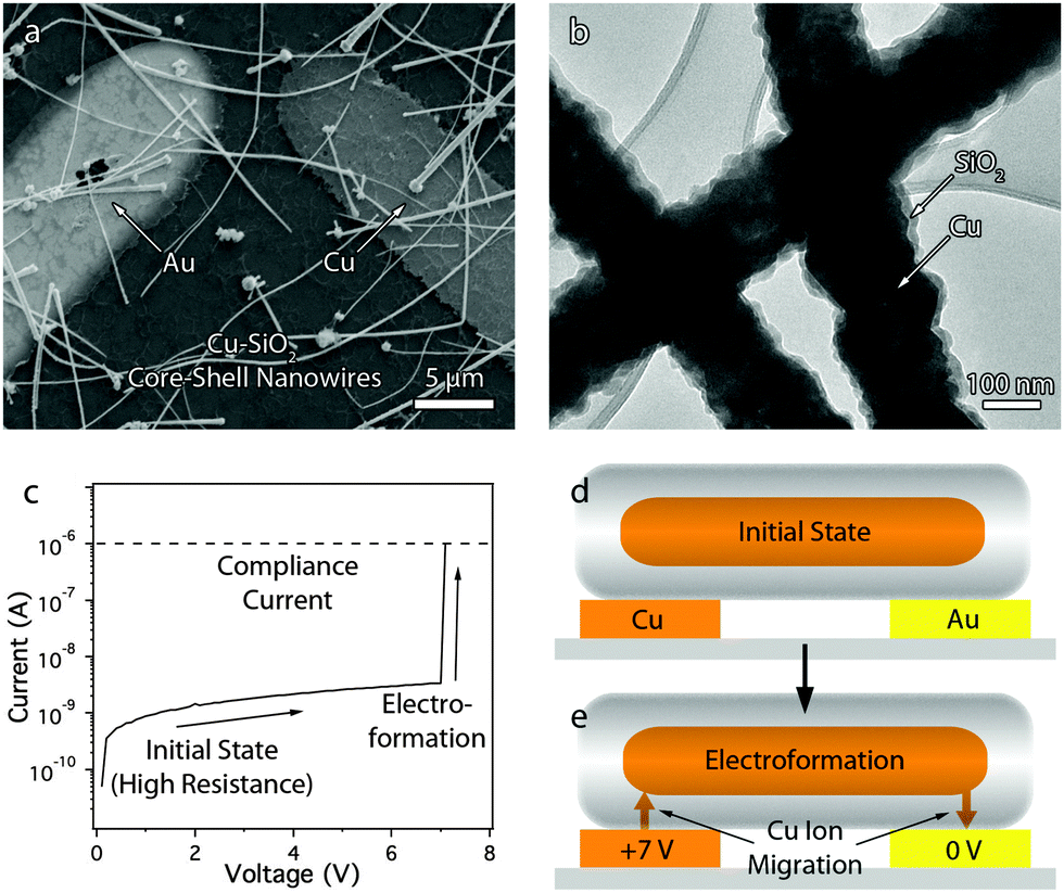 | ||
| Fig. 1 (a) SEM image of memory cell. (b) TEM image of the 15 nm-thick SiO2 shells coating the copper nanowires. (c) A plot of the current and voltage between the electrodes during electroformation. (d) The nanowires are initially electrically isolated from the metal electrodes. (e) Application of +7 V to the Cu electrode drives Cu ions into the SiO2 shell and induces the growth of Cu filaments. | ||
In order to provide further evidence that the memory cell is operating through one nanowire out of a nanowire network between the electrodes, we measured the relationship between electrode size and the ON resistance. If the memory is operating through multiple nanowires, the ON resistance should decrease with increasing electrode size because there are more nanowires available to serve as conducting paths. However, Fig. S1 (ESI†) shows there is no significant effect of electrode size on the resistance of the memory cell in the ON state. This data supports the position the electroforming step selects one nanowire out of the network to serve as the connection between the electrodes.
Once electrical connection of the nanowire to the electrodes is complete, the cell is in the ON (low resistance) state. To reset the memory cell back to the OFF (high resistance) state, a negative bias is applied to the copper electrode, resulting in anodic dissolution of the copper filament between the copper nanowire and the gold electrode (Fig. 2a). The memory cell can be set back to the ON state by subsequent application of a positive bias to the copper electrode. As shown in Fig. 2b, an average of 2.3 V was required to switch the memory ON and −1.2 V was required to switch the memory OFF. This low voltage is compatible with many electronic circuits.26,27 By comparison of the FORM, SET, and RESET traces, the operation of this memory appears very similar to the Cu–SiO2–Pt system described by Schindler et al.13
 | ||
| Fig. 2 (a) The memory can be switched from the ON to OFF state by applying −2 V to the copper electrode so as to dissolve the copper filament. A positive bias can then be applied to switch the memory back to the on state. (b) A plot of the current and voltage between the electrodes during erasing and writing. (c) A plot showing no degradation in performance after 10000 write/erase cycles. | ||
Fig. 2c shows that the device could be switched between the ON and OFF states at least 10000 times, with an average ratio of the resistance in the ON and OFF state (ROFF/RON) of 106. The OFF state resistance appears noisy on the graph because it is at the limit of detection of the instrument. The large difference in resistance between the ON and OFF state ensures that the state of the device can be measured reliably. Fig. S2 (ESI†) shows the cumulative probability of the SET/RESET voltages of a single device over the 10000 cycles. The variability of switching voltages in different devices is shown in Fig. S3 (ESI†).
To measure the retention time of the core–shell nanowire-based memory, four memory cells were switched on and the resistance of each was measured periodically through the application of a 10 mV read pulse (otherwise no bias was applied). The ON state resistance showed negligible degradation after 1 day of exposure to normal atmosphere (Fig. 3). After this point 50% of the devices began to increase in resistance but remained ON (with a resistance below 1 MΩ) for at least 4 days. These results indicate that this technology is moderately resilient to air exposure, but an air-impermeable coating will likely be required to ensure longer-term retention of data.
 | ||
| Fig. 3 A plot of the ON resistance versus time. The ON state resistances of all devices tested were ON for at least 4 days. After this point 50% of the devices tested began to show signs of degradation. | ||
One of the most impressive characteristics of the core–shell nanowire memory is its write speed of 50 ns ± 20 ns (n = 15). This is the fastest write speed of any nanowire-based or solution-coatable memory. An example of one write speed test conducted according to a commonly implemented method for measuring switching speed is shown in Fig. 4a and b.28,29 A low-voltage test pulse was first applied to confirm the cell was in the OFF state. A 15 V write pulse was then applied to switch the cell on, followed by a low-voltage test pulse to confirm the cell was in the on state. Fig. 4b shows an expanded view of the delay between the applied bias and the current response through the memory cell. Fig. S4 (ESI†) provides further information about the testing method and calibration. Three additional devices were also tested (see Fig. S5, ESI†) and all of the devices had comparable write speeds.
 | ||
| Fig. 4 (a) A pulse of voltage was used to turn the memory ON while the current response was measured with an oscilloscope. Lower magnitude voltage pulses were applied before and after the write pulse to verify the state of the memory. (b) Expanded view of the write pulse. The delay (after calibration) between the applied voltage and the current response at 90% of the maximum amplitude was used to determine the write time. | ||
Conclusions
In summary, this letter reports a solution-coatable memory with the highest performance metrics to date. Such performance metrics were achieved in a solution-coatable format by electroforming to single nanowires out of a network of nanowires that span two microfabricated electrodes. In this way, we eliminate the need to fabricate a sub-50 nm electrolyte film to obtain a high-performance resistive switch, and instead use a 15 nm-thick SiO2 shell on the nanowires to serve as the electrolyte. This advance paves the way toward addressable, high-performance memory that can be printed from solution.Author contributions
P. F. F and M. C. designed the experiments and synthesized the nanowires. P. F. F. and B. J. W. designed the experiments and wrote the paper. All authors have given approval to the final version of the manuscript.Acknowledgements
This work was supported in part by Rambus and an NSF CAREER award (Grant DMR-1253534). P. F. F. acknowledges support by a fellowship from the Graduate Certificate Program in Nanoscience at Duke University.References
- C. Kim, J.-M. Song, J.-S. Lee and M. J. Lee, Nanotechnology, 2014, 25, 014016 CrossRef PubMed.
- K. J. Baeg, D. Khim, J. Kim, B. D. Yang, M. Kang, S. W. Jung, I. K. You, D. Y. Kim and Y. Y. Noh, Adv. Funct. Mater., 2012, 22, 2915–2926 CrossRef CAS.
- N. Gogurla, S. P. Mondal, A. K. Sinha, A. K. Katiyar, W. Banerjee, S. C. Kundu and S. K. Ray, Nanotechnology, 2013, 24, 345202 CrossRef PubMed.
- A. Prakash, J. Ouyang and J.-L. LinYang Yang, J. Appl. Phys., 2006, 100, 054309 CrossRef.
- T. N. Ng, D. E. Schwartz, L. L. Lavery, G. L. Whiting, B. Russo, B. Krusor, J. Veres, P. Bröms, L. Herlogsson, N. Alam, O. Hagel, J. Nilsson and C. Karlsson, Sci. Rep., 2012, 2, 585 Search PubMed.
- U. S. Bhansali, M. A. Khan and H. N. Alshareef, Microelectron. Eng., 2013, 105, 68–73 CrossRef CAS.
- J. Y. Bak, S. W. Jung and S. M. Yoon, Org. Electron., 2013, 14, 2148–2157 CrossRef CAS.
- R. Jeyasingh, M. A. Caldwell and D. J. Milliron, ESSDERC, 2011, 99–102 Search PubMed.
- L. Goux, K. Sankaran, G. Kar, N. Jossart, K. Opsomer, R. Degraeve, G. Pourtois, G. M. Rignanese, C. Detavernier, S. Clima, Y. Y. Chen, A. Fantini, B. Govoreanu, D. J. Wouters, M. Jurczak, L. Altimime and J. A. Kittl, VLSIT, 2012, 69–70 Search PubMed.
- M. N. Kozicki, M. Park and M. Mitkova, IEEE Trans. Nanotechnol., 2005, 4, 331–338 CrossRef.
- M. Wang, W. J. Luo, Y. L. Wang, L. M. Yang, W. Zhu, P. Zhou, J. H. Yang, X. G. Gong, Y. Y. Lin, R. Huang, S. Song, Q. T. Zhou, H. M. Wu, J. G. Wu, M. H. Chi, IEEE, 2010, pp. 89–90 Search PubMed.
- Y. Bernard, V. T. Renard and P. Gonon, Microelectron. Eng., 2011, 88, 814–816 CrossRef CAS.
- C. Schindler, G. Staikov and R. Waser, Appl. Phys. Lett., 2009, 94, 072109 CrossRef.
- C. Schindler, M. Weides, M. N. Kozicki and R. Waser, Appl. Phys. Lett., 2008, 92, 122910 CrossRef.
- N. M. Muhammad, N. Duraisamy, K. Rahman, H. W. Dang, J. Jo and K. H. Choi, Curr. Appl. Phys., 2013, 13, 90–96 CrossRef.
- L. He, Z.-M. Liao, H.-C. Wu, X.-X. Tian, D.-S. Xu, G. L. W. Cross, G. S. Duesberg, I. V. Shvets and D.-P. Yu, Nano Lett., 2011, 11, 4601–4606 CrossRef CAS PubMed.
- Y. Dong, G. Yu, M. C. McAlpine, W. Lu and C. M. Lieber, Nano Lett., 2008, 8, 386–391 CrossRef CAS PubMed.
- P. A. Laplante, Real-Time Systems Design & Analysis, John Wiley & Sons, 3rd edn, 2006, p. 42 Search PubMed.
- P. C. Huang, Y. H. Chang and T. W. Kuo, IEEE, 2008, vol. 11, pp. 529–534 Search PubMed.
- H.-T. Lin, Z. Pei, J.-R. Chen, C.-P. Kung, Y.-C. Lin, C.-M. Tseng and Y.-J. Chan, IEEE, 2007, pp. 233–236 Search PubMed.
- C. Cagli, F. Nardi, B. Harteneck, Z. Tan, Y. Zhang and D. Ielmini, Small, 2011, 7, 2899–2905 CrossRef CAS PubMed.
- A. T. Bellew, A. P. Bell, E. K. McCarthy, J. A. Fairfield and J. J. Boland, Nanoscale, 2014, 6, 9632–9639 RSC.
- W.-S. Han, J.-M. Hong, H.-S. Kim and Y.-W. Song, Nanotechnology, 2011, 22, 395705 CrossRef PubMed.
- M. J. Coutts, M. B. Cortie, M. J. Ford and A. M. McDonagh, J. Phys. Chem. C, 2009, 113, 1325–1328 CAS.
- R. Waser, R. Dittmann, G. Staikov and K. Szot, Adv. Mater., 2009, 21, 2632–2663 CrossRef CAS.
- K. J. Baeg, S. W. Jung, D. Khim, J. Kim, D. Y. Kim and J. B. Koo, Org. Electron., 2013, 14, 1407–1418 CrossRef CAS.
- L. Baldi, R. Bez and G. Sandhu, Solid-State Electron., 2014, 102, 2–11 CrossRef CAS.
- I. J. Bahl, Control Components Using Si, GaAs, and GaN Technologies, Artech House, Boston/London, 2014, p. 60 Search PubMed.
- S. W. Lee, S. J. Park, E. E. B. Campbell and Y. W. Park, Nat. Commun., 2011, 2, 220 CrossRef PubMed.
Footnote |
| † Electronic supplementary information (ESI) available: Supplementary methods and supplementary Fig. S1–S3. See DOI: 10.1039/c6nh00020g |
| This journal is © The Royal Society of Chemistry 2016 |