 Open Access Article
Recent progress in fabrication techniques of graphene nanoribbons
Wentao
Xu
and
Tae-Woo
Lee
*
Department of Materials Science and Engineering, Pohang University of Science and Technology (POSTECH), Pohang 790-784, Republic of Korea. E-mail: twlee@postech.ac.kr; taewlees@gmail.com
First published on 11th March 2016
Abstract
Graphene has been the focus of research since its isolation in 2004. However, the lack of a bandgap restricts its application in semiconductor industry in spite of its predicted extremely high carrier mobility (>250![[thin space (1/6-em)]](https://www.rsc.org/images/entities/char_2009.gif) 000 cm2 V−1 s−1). Theoretical studies predict that a band gap will open in quasi-one-dimensional graphene ribbons, due to quantum confinement and edge effects. Consequently, many approaches to prepare GNRs have been developed. However, applications of GNRs require scalable and easy production with precise control of individual nanostructures. In this paper, we review strategies for fabrication of large-scale GNRs, with a particular focus on methods that control their alignments. The advantages and disadvantages of each method are compared, to suggest development directions in this research field.
000 cm2 V−1 s−1). Theoretical studies predict that a band gap will open in quasi-one-dimensional graphene ribbons, due to quantum confinement and edge effects. Consequently, many approaches to prepare GNRs have been developed. However, applications of GNRs require scalable and easy production with precise control of individual nanostructures. In this paper, we review strategies for fabrication of large-scale GNRs, with a particular focus on methods that control their alignments. The advantages and disadvantages of each method are compared, to suggest development directions in this research field.
1. Introduction
1.1. Why graphene nanoribbons are needed
Graphene was first isolated by exfoliation in 2004 by A. K. Geim and K. S. Novoselov, who were awarded the Nobel Prize in 2010 for this accomplishment. Graphene has since been the topic of considerable research because of its superior electronic (theoretically predicted carrier mobility >250![[thin space (1/6-em)]](https://www.rsc.org/images/entities/char_2009.gif) 000 cm2 V−1 s−1 at room temperature (RT)), chemical and mechanical properties, and high transparency.1–7 However, graphene has a zero band gap (Fig. 1),8 so its applications in semiconductor technologies are restricted. Several methods to open a band gap in graphene have been developed, including doping, hydrogenation, and fabrication of nanoribbons, nanomeshes and nanorings.9,10
000 cm2 V−1 s−1 at room temperature (RT)), chemical and mechanical properties, and high transparency.1–7 However, graphene has a zero band gap (Fig. 1),8 so its applications in semiconductor technologies are restricted. Several methods to open a band gap in graphene have been developed, including doping, hydrogenation, and fabrication of nanoribbons, nanomeshes and nanorings.9,10
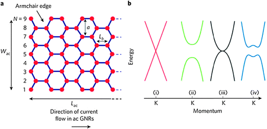 | ||
| Fig. 1 (a) Schematic demonstration of an armchair GNR. (b) Band structure near the K point of (i) bulk graphene, (ii) graphene nanoribbons, (iii) bilayer graphene, and (iv) bilayer graphene in an applied perpendicular electric field. (Reproduced with permission from ref. 8, Copyright 2010, Nature Publishing Group.) | ||
Theoretical studies have predicted that confinement of charge carriers in quasi-one-dimensional (Q1D) nanoscale systems will open a bandgap,11 and that the band gap of graphene nanoribbons (GNRs) is inversely proportional to the ribbon width (Fig. 2a). As Q1D materials, GNRs are especially interesting due to their compatibility with nanoelectronics, and their possible applications such as optoelectronics and sensors. In graphene nanoribbon field-effect transistors (GNRFETs), the logarithm of on/off current ratio is proportional to the ribbon width (Fig. 2b); this relationship is regarded as evidence of the opening of a band gap.12
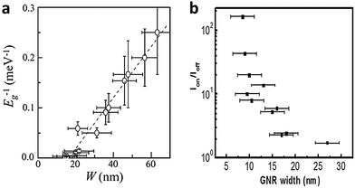 | ||
| Fig. 2 (a) Reciprocal of bandgap Eg as a function of the GNR width W. (Reproduced with permission from ref. 18, Copyright 2007, The American Physical Society.) (b) Correlation between on/off current ratio and GNR width. (Reproduced with permission from ref. 12, Copyright 2009, The American Chemical Society.) | ||
1.2. Basic properties of GNRs
GNRs are usually classified into armchair (A-GNR) and zigzag (Z-GNR) morphologies depending on the edge structures. The characteristics of the two types of GNRs differ. Theoretical studies have predicted that A-NRs and Z-GNRs will have a band gap that is inversely proportional to the ribbon width.13,14 However, the studies disagree about whether Z-GNRs can have a direct bandgap. Predictions also suggest that the edge structure will affect the magnetic properties: A-GNRs are expected to be nonmagnetic, but Z-GNRs could have a large magnetoresistance.13,15–17The correlation between the bandgap and the width of a GNR was experimentally proven for the first time by Kim et al. in 2007.18 Lateral confinement of charge carriers induced the formation of a bandgap. The bandgap was strongly correlated with the width W of the GNR (Fig. 2a). However, no clear relationship between electrical characteristics and crystallographic orientation was observed in GNRs produced using e-beam lithography. Lithographic approaches usually produce disordered edges, which may influence the electrical properties of GNRs. Anderson localization has been predicted to induce a bandgap in GNRs (both A and Z) that have disordered edges.19,20 If the edges of a GNR are not very rough, the bandgap of the GNR can be roughly estimated as Eg ≈ α/W, where α is a fitted constant.21–23
1.3. Some techniques for GNR fabrication
Numerous research papers have presented approaches to produce GNRs and to study their electrical and photonic properties for future industrial applications (Table 1). The following section describes some techniques to produce narrow GNRs (Fig. 3).| Methods | GNR width | Edge | Mobility (cm2 V−1 s−1) | I ON/IOFFa | E g (meV) | Ref. |
|---|---|---|---|---|---|---|
| a I ON/IOFF at RT if not specifically noted. b Synthesized from perianthracene. c Synthesized from perinaphthalene. d Synthesized from peritetracene. e Armchair edges produced in Ar-RIE. f An ION/IOFF of ∼3000 was achieved in a vertical electrical field for a bilayer GNR. | ||||||
| E-beam litho. | 14–100 nm | N/A | N/A | >103 (49 nm, 1.7 K) | 200 (15 nm) | 19 |
| 20 nm | N/A | N/A | >100 (4 K) | ∼30 | 33 | |
| 12 nm | N/A | N/A | 10 (300 K); 106 (4 K) | 100 | 34 | |
| 10 nm | <0.35 nm | 800–1000 | 106 (4 K, 10 nm) | 140 | 35 | |
| 5 nm | (RMS) | (10 nm) | 300 | |||
| 5 nm | N/A | N/A | 47 (RT); 105 (5.4 K) | 145 | 36 | |
| Helium beam lithography | 5 nm (min) | N/A | N/A | 2.25 (RT) | >88 | 42 |
| 6 nm (device) | 4.75 (77 K) | |||||
| Dip-pen lithography | 25 nm | N/A | 2740 (h) 3150 (e) | N/A | N/A | 46 |
| STM | 10 nm | Armchair or zigzag | N/A | N/A | 0.18 | 47 |
| 2.5 nm | 1.2 | |||||
| 1.7 nm | ||||||
| Chemical synthesis in solution or on crystalline terraces | 7, 9, 11 units | Armchair | N/A | N/A | 1.6; 0.7; 0.2 | 51 |
| 9 nm; 5 nm | 100–200 | 105 (9 nm); 106 (5 nm) | ≤400 | 21 | ||
| 7, 13 units | Armchair | N/A | N/A | 2.8 ± 0.4; 1.6 ± 0.4 | 52 | |
| Chevr.-type | 3.1 ± 0.4 | |||||
| 4 units | Armchair | 10−5; 10−4; 10−6 | N/A | 1.6b; 0.8c; 1.3d | 53 | |
| 7 units | Armchair | N/A | N/A | 2300 | 54 | |
| 7 units | Armchair | N/A | N/A | N/A | 55 | |
| ∼2 | N/A | ∼200 | >106 | N/A | 56 | |
| 13, 7 units | Armchair | N/A | N/A | 1400; 2500 (13, 7 units) | 57 | |
| 1 | Armchair | N/A | N/A | 1300 | 58 | |
| 0.74 | Armchair | N/A | 3.63 × 10³ (77 K) | 1250 | 59 | |
| 2 | N/A | N/A | N/A | 1240 | 60 | |
| 6 | Armchair and zigzag | N/A | N/A | 1400 | 61 | |
| 0.69–1.13 | Cove-type | 150–15![[thin space (1/6-em)]](https://www.rsc.org/images/entities/char_2009.gif) 000 000 |
N/A | 1880 | 62 | |
| 1.2–3.4 | Chlorinated | N/A | N/A | 1700 | 63 | |
| 1.1–0.7 | Cove-type | N/A | N/A | 1840 | 64 | |
| <2 nm | Zigzag | N/A | N/A | N/A | 65 | |
| 5 units | Armchair | N/A | N/A | 2800 ± 100 | 66 | |
| Around NWs | 200–500 nm | N/A | 70 | |||
| SiC-step template | ≤40 nm | N/A | 900–2700 | 10 (RT); >25 (4 K) | N/A | 76 |
| Ni nanostructure | 23 nm | N/A | N/A | 16 (RT); 104 (13 K) | 58.5 | 11 |
| 20 nm | N/A | >1000 | 2 | 50 | 78 | |
| Lattice oriented | <10 nm | Armchair <0.5 nm | N/A | ∼100 (max) | N/A | 81 |
| 20–30 nm | Zigzag | N/A | N/A | N/A | 87 | |
| DNA assisted | <10 nm | N/A | 0.21 | 100–500 (RT) | N/A | 88 |
| Unzipping of CNTs | >100 nm | Oxidized | N/A | <2 | N/A | 91 |
| 22–26 nm | Oxidized | N/A | N/A | N/A | 92 | |
| 130–250 nm | Non-oxidized | N/A | N/A | N/A | 93 | |
| 2.8 nm | Zigzag dominant | 1800 | <2 | N/A | 94 | |
| <10 nm | Smooth | N/A | >10 (7 nm) >100 (6 nm) | N/A | 95 | |
| 10–20 nm | N/A | 1500 | 4.5 (RT); 10 (20 K) | 10–15 | 96 | |
| 4–26 nm | Armchair and zigzag | N/A | N/A | N/A | 97 | |
| 2–8 nm | Smooth | N/A | N/A | N/A | 98 | |
| BCP self-assembly | 9–12 nm | N/A | 120 (e) 60 (h) | 100 (100 K) | 58 (12 nm); 8 (9 nm) | 108 |
| ∼12 nm | N/A | N/A | <2 | N/A | 109 | |
| ∼10 nm | N/A | N/A | N/A | N/A | 110 | |
| 8 nm | ∼2.4 nm (3σ) | 25 | 13 (RT) | N/A | 111 | |
| Edge-narrowing | Sub-5 nm | ≤5 nm | N/A | 104 (RT) | 400 | 113 |
| ALD-on edge | 15 nm | N/A | ∼400 (15 nm) | ∼4 | N/A | 118 |
| Meniscus mask | 6.4 nm | Armchaire | 14 (h+) | 10 (RT); 103 (5 K) | 120 | 119 |
| Barrier-guided | 25 nm | N/A | 215 | ∼6 | 15 | 120 |
| i-NW lithography | 8 nm | N/A | 160 | 12 | ||
| 50–100 nm | N/A | 1200 | 13–51 | 130 | ||
| 15 nm | N/A | 1300 | 12 | 131 | ||
| 10 nm | N/A | 70 | 134 | |||
| 40 nm | N/A | 3000f | 138 | |||
| 6 nm | N/A | 143 | ||||
| e-NW lithography | 9 nm | N/A | 300 | 70 | 100 | 160 |
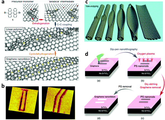 | ||
| Fig. 3 Some techniques to fabricate GNRs. (a) Chemical synthesis from selected monomers. (Reproduced with permission from ref. 51, Copyright 2010, Nature Publishing Group). (b) STM lithography. (Reproduced with permission from ref. 47, Copyright 2008, Nature Publishing Group). (c) Unzipping of GNTs. (Reproduced with permission from ref. 91, Copyright 2009, Nature Publishing Group). (d) Dip-pen nanolithography. (Reproduced with permission from ref. 46, Copyright 2011, Nature Publishing Group.) | ||
Theoretical studies have suggested that the orientation of a GNR may influence its electrical properties. However, no obvious correlations have been observed; this result implies that the edge structure has a stronger influence on the properties of a GNR than does crystallographic orientation.
Other theoretical work has suggested that Eg is influenced by atomic structures on the edges of GNRs.13,15,25–32 No obvious dependence of electrical characteristics on crystallographic orientation has been observed; this result indicates that e-beam lithography did not achieve precise control of the edges of the GNRs.
Other groups also used e-beam lithography to fabricate GNRs.33–36 Hwang et al. used e-beam lithography34 with methylisobutylketone (MIBK)-diluted HSQ as an e-beam resist and a CVD-grown graphene sheet that was transferred to a 90 nm-SiO2-coated p+Si wafer for patterning; they produced GNRs with W = 12 nm (Fig. 4a). The 12 nm-wide GNR was connected to a graphene contact pad through a linear lithographic flare to achieve a continuous change of the GNR bandgap to the zero bandgap of bulk graphene electrodes (Fig. 4b). The RMS roughness of the GNRs was ∼0.35 nm. Ambipolar charge transport was observed in the device. GNRFETs had an on/off current ratio ION/IOFF of ∼10 at RT and this was as high as 106 at 4 K (Fig. 4c). A bandgap of ∼100 meV was calculated by using a differential conductance method to evaluate the GNRFETs (Fig. 4d).
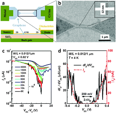 | ||
| Fig. 4 E-beam lithography to produce graphene nanoribbons (GNRs). (a) Schematic illustration of the configuration of a GNRFET. (b) SEM image of a GNR (inset: magnified view of the nanoribbon with a width of 12 nm). (c) Transfer curves of the 12 nm wide GNRFET at various temperatures. (d) Differential and absolute drain current vs. drain voltage (Vg ∼ 50.5 V). (Reproduced with permission from ref. 34, Copyright 2007, AIP Publishing.) | ||
Although EBL can produce GNRs with precise positioning, it is a high-vacuum, time-consuming serial process, so it is not amenable to scale-up for industrial-scale production. EBL also has resolution limitation that hinders the production of GNRs with width < 10 nm, which are usually required for the formation of a sufficiently large band gap for RT applications. Another drawback is that the etching process causes damage, so atomically smooth level edges are not achievable, and this process also produces numerous dangling bonds and chemical functional groups on the edges of GNRs; as a result, their electrical properties are degraded. Another drawback is that the resist leaves residue that is difficult to remove completely.
The ability of HIBL to precisely control W down to 5–6 nm revealed on-current degradation as the feature size of GNRs was reduced. Compared to a bulk graphene sheet, the current density was decreased to ∼1/2 in a 15 nm-wide GNR and to ∼1/5000 in a 6 nm-wide GNR.42 In a separate study, the carrier mobility of a 15 nm-wide GNR was 1/15th that of a 1000 nm-wide GNR.43 The degradation of carrier mobility can be attributed to several causes: (1) the edge scattering effect that is inversely proportional to W; (2) dangling bonds as surface defect states that form when Si–O bonds break during etching; (3) increased effective electron and hole masses as GNRs become narrow;42,44 (4) charge traps produced in SiO2 during etching.
Although the above techniques can produce individual GNRs with W < 10 nm, additional requirements must be satisfied before industrial applications are practical. These requirements include alignment ability, uniform control over W, a high AR, and edge roughness. The development of scalable approaches to synthesize graphene has enabled fabrication of GNR circuits on a large area; examples include epitaxial graphene sheets on the SiC surface,48,49 and CVD growth on catalytic metal surfaces.6,50
Previous review papers about GNRs have summarized the fabrication techniques and the properties of GNRs. However, for real application, fabrication and alignment of GNRs on a large area is essential. The main focus of this paper is to review methods for large-scale fabrication of GNRs, especially those that have shown potential for fabrication of GNRs on a large area with individual control of position and alignment. At least three criteria of GNR fabrication are required for practical application: (1) fabrication of GNRs with W < 10 nm, (2) direct integration to insulating or semiconducting interfaces, and (3) mass production of GNRs with individually controlled position and alignment. Efforts have been made to overcome these challenges.
2. Current techniques that show potential for large-scale fabrication of GNRs
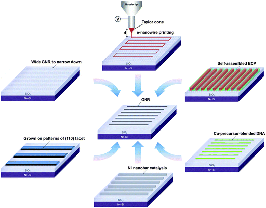
Some approaches have shown potential for large-scale fabrication of GNRs with controlled alignment (Fig. 5 and Table 1), which will be discussed in the following sections.2.1. Bottom-up organic synthesis method in solution
GNRs can be chemically synthesized from various monomers.21,51–69 The W and edge types (i.e., A or Z) can be defined with atomic precision by designing the structure of precursor monomers. Chemically derived GNRs usually have uniform edges. A very narrow (down to 7 C-atoms wide) W can be obtained with good control. The first graphite nanoribbons were synthesized in solution.67 The synthesis is generally based on solution-mediated cyclodehydrogenation and “planarization” of three-dimensional polyphenylene precursors. The polyphenylene precursors are designed and synthesized from small organic molecules, and provide the ability to fabricate GNRs with different widths and edge structures.68 Recently, GNRs with L > 600 nm have been produced using this bottom-up organic synthesis in solution,62 and large-scale solution synthesis of narrow GNRs has also been achieved using this method.58 The bottom-up organic synthesis method in solution has been well developed and serves as an indispensable tool to create structurally defined GNRs. In contrast to the “top-down” methods, “bottom-up” organic synthesis in solution provides structurally well-defined GNRs with uniform structures. However, the synthesized GNRs must be transferred to suitable substrates with precise position control; this requirement is a difficult challenge.Atomically controlled substitutional doping of GNRs can also be achieved using chemical synthesis in solution. Desired elements for either p- or n-doping can be designed in the monomer for the GNR synthesis, so that these elements are incorporated into the synthesized GNRs.69 Although atomically controlled doping of GNRs on a large-scale is difficult at this time, this method provides a practical way to achieve an efficient band gap for GNRs, and could direct future development of this research field.
2.2. Templated bottom-up growth
Bottom-up growth avoids etching over GNR edges, and thereby maintains physically smooth and chemically clean edges. This process yields high-quality GNRs, which usually possess higher charge-carrier mobility than that achieved using top-down approaches. The critical step is to obtain pre-patterned catalytic nano-patterns; this goal can be realized by using catalytic edges of thin metal films, or by using other techniques.Early attempts at bottom-up growth of GNRs used Pd nanowires to catalyze the growth of GNRs as surroundings.70 The Pd NWs can then be removed to achieve edge-closed GNRs, or if the top-layer graphene ribbons are etched away by oxygen plasma before the removal of Pd nanowires, edge-open graphene ribbons can be achieved. However, the alignment of individually addressable i-NWs is still a difficult challenge. This technique is very useful for scientific research, but is not suitable for mass-production of addressable GNRs on a large area.
Sprinkle et al. exploited this phenomenon to design an approach for bottom-up growth of GNRs (Fig. 6a).76 Nickel lines were first fabricated on a flat SiC surface by photolithography followed by fluorine RIE. The edge line patterns of the Ni mask were then transferred to the underlying SiC. This very easy process controlled the etch depth accurately on a nanoscale. The lithographic depth determined the final width of GNRs (Fig. 6a): a 20 nm lithographic depth yielded 40 nm-wide GNRs, which could be further narrowed by decreasing the lithographic depth. The crystal was heated at 1200–1300 °C in vacuum after removal of the Ni mask to form a SiC step flow. The abrupt step relaxed into a (110) facet. The temperature was increased to 1450 °C after 1.5 min to induce selective growth of GNRs on this nanofacet.71–73
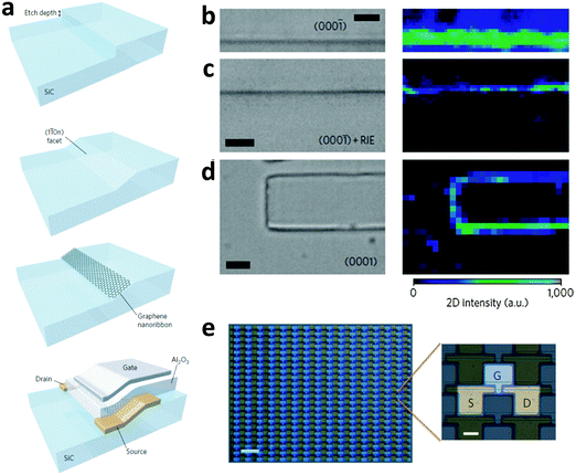 | ||
| Fig. 6 (a) Fabrication of a nanometer-wide step on SiC and growth of GNRs on it, and the fabrication of a top-gated GNRFET. Optical micrographs and Raman mapping images of (b) a 100 nm-wide step of the (000−1) facet after graphene growth, (c) the (000−1) facet after graphene growth and oxygen plasma exposure, and (d) selective growth on SiC without post-treatments (scale bar for left images in (b), (c), and (d): 2 μm). (e) Optical micrograph of GNRFET arrays; scale bar: 100 μm (left) and 20 μm (right). (Reproduced with permission from ref. 76, Copyright 2010, Nature Publishing Group.) | ||
Careful control of the temperature, time and atmosphere during CVD growth induces selective growth of GNRs on the facets (Fig. 6b–d). Raman mapping over a 100 nm SiC step and adjacent facets confirmed the existence of graphene at the step edges by showing strong 2D bands (2700 cm−1) there, but found almost none on the horizontal surfaces. Raman spectroscopy, HR-TEM and EFM confirmed the growth of 40 nm GNRs at expected positions. The GNRs exhibited the quantum confinement effect at 4 K. Electronic devices based on these GNRs showed an RT ION/IOFF of ∼10 and a charge carrier mobility of ∼2700 cm2 V−1 s−1. High-density transistor arrays were fabricated (Fig. 6e). The technique could be further refined by downscaling GNR width, or by selecting different gate dielectrics and crystallographic facets. The bottom-up growth avoids the generation of side defects during cutting by plasma. The GNRs show metallic behavior at relatively high temperature, but quantum confinement at 4 K. Reduction of the width to ∼40 nm yields a bandgap at RT.77
2.2.2.1. Growth on nickel nanobars. Ni is a well-known catalytic metal substrate for multi-layer graphene growth. Therefore, Ni nanostructures should be evaluated as a bed for GNR growth. Kato et al. reported direct growth of GNRs from pre-patterned Ni nanostructures (Fig. 7a).11 In this approach, Ni nanobars with width 50–100 nm, height 35–85 nm and length 200–5000 nm were pre-patterned using conventional e-beam lithography and then connected to two Ni electrodes as the source and drain. Rapid-heating plasma CVD (RH-PCVD) was then applied to these nanostructures, and the patterns were directly converted to GNRs. The sacrificial Ni nanobars were partially or fully eliminated during the growth of GNRs. The keys to this direct conversion process are rapid heating, abundant supply of hydrocarbon sources, and relatively thin Ni nanostructures. During growth, the narrowest Ni structures were volatilized to leave GNRs in the channel region, but the Ni electrodes remained. Due to elimination of the Ni structures, the GNRs are usually ∼23 nm narrower than their sacrificial catalytic nanostructures (Fig. 7b). The conversion efficiency was 45–70%. The large height of ∼60 nm suggested a suspended structure of the GNRs. TEM revealed clear graphitic lattice structures with 0.34 nm spacing and a multilayer graphene sheet with 5–10 layers of graphene. The bottom-up growth avoids lithographic approaches, so it produced GNRs with relatively flat and smooth surfaces and edges. Complex architectures such as multichannel structures and radical line structures are achievable by designing the patterns of the Ni nanostructures. During RH-PCVD, only the narrowest parts of Ni were converted to GNRs; this trait can be used to ensure that GNRs grow only at specific points in a pre-constructed structure.
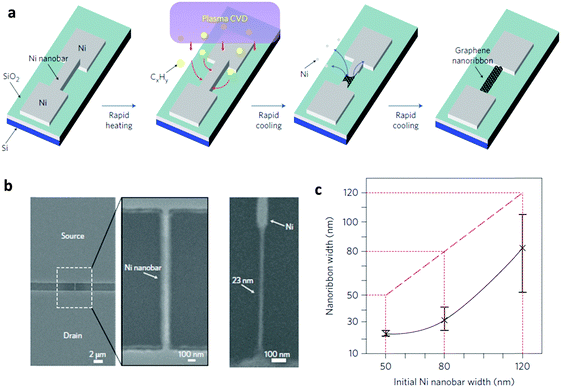 | ||
| Fig. 7 (a) Schematic of the site- and alignment-controllable fabrication of GNR arrays from nickel nanobars. SEM images of (b) a nickel nanobar and a GNR. (c) Correlations between nanoribbon width and the initial width of the nickel nanobar. (Reproduced with permission from ref. 11, Copyright 2012, Nature Publishing Group.) | ||
Although the site and alignment of GNRs can be controlled, this process still has the limitation that patterning of the Ni nanostructures requires e-beam lithography, so the problems involved with a serial, time-consuming, and high cost process remain. Due to the resolution limitation in patterning Ni nanostructures, the narrowest GNR width was ∼23 nm.
2.2.2.2. Growth on the edge of nickel thin films. Controlling the thickness of a catalytic metal thin film is probably much easier than laterally confining the width of a nanostructure, because a nanoscale thickness of the film can be easily obtained during the deposition process. This is a possible solution to avoid the e-beam lithography approach to achieve a nanostructured Ni catalytic layer (Fig. 8a).78
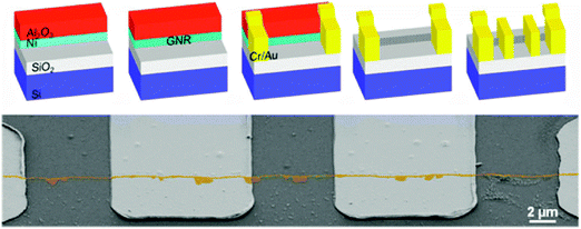 | ||
| Fig. 8 (a) Schematic of vertical GNR growth on the edges of thin Ni layers with an Al2O3 passivative layer on top and a GNRFET. (b) SEM image of GNRs with electrodes. (Reproduced with permission from ref. 78, Copyright 2012, The American Chemical Society.) | ||
A 20 nm Ni thin layer is first deposited on a SiO2-coated highly doped silicon wafer and then coated with 75 nm Al2O3 as a protective layer. The double layer thin film is then patterned to leave laterally exposed nanoscale Ni edges with desired patterns. Vertical GNRs with height ∼20 nm were achieved (Fig. 8b). A planar Ni nanostructure is difficult to pattern, but the thickness of the Ni layer can be easily controlled during the deposition process, if an inert protective layer is applied to cover the Ni layer. This is a method to grow vertical GNRs.
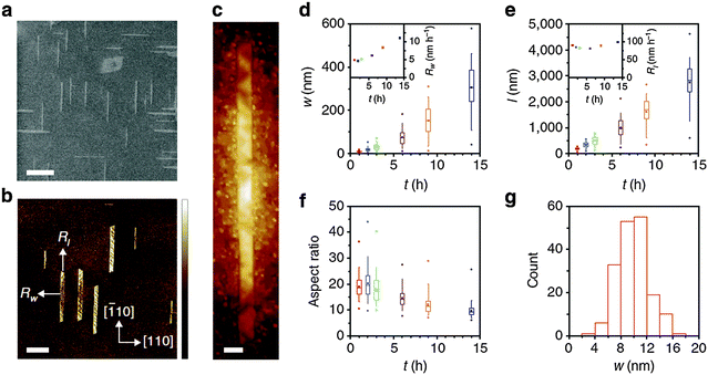 | ||
| Fig. 9 (a) SEM (scale bar: 400 nm), (b) AFM (scale bar: 400 nm) and (c) STM images (scale bar: 10 nm) of GNRs grown on Ge(001). (d) Width, (e) length and (f) aspect ratio of GNRs as a function of growth time. (g) Histogram for the distribution of GNR width. (Reproduced with permission from ref. 81, Copyright 2015, Nature Publishing Group.) | ||
Anisotropic growth of GNRs was achieved on Ge(001) by controlling CVD conditions such as temperature, fractions of CH4 and H2 and growth time. The key to this anisotropic growth is to use growth with a very restricted rate < 5 nm h−1. Under optimized conditions, the separated GNRs could be allowed to grow preferentially for >18 h, whereas thin film growth on Ge(001) was completed in <100 min.79
The anisotropic growth was due to selective attachment of hydrocarbon intermediate products to short edges rather than to the long ribbon edges. As a consequence, the GNRs grew preferentially in the length direction, and therefore elongated instead of widening. During the growth process, the energy barrier for the intermediate products to attach to the long ribbon edges was determined by the relative positions of GNR edges to Ge steps; this process is similar to the formation of polygonal graphene crystals82 and of Q1D structures on zinc-blende semiconductor (001) facets.83–85 However, the barrier for the attachment of intermediate products decreased once GNRs overgrew the Ge steps; furthermore, W increased rapidly when it exceeded 30 nm. The subsequent rapid growth was due to the GNRs exceeding the steps on the Ge surface and thereby overcoming the attachment barrier.
Direct, definable growth provides precise control over GNR growth, and can produce relatively pristine GNR/substrate interfaces. This type of GNR has W < 10 nm, a high AR and very smooth armchair edges. These characteristics indicate that these techniques can be adapted to realize mass production and high yield to directly integrate GNRs into conventional semiconducting wafer platforms.73,86 Similar approaches that use surficial lattice structures to orient the growth of GNRs have also been reported.87
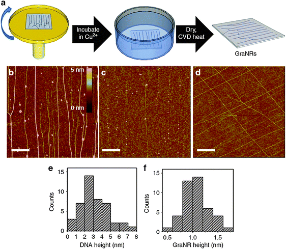 | ||
| Fig. 10 (a) Schematic of the DNA-template production and its conversion to GNRs. AFM images of (b) stretched DNAs, (c) GNRs and (d) cross-shaped GNRs (scale bar: 1 μm). Histograms of the heights of (e) DNAs and (f) GNRs. (Reproduced with permission from ref. 88, Copyright 2013, Nature Publishing Group.) | ||
2.3. Unzipping carbon nanotubes
Carbon nanotubes (CNTs) have many similarities to graphene, such as the nanoscale width and Q1D structure. A CNT can be unzipped longitudinally to produce a GNR. Single-walled CNTs can be converted to single-layer GNRs, and multi-walled CNTs can be converted to multi-layer GNRs.91–98 The unzipping can be achieved using chemical approaches and controllable RIE etching approaches to partially remove some top parts of a CNT to leave a GNR. Wet chemical reactions and dry etching processes have both been used successfully.Kosynkin et al. reported an oxidation process in solution to cut multiwalled carbon nanotubes (MWCNTs) lengthwise.91 This process yielded nearly 100% GNR structures with high water solubility. Due to the existence of abundant oxygen-containing functional groups on the surface, the conductivity of the as-produced GNRs was not good. The conductivity can be improved by subsequent chemical reduction by N2H4 or annealing in H2.
Liao et al. reported a gas-phase plasma etching process to convert masked CNTs to GNRs.95 High-quality, narrow GNRs were produced using the approach.96 The same group then suggested a two-step process to unzip nanotubes for mass production of high-quality GNRs. Mild calcination at 500 °C in air induced oxidation of pre-existing defects to produce pits on the side walls of CNTs, and then sonication in organic solvents effectively enlarged the pits and unzipped the CNTs to form GNRs. The GNRs were then purified by ultracentrifugation. Narrow GNRs with a width of 10–30 nm were generated. CNTs have also been unzipped by catalytic cutting99 and pulse-burning at high current.100
As strategies for scalable fabrication of uniform CNTs and their alignment are being developed, the synthesis of GNRs by longitudinal unzipping of CNTs is also becoming a promising approach to achieve mass production of GNRs. Further improvement of the strategy could include synthesizing GNRs of uniform W with narrow W distribution, of defined edges with specific chirality, and of fixed number of cylinders.
2.4. Block-copolymer lithography
Block copolymers can self-assemble into various nanostructures, such as spheres, cylinders, lamellae, vesicles, and many other complex or hierarchical assemblies.101 The nanostructures can have a feature size between 10 nm and 100 nm, depending on the design of the blocks and the number of monomer units. Benefiting from this tailorable feature, block copolymers have been widely used in nanotechnology, e.g., as lithographic tools in the semiconductor industry.102–105 Recently, block-copolymer templates have been used to produce GNRs.106–109Self-assembled block copolymers have been used as etch masks to convert their patterns to graphene for fabrication of GNR arrays.106–109 Some early efforts include the production of 12 nm-wide GNRs107 and sub-10 nm GNRs by controlling the number of brush layers and etching time,108 but either no obvious change was observed between the GNRs and graphene flakes or no electrical characteristics were reported. Polystyrene-block-polydimethylsiloxane (PS-b-PDMS) is a block copolymer with a very high Flory–Huggins interaction parameter, which ensures very small periods. Complex patterns from PS-b-PDMS self-assembly are also attainable.110 These properties make the block copolymer suitable for the fabrication of highly aligned sub-10 nm grating patterns.109,111
Liang et al. fabricated GNR arrays with half-pitch < 10 nm by using a nanofabrication approach that combines nanoimprint lithography and self-assembled templates of block copolymers.109 CVD-grown graphene monolayers that were transferred onto a 300 nm-SiO2-coated p+Si wafer were used as the matrix for patterning.
A poly(styrene-b-dimethylsiloxane) (PS-b-PDMS) block copolymer thin layer was spin-coated and then annealed at favorable temperature. Phase separation during annealing yielded PS and PDMS nanoscale domains (Fig. 11). Nanostructured single-layer PDMS cylinders with diameter < 10 nm were formed, which were surrounded by PS.112 The PS component was easily removed by a brief oxygen plasma treatment to leave PDMS cylinders to serve as etch masks that attach to the underlayer. Directional CF4/O2-based RIE was used to remove the unprotected cross-linked polymer and underlying graphene. GNRs with W < 10 nm were formed. Over-etching cleaned up the remaining directing structures and underlying graphene between the GNRs.
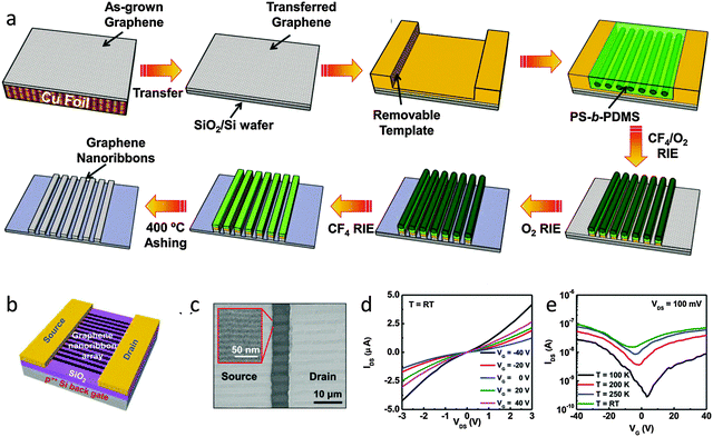 | ||
| Fig. 11 (a) Schematic of processes to fabricate self-assembled PS-b-PDMS patterns and graphene nanoribbons. (b) Schematic of a multi-channel GNRFET. (c) SEM image of the channel region of the GNRFET with a magnified image of the GNR arrays. (d) Output and (e) transfer curved of the GNRFETs. (Reproduced with permission from ref. 106, Copyright 2013, Wiley-VCH Verlag GmbH & Co.) | ||
Multi-channel FETs with ∼50 GNRs showed an improved ION/IOFF > 10, which indicates that a bandgap opened in the densely arranged graphene nanoribbons. The ION/IOFF was significantly affected by the standard deviation of the width of GNRs in the multi-channel device geometry. The block copolymer self-assembly could be controlled by altering the processing conditions, and this approach could be used to control the standard deviation of the width of GNRs.
High-density and uniform GNRs on a large area with half-pitch < 10 nm were produced by combining directed self-assembly of block-copolymers and nanoimprint lithography.109 The GNRs were used as active channels in multichannel field-effect transistors. The large variation in the width of the ribbons in the multichannel devices could cause switching behaviors to lose synchrony, and thereby result in a poor ION/IOFF. GNRs with half-pitch = 8 nm were produced. The minimal ribbon-to-ribbon width variation was ∼2.4 nm (3σ value). An ION/IOFF > 10 was achieved at RT; this result suggests that a bandgap opened in the GNR arrays. The ION/IOFF was among the highest values of GNRFETs with dense GNR arrays as active channels at the time.
Son et al. developed a PS-b-PDMS template that self-assembled into cylindrical segregating morphology, and then used the template as a lithographic tool for patterning CVD-grown graphene.106 They also used a transferred graphene sheet that had been grown using copper-catalyzed CVD. GNRs were produced with width in the range of 9–12 nm, and their field-effect and photoelectrical characteristics were also evaluated. The ION/IOFF was higher in the GNR arrays than in the graphene sheet, and was strongly dependent on temperature. GNR arrays generated 30 times more photocurrent than did a bulk graphene sheet; this difference indicates that GNRs have semiconducting properties, and further confirms that a band gap opened. Compact GNR arrays would help realize large-area graphene electronics.
The fabrication of multichannel GNRFETs using BCP lithography helps to understand the relationship between uniformity of GNRs in an array and the ION/IOFF of a multichannel GNRFET. BCP-template lithography provides a practical strategy to produce densely aligned GNR arrays with half-pitch < 10 nm, which are desirable in future nanoelectronics.
2.5. Narrowing of GNRs from edges
Another strategy to produce GNR arrays is to narrow GNRs from the edges. Wang et al.113 used conventional lithographic approaches to fabricate ∼20–30 nm-wide GNR arrays by electron-beam lithography, and then used gas-phase reactions to narrow them. Under optimized conditions, GNRs could be uniformly etched from edges; the authors suggested that this uniformity is due to the presence of functional groups and band disorders at the edge carbons, which are more chemically reactive than those within the plane.114 GNRs produced using e-beam lithography (∼20 nm) were etched from edges at a rate of 0.51 nm min−1 (25 mTorr O2 in 1 Torr NH3/Ar at 800 °C). The etching process involves O2 oxidation of carbons into gaseous products, e.g., CO2 and CO. The C atoms at edges and defect sites preferentially react with O2 molecules.115,116 The NH3 atmosphere contributed to slow down the etching rate during oxidation,117 because NH3 is efficient in reducing oxygen groups in graphene oxide, so reduction by NH3 could slow down the oxidation of graphene from edges.Using this approach, GNR arrays with width ≤ 5 nm were produced. GNRFETs in which GNRs were used as active channels achieved a very high ION/IOFF of ∼104 at RT; this is further evidence that a band gap opened. GNRFETs in which the active channel consisted of parallel arrays of ∼8 nm-wide GNRs were also fabricated and showed an ION/IOFF of ∼50 and a much higher ‘on’ current than did single-ribbon devices. This technique provides an important route to realizing large-scale integrated circuits based on GNRs.
2.6. Protection at edges
MML is an efficient top-down approach to produce GNRs with W < 10 nm and high AR; it is also scalable. By exploiting the mechanism of the technique, GNRs with an arbitrary configuration can be produced. The process does not use high-resolution lithography tools. The use of Ar-RIE ensures the production of armchair edges of GNRs and consistent electronic properties in the resulting devices. Extended applications of the technique could include fabrication of nanostructures of diverse materials.
2.7. Barrier-guided growth
Arnold's group proposed barrier-guided chemical vapor deposition (BG-CVD) of micro- and nano-structured graphene.120 In BG-CVD, a barrier material (i.e., 10 nm alumina) is placed on a catalytic substrate to restrict the graphene growth to desired regions. Alumina was selected as the barrier material due to its low C solubility, high thermal stability and chemical inertness to both C and Cu.121 During subsequent CVD, the selective coverage of inert oxide caused methane to decompose selectively on uncovered Cu surfaces, and due to the low solubility of C in Cu,122 C cannot diffuse under alumina. Selective growth was ensured by the inertness of oxide and by a strong Cu–C bonding energy of ∼5 eV.123 After the processes of nucleation and lateral growth to cover the fully exposed Cu surface, graphene growth terminated. The patterned graphene produced by BG-CVD on the Cu substrate can be transferred to arbitrary substrates with the assistance of surface-coated supporting polymers.BG-CVD is a bottom-up growth approach to laterally guided synthesis of graphene. Highly crystalline, rationally patterned micro- and nano-structured graphene were produced. In contrast to lithography approaches, high quality edges are expected.
2.8. Nanowire lithography
Bai et al. reported the first use of i-NWs and an etch mask to produce GNRs (Fig. 12a).12 Si i-NWs were grown using a nanocluster-mediated vapor–liquid–solid growth approach and then placed on top of graphene by using an AFM tip (Veeco Dimension 5000). The samples were dipped into isopropyl alcohol to introduce capillary force to ensure tight contact and then dried under blown N2. The samples were then exposed to O2 plasma to selectively remove the unprotected part of graphene and leave GNRs beneath the i-NWs, which served as protective masks against RIE etching. The initial etching was nearly anisotropic to transfer the shadow to GNRs; extended O2 plasma exposure further narrowed the width by causing lateral etching of the shadowed area that was not in direct contact with the underlying graphene. GNRs with width from 30 nm down to 6 nm were produced in this way. The protective i-NWs can be easily removed by brief sonication. This approach of using chemically synthesized inorganic nanowires as etch masks allows rational fabrication of GNRs. GNRs with width < 10 nm were obtained; they had a band gap of 100 meV. FETs that used the GNR as the active channel had a ION/IOFF of ∼150. Similar approaches were developed subsequently.130
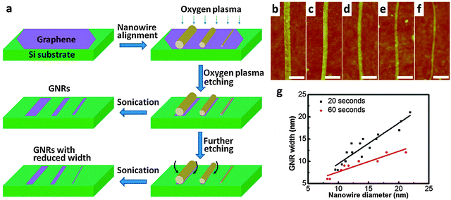 | ||
| Fig. 12 i-NW lithography. (a) Schematic demonstration of the nanowire lithography process using nanowires with various diameters for the fabrication of GNRs with various diameters. (b–f) AFM images of the produced GNRs with width from 31 nm to 6 nm. Scale bars: 100 nm. (g) Correlations between GNR width and nanowire diameter for GNRs produced by oxygen plasma treatment for 20 s (black) and 60 s (red). (Reproduced with permission from ref. 12, Copyright 2009, The American Chemical Society.) | ||
The simple use of an insulating i-NW etch mask as a gate insulator was demonstrated by Liao et al.131 They used thermally grown zirconium oxide (ZrO2) nanocrystals with lengths of several tens of micrometers and diameters of 40–100 nm. ZrO2 has a wide bandgap (5.1–7.8 eV) and a high dielectric constant, and is a good gate insulating material in FETs.132,133 The ZrO2 i-NWs were physically transferred to the graphene surface by contact printing and then aligned using shear force during a sliding process. Capillary force was then introduced to form close contact between ZrO2 i-NWs and graphene. A long RIE etching time of 160 s at 40 W was used to achieve severe lateral etching to leave narrow GNRs. 50 nm-diameter i-NWs usually produce an underlying 15 nm-wide GNR. A later-deposited electrode that was not in contact with the GNR served as a gate electrode. An RT ION/IOFF of ∼12 was calculated from the transfer curves at a drain voltage of ∼0.1 V (Fig. 12b). The device can be evaluated either as a bottom-gated transistor insulated by SiO2 or as a top-gated device insulated by ZrO2 NW. Compared with a bottom-gated device, the use of a high-k i-NW gate insulator significantly reduced the operating voltage from 10 V to 2 V (Fig. 12c). A high field-effect mobility of ∼1300 cm2 V−1 s−1 was achieved in the devices; this result indicates that the GNRs were of high quality and had relatively smooth edges.
The technique was further modified by using a conductive i-NW which later served as a conductive gate. An HfO2 thin layer surrounding the i-NW was then deposited, and later used as the gate insulator.134 The wide bandgap (∼5.8 eV) and high dielectric constant (∼25) made HfO2 an excellent gate dielectric.135 ALD allows deposition of a high-quality HfO2 layer as thin as 2 nm to serve as a gate insulator layer between the conductive NW and the GNR active channel; this layer allowed negligible tunneling leakage current in the device during a gate voltage sweep between −1 V and +1 V. The device had an on-current of 27 μA (at Vd = 1 V and Vg = −1 V) and RT ION/IOFF = 70 under ambient conditions; these measurements are consistent with those of a 10 nm-wide GNR.33,136
A three-dimensional finite element method was used to evaluate the capacitance of the capacitor structure of a 30 nm Si/HfO2 core/shell nanowire with a 0.5 nm SiOx core and a 2 nm HfO2 shell. The electrostatic capacitance was calculated to be 3530 nF cm−2, which is even larger than the quantum capacitance (∼2000 nF cm−2) of graphene.137 The calculated hole mobility in the GNR device was 880 cm2 V−1 s−1.
Bilayer GNRs have also been fabricated using i-NW lithography.138 This work also reported that the band gap of GNRs can be further increased by breaking the inversion symmetry of a bilayer GNR. Core/shell structured Si NWs with a 2 nm-thick Al2O3 layer uniformly coated on the surface were used as lithographic masks for GNRs. Due to the easy breakdown of the SiO2 layer after O2 plasma treatment, additional 60 nm HfO2 layers were deposited after the production of GNRs to enhance the dielectric layer. The NW lithographic bilayer GNR was thus bottom-gated with a 300 nm-thick SiO2 layer and top-gated with the Si/Al2O3 core/shell NW and the 60 nm HfO2 layer. As a bottom-gated device, the GNRFETs had an ION/IOFF of ∼10, which is similar to previous reports. This ratio was increased to 70 by breaking the inversion symmetry.
The application of a vertical electric field is probably an efficient way to further increase the ION/IOFF. The GNRFET produced using an extended etching time to narrow the GNRs showed an ION/IOFF of ∼400 at RT; the ratio was increased to ∼3000 by applying a vertical electric field. This ratio is 30 times higher than the previous record high for bilayer graphene.139
Breaking inversion symmetry by introducing a vertical electric field increases the band gap of bilayer GNRs, but not of single-layer GNRs. The difference in response occurs because the two structures have distinct bandgap structures. Although bilayer graphene has a gapless band structure with conduction and valence bands in contact at a K point, a finite band gap can be opened by applying a perpendicular electric field to the graphene plane; under this condition the conductive band moves upward and the valence band moves downward.8 The widening of the bandgap of GNRs by introducing a vertical electric field was predicted theoretically.140,141
Zhou et al. introduced the use of on-wire lithography (OWL), which is usually used to produce nanowires with nanogaps, for the production of GNRs. The approach is especially effective in producing GNRs with gaps of <10 nm.142
Compared with conventional EBL, i-NW lithography can produce GNRs with smoother edges because the resolution of the former method is limited and the latter has smooth edges of etch masks, i.e., nanowires usually have very smooth edges. Chemically synthesized i-NWs are usually used for i-NW lithography. However, this approach is only feasible for small-scale fabrication due to the difficulty in alignment; the use of this technique for mass production of GNR circuits is not currently feasible.
The inherent properties of i-NWs, such as the nanoscale width and smooth edges, qualify them for use as templates in the fabrication of GNRs. However, although this is a simple approach, the technique is usually limited by the low AR of NWs and the difficulty of aligning i-NWs after growth. Mass production of i-NWs with controllable alignment remains a difficult challenge. Even though several approaches have been proposed, they mainly showed the possibility of aligning post-synthesized NWs with a low AR, but the use of such aligned NWs as etch masks is not feasible for the production of long-continuous, digitally positioned GNRs. Mass production of GNRs using NW lithography is thus limited by the currently available techniques for i-NWs.
The electrohydrodynamic nanowire printing (e-NW) printing technique is a probable solution,159 which prints long, continuous organic nanowires with digitally controlled precision of alignment. This is realized using home-built equipment that consists of two major parts (Fig. 13a). One part is the injector, composed of a syringe pump, a syringe with a metallic nozzle and a high-voltage (kilovolt-level) supplier connected to the nozzle. This part is similar to an electro-spinning system. The other part of the equipment is a horizontally placed collector, which is electrically grounded and can move horizontally under computerized control of speed and direction. During e-NW printing, the syringe is filled with polymer solution. The syringe pump controls the injection rate of polymer solution. The organic solvent is vaporized in the high electric field and solid state e-NWs finally arrive at the collector (Fig. 13a inset).
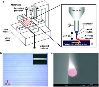 | ||
| Fig. 13 (a) Schematic of an e-NW printing system. (b) Well-aligned PVK NWs with a spacing of ∼50 μm and a diameter of 290 nm (inset, scale bar, 200 nm). (c) SEM image of the cross-sectional view of a PVK NW. (Reproduced with permission from ref. 144, Copyright 2013, Nature Publishing Group.) | ||
To successfully print e-NWs with digitally controlled patterns, special attention should be paid to the viscosity of the solution, injection rate of the solution, supplied voltage, tip-to-collector distance DTC and the moving speed and direction of the collector. The tip-to-collector distance must be optimized (e.g., 2.5 mm for PVK). If DTC is much shorter than this value, vaporization of solvents is insufficient, so the jet is still liquid when it strikes the platform. If DTC is too long, the printed NWs form coils, as occurs in the electrospinning process. At DTC = 2.5 mm, well-aligned PVK NWs are printed, with an average diameter of 290 nm (Fig. 13b, inset). The resultant electrodynamically produced nanowires (e-NWs) are perfectly circular in cross-section (Fig. 13c).
The well-aligned e-NWs can be used as etch masks of GNRs (Fig. 14). As a benefit of the digital control of the moving direction and speed of the collector, the e-NWs can be printed in various alignments including parallel lines with different pitch, grids, ladders, and stars (Fig. 15a–e). The diameter of e-NWs can be easily controlled by modulating the concentration of the polymer solution. The diameter of the e-NWs can be controlled from several hundreds of nanometers down to several tens of nanometers (Fig. 15f–j). Oxygen plasma removes the unprotected regions of graphene to transfer the patterns of e-NWs to the produced underlying GNRs (Fig. 15k–o).160–162
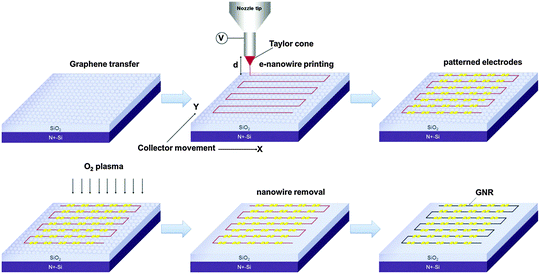 | ||
| Fig. 14 Schematic of the e-nanowire lithographic process for the fabrication of GNR arrays. (Reproduced with permission from ref. 145, Copyright 2014, Wiley-VCH Verlag GmbH & Co.) | ||
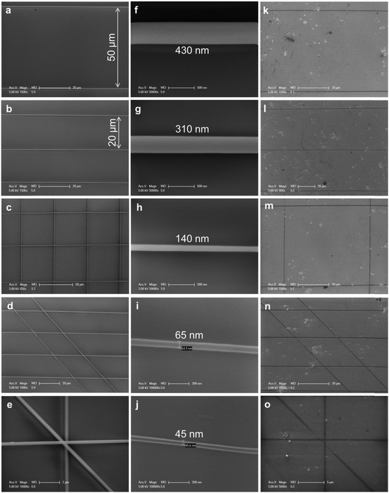 | ||
| Fig. 15 SEM images of (a–e) various patterns of PVK NWs as obtained from e-NW printing, (b) PVK NWs with various diameters from several hundreds of nanometers down to several tens of nanometers, and (c) GNR patterns as etched from the PVK NW masks of (a–e). (Reproduced with permission from ref. 145, Copyright 2014, Wiley-VCH Verlag GmbH & Co.) | ||
The various alignments of the e-NWs can be used as etch masks on graphene to transfer these patterns to the produced GNRs. Due to the perfectly circular cross-section of the e-NWs, the contact between the e-NW and the underlying graphene is very narrow. An extended etch time causes isotropic, lateral etching of shadowed areas that are not in direct contact with e-NW; the result is a very narrow GNR. Electrical characteristics were evaluated for the GNRs etched for various durations (Fig. 16a–c). An ION/IOFF ∼ 70 was achieved in a FET constructed from a GNR etched for 24 s (Fig. 16c). A narrow GNR with a width of ∼9 nm was achieved (Fig. 16d). The band gap of this GNR was 100 meV at RT. Controlled alignment of e-NWs allowed fabrication of GNRFET arrays on a wafer scale (Fig. 16e).
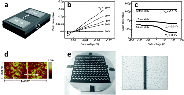 | ||
| Fig. 16 (a) Architecture of a GNRFET. (b) Output characteristics and (c) transfer characteristics of a GNRFET. (d) AFM image of a 9 nm-wide GNR region. (e) Photograph of 144 GNRFETs on a 4-inch wafer with the protective PVK NW not removed. (Reproduced with permission from ref. 145, Copyright 2014, Wiley-VCH Verlag GmbH & Co.) | ||
3. GNRs for electronics and photonic applications
Scalable production techniques potentially enable integration of densely aligned GNRs into circuits as logic, photonic and sensing components. Controlled alignment of GNRs on a large area further permits a variety of applications of GNRs. Numerous papers have reported the development of GNRFETs as discussed above, which will not be covered in the following discussions.3.1. Applications in field-effect transistors
The most important purpose to produce GNRs is to open a bandgap and give them the potential to replace silicon-based FETs in future electronics. Intensive research in recent years has significantly improved the electrical characteristics of GNRFETs, such as their field-effect mobility, on/off current ratio and device density.Field effect mobilities >1000 cm2 V−1 s−1 have been achieved in high-quality GNRs with smooth edges.35,46,76,78,130,131 The on/off current ratio is increased by reducing the GNR width. At RT, e-beam lithographic approaches produce GNRs that have ION/IOFF values >10;34,36 unzipping and NWL approaches could improve the ION/IOFF to >100.12,95 Bilayer GNRs in a vertical electrical field achieved an ION/IOFF of ∼3000.138 So far the highest ION/IOFF values of 105 ≤ ION/IOFF ≤ 107 have been reported in chemically synthesized GNRs by Dai's group.21,56
GNRFET arrays have been massively produced on a wafer scale.65 High-density transistor arrays with 10![[thin space (1/6-em)]](https://www.rsc.org/images/entities/char_2009.gif) 000 top-gated graphene transistors were fabricated on a 0.24 cm2 SiC chip; the density of 40
000 top-gated graphene transistors were fabricated on a 0.24 cm2 SiC chip; the density of 40![[thin space (1/6-em)]](https://www.rsc.org/images/entities/char_2009.gif) 000 cm−2 was a record for graphene electronic devices.76 However, these superior properties are usually reported separately; future development of the research field needs a scalable fabrication technique that can produce GNR arrays with all these superior characteristics at the same time.
000 cm−2 was a record for graphene electronic devices.76 However, these superior properties are usually reported separately; future development of the research field needs a scalable fabrication technique that can produce GNR arrays with all these superior characteristics at the same time.
3.2. Application in logic circuits
The crossbar architecture is a kind of nanoscale array constructed from two orthogonal sets of parallel nanoscale elements (e.g., SiNWs, CNTs, GNRs), in which every crossing point element can be regarded as an electronic device. Gholipour et al. proposed a crossbar-architecture logic circuit based entirely on Schottky-barrier GNRFETs;163 parallel GNRs formed the channel and the metal formed three terminals. Schottky-barrier type graphene nanoribbon field-effect transistors (SB-GNRFETs) were fabricated at the cross points of the GNRs and the metallic gates. The GNR-based crossbar circuits are much superior to conventional CMOS circuits in low-power applications. Habib et al. proposed a graphene nanoribbon tunneling ternary content addressable memory configuration (GNTCAM) based on graphene nanoribbon crossbar (xGNR) structures.164 A crossbar of two vertical GNRs constitutes an xGNR device that has negative differential resistance (NDR) with multiple peak and valley currents (Fig. 17a),165 which can be used as a binary latch or multi-state latch to store information in GNTCAM cell elements. In simulations GNTCAMs were up to 1.82 times denser, up to 1.6 times faster and required as little as 1/9.42 times as much stand-by power consumption than 16 nm CMOS TCAMs. These investigations revealed the great potential of GNRs to realize low-power high-density nanoscale circuits.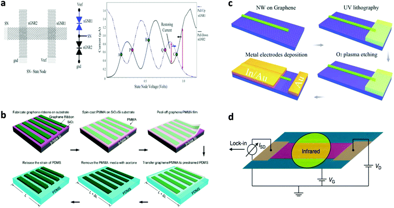 | ||
| Fig. 17 Application of GNRs. (a) Application of GNRs in cross-bar shaped arrays. (Reproduced with permission from ref. 165, Copyright 2014, Elsevier.) (b) Process for fabricating ripple graphene ribbons for use in strain sensors. (Reproduced with permission from ref. 166, Copyright 2011, The American Chemical Society.) (c) Schematic of the fabrication of a GNR/SNW heterojunction LED. (Reproduced with permission from ref. 180, Copyright 2011, The Royal Society of Chemistry). (d) Schematic illustration of an IR detector based on GNRs. (Reproduced with permission from ref. 186, Copyright 2013, Nature Publishing Group.) | ||
3.3. Applications in sensors
3.4. Optoelectronics applications
Another important category of GNR IR photodetectors is based on plasmon resonance by periodic graphene nanoribbon or microribbon arrays with sub-wavelength feature sizes that improve their sensitivity. Ju et al. reported the first investigation of tunable plasmon excitation and light-plasmon coupling at terahertz frequencies in graphene microribbon arrays.185 The authors demonstrated that the plasmon resonance caused by incident light can be easily modulated by electrostatic doping (gate voltage) and the ribbon width; this modulation can control the absorption spectra. The results showed strong terahertz radiation, with >13% absorbance of the plasmon resonance.
Freitag et al. demonstrated the first GNR-based infrared photodetector that exploits the plasmon-light coupling mechanism (Fig. 10d).186 CVD-grown single layer graphene was patterned into GNRs using EBL. GNRs with various widths ranging from 80 nm to 200 nm were evaluated for plasmon resonance. However, the photocurrent must be increased. A sophisticated device structure is required to improve the photoresponse.
4. Conclusions and future prospects
We have reviewed recent progress in the fabrication of GNRs, especially the general processes of methods that show promise for large-scale production of GNRs. The merits and drawbacks of each technique were also discussed. Top-down approaches, such as EBL, NWL, and BCP-template lithography, use aligned nano-patterns as protective masks to cover portions of a graphene sheet, followed by selective removal of unprotected regions to leave nanostructured graphene. Top-down processes are easy and direct ways to achieve scalable fabrication of GNRs. However, the etching process usually entails intense reactions, which produce rough edges with dangling bonds, defects, and various functional groups linked to the edges of GNRs; these rough edges degrade the electrical characteristics. In contrast, bottom-up grown GNRs from nanostructured sites can have high-quality edges and relatively better charge carrier mobility, but the patterning of nanostructured sites still requires top-down approaches, which have limited resolution, and are slow and expensive. Therefore, bottom-up approaches for scalable production of GNRs are inevitably combined with top-down approaches. More efforts are still needed to achieve addressable GNRs on a large area with individually controllable GNR width and atomically smooth edges.Acknowledgements
This work was supported by the Center for Advanced Soft-Electronics funded by the Ministry of Science, ICT and Future Planning, Korea, as Global Frontier Project (Code No. 2014M3A6A5060947).Notes and references
- K. S. Novoselov, A. K. Geim, S. V. Morozov, D. Jiang, Y. Zhang, S. V. Dubonos, I. V. Grigorieva and A. A. Firsov, Science, 2004, 306, 666 CrossRef CAS PubMed.
- F. Schwierz, Nature, 2011, 472, 41 CrossRef CAS PubMed.
- L. Ma, J. Wang and F. Ding, ChemPhysChem, 2013, 14, 47 CrossRef CAS PubMed.
- T.-H. Han, Y. Lee, M.-R. Choi, S.-H. Woo, S.-H. Bae, B. H. Hong, J.-H. Ahn and T.-W. Lee, Nat. Photonics, 2012, 6, 105 CrossRef CAS.
- S.-J. Byun, H. Lim, G.-Y. Shin, T.-H. Han, S. H. Oh, J.-H. Ahn, H. C. Choi and T.-W. Lee, J. Phys. Chem. Lett., 2011, 2, 493 CrossRef CAS.
- S. Bae, H. Kim, Y. Lee, X. Xu, J.-S. Park, Y. Zheng, J. Balakrishnan, T. Lei, H. R. Kim, Y. I. Song, Y.-J. Kim, K. S. Kim, B. Özyilmaz, J.-H. Ahn, B. H. Hong and S. Iijima, Nat. Nanotechnol., 2010, 5, 574 CrossRef CAS PubMed.
- Z. Yan, J. Lin, Z. Peng, Z. Sun, Y. Zhu, L. Li, C. Xiang, E. L. Samuel, C. Kittrell and J. M. Tour, ACS Nano, 2012, 6, 9110 CrossRef CAS PubMed.
- F. Schwierz, Nat. Nanotechnol., 2010, 5, 487 CrossRef CAS PubMed.
- I. Jung, H. Y. Jang and S. Park, Appl. Phys. Lett., 2013, 103, 023105 CrossRef.
- J. Yang, M. Ma, L. Li, Y. Zhang, W. Huang and X. Dong, Nanoscale, 2014, 6, 13301 RSC.
- T. Kato and R. Hatakeyama, Nat. Nanotechnol., 2012, 7, 651 CrossRef CAS PubMed.
- J. Bai, X. Duan and Y. Huang, Nano Lett., 2009, 9, 2083 CrossRef CAS PubMed.
- Y.-W. Son, M. L. Cohen and S. G. Louie, Phys. Rev. Lett., 2006, 97, 216803 CrossRef PubMed.
- L. Yang, C.-H. Park, Y.-W. Son, M. L. Cohen and S. G. Louie, Phys. Rev. Lett., 2007, 99, 186801 CrossRef PubMed.
- Y.-W. Son, M. L. Cohen and S. G. Louie, Nature, 2006, 444, 347 CrossRef CAS PubMed.
- L. Pisani, J. A. Chan, B. Montanari and N. M. Harrison, Phys. Rev. B: Condens. Matter Mater. Phys., 2007, 75, 064418 CrossRef.
- J. Bai, R. Cheng, F. Xiu, L. Liao, M. Wang, A. Shailos, K. L. Wang, Y. Huang and X. Duan, Nat. Nanotechnol., 2010, 5, 655 CrossRef CAS PubMed.
- M. Y. Han, B. Özyilmaz, Y. Zhang and P. Kim, Phys. Rev. Lett., 2007, 98, 206805 CrossRef PubMed.
- M. Evaldsson, I. V. Zozoulenko, H. Xu and T. Heinzel, Phys. Rev. B: Condens. Matter Mater. Phys., 2008, 78, 161407 CrossRef.
- A. Cresti and S. Roche, Phys. Rev. B: Condens. Matter Mater. Phys., 2009, 79, 233404 CrossRef.
- X. Li, X. Wang, L. Zhang, S. Lee and H. Dai, Science, 2008, 319, 1229 CrossRef CAS PubMed.
- E. R. Mucciolo, A. H. Castro Neto and C. H. Lewenkopf, Phys. Rev. B: Condens. Matter Mater. Phys., 2009, 79, 075407 CrossRef.
- D. Querlioz, Y. Apertet, A. Valentin, K. Huet, A. Bournel, S. Galdin-Retailleau and P. Dollfus, Appl. Phys. Lett., 2008, 92, 042108 CrossRef.
- Y. Zhang, Y.-W. Tan, H. L. Stormer and P. Kim, Nature, 2005, 438, 201 CrossRef CAS PubMed.
- K. Wakabayashi, M. Fujita, H. Ajiki and M. Sigrist, Phys. Rev. B: Condens. Matter Mater. Phys., 1999, 59, 8271 CrossRef CAS.
- Y. Miyamoto, K. Nakada and M. Fujita, Phys. Rev. B: Condens. Matter Mater. Phys., 1999, 59, 9858 CrossRef CAS.
- M. Ezawa, Phys. Rev. B: Condens. Matter Mater. Phys., 2006, 73, 045432 CrossRef.
- N. M. R. Peres, A. H. Castro Neto and F. Guinea, Phys. Rev. B: Condens. Matter Mater. Phys., 2006, 73, 195411 CrossRef.
- L. Brey and H. A. Fertig, Phys. Rev. B: Condens. Matter Mater. Phys., 2006, 73, 235411 CrossRef.
- Y. Ouyang, Y. Yoon, J. K. Fodor and J. Guo, Appl. Phys. Lett., 2006, 89, 203107 CrossRef.
- V. Barone, O. Hod and G. E. Scuseria, Nano Lett., 2006, 6, 2748 CrossRef CAS PubMed.
- D. A. Areshkin, D. Gunlycke and C. T. White, Nano Lett., 2007, 7, 204 CrossRef CAS PubMed.
- Z. Chen, Y.-M. Lin, M. J. Rooks and P. Avouris, Physica E, 2007, 40, 228 CrossRef CAS.
- W. S. Hwang, K. Tahy, X. Li, H. Xing, A. C. Seabaugh, C. Y. Sung and D. Jena, Appl. Phys. Lett., 2012, 100, 203107 CrossRef.
- W. S. Hwang, P. Zhao, K. Tahy, L. O. Nyakiti, V. D. Wheeler, R. L. Myers-Ward, C. R. Eddy, D. K. Gaskill, J. A. Robinson, W. Haensch, H. Xing, A. Seabaugh and D. Jena, APL Mater., 2015, 3, 011101 CrossRef.
- J. Sun, T. Iwasaki, M. Muruganathan and H. Mizuta, Appl. Phys. Lett., 2015, 106, 033509 CrossRef.
- V. Sidorkin, E. van Veldhoven, E. van der Drift, P. Alkemade, H. Salemink and D. Maas, J. Vac. Sci. Technol., B: Microelectron. Nanometer Struct.–Process., Meas., Phenom., 2009, 27, L18 CrossRef CAS.
- D. Winston, B. M. Cord, B. Ming, D. C. Bell, W. F. DiNatale, L. A. Stern, A. E. Vladar, M. T. Postek, M. K. Mondol, J. K. W. Yang and K. K. Berggren, J. Vac. Sci. Technol., B: Microelectron. Nanometer Struct.–Process., Meas., Phenom., 2009, 27, 2702 CrossRef CAS.
- W.-D. Li, W. Wu and R. S. Williams, J. Vac. Sci. Technol., B: Nanotechnol. Microelectron.: Mater., Process., Meas., Phenom., 2012, 30, 06F304 Search PubMed.
- M. C. Lemme, D. C. Bell, J. R. Williams, L. A. Stern, B. W. H. Baugher, P. Jarillo-Herrero and C. M. Marcus, ACS Nano, 2009, 3, 2674 CrossRef CAS PubMed.
- D. C. Bell, M. C. Lemme, L. A. Stern, J. R. Williams and C. M. Marcus, Precision Cutting and Patterning of Graphene with Helium Ions, Nanotechnology, 2009, 20, 455301 CrossRef CAS PubMed.
- A. N. Abbas, G. Liu, B. Liu, L. Zhang, H. Liu, D. Ohlberg, W. Wu and C. Zhou, ACS Nano, 2014, 8, 1538 CrossRef CAS PubMed.
- Y. Yinxiao and R. Murali, Impact of Size Effect on Graphene Nanoribbon Transport, IEEE Electron Device Lett., 2010, 31, 237 CrossRef.
- H. Raza and E. C. Kan, Phys. Rev. B: Condens. Matter Mater. Phys., 2008, 77, 245434 CrossRef.
- L. M. Demers, D. S. Ginger, S. J. Park, Z. Li, S. W. Chung and C. A. Mirkin, Science, 2002, 296, 1836 CrossRef CAS PubMed.
- Y.-S. Shin, J. Y. Son, M.-H. Jo, Y.-H. Shin and H. M. Jang, J. Am. Chem. Soc., 2011, 133, 5623 CrossRef CAS PubMed.
- L. Tapaszto, G. Dobrik, P. Lambin and L. P. Biro, Nat. Nanotechnol., 2008, 3, 397 CrossRef CAS PubMed.
- K. V. Emtsev, A. Bostwick, K. Horn, J. Jobst, G. L. Kellogg, L. Ley, J. L. McChesney, T. Ohta, S. A. Reshanov, J. Rohrl, E. Rotenberg, A. K. Schmid, D. Waldmann, H. B. Weber and T. Seyller, Nat. Mater., 2009, 8, 203 CrossRef CAS PubMed.
- W. A. de Heer, C. Berger, X. Wu, P. N. First, E. H. Conrad, X. Li, T. Li, M. Sprinkle, J. Hass, M. L. Sadowski, M. Potemski and G. Martinez, Solid State Commun., 2007, 143, 92 CrossRef CAS.
- X. Li, W. Cai, J. An, S. Kim, J. Nah, D. Yang, R. Piner, A. Velamakanni, I. Jung, E. Tutuc, S. K. Banerjee, L. Colombo and R. S. Ruoff, Science, 2009, 324, 1312 CrossRef CAS PubMed.
- J. Cai, P. Ruffieux, R. Jaafar, M. Bieri, T. Braun, S. Blankenburg, M. Muoth, A. P. Seitsonen, M. Saleh, X. Feng, K. Müllen and R. Fasel, Nature, 2010, 466, 470 CrossRef CAS PubMed.
- S. Linden, D. Zhong, A. Timmer, N. Aghdassi, J. H. Franke, H. Zhang, X. Feng, K. Müllen, H. Fuchs, L. Chi and H. Zacharias, Phys. Rev. Lett., 2012, 108, 216801 CrossRef CAS PubMed.
- H. Sakaguchi, Y. Kawagoe, Y. Hirano, T. Iruka, M. Yano and T. Nakae, Adv. Mater., 2014, 26, 4134 CrossRef CAS PubMed.
- P. Ruffieux, J. Cai, N. C. Plumb, L. Patthey, D. Prezzi, A. Ferretti, E. Molinari, X. Feng, K. Müllen, C. A. Pignedoli and R. Fasel, ACS Nano, 2012, 6, 6930 CrossRef CAS PubMed.
- K. A. Simonov, N. A. Vinogradov, A. S. Vinogradov, A. V. Generalov, E. M. Zagrebina, N. Martensson, A. A. Cafolla, T. Carpy, J. P. Cunniffe and A. B. Preobrajenski, J. Phys. Chem. C, 2014, 118, 12532 CAS.
- X. Wang, Y. Ouyang, X. Li, H. Wang, J. Guo and H. Dai, Phys. Rev. Lett., 2008, 100, 206803 CrossRef PubMed.
- Y.-C. Chen, D. G. de Oteyza, Z. Pedramrazi, C. Chen, F. R. Fischer and M. F. Crommie, ACS Nano, 2013, 7, 6123 CrossRef CAS PubMed.
- T. H. Vo, M. Shekhirev, D. A. Kunkel, M. D. Morton, E. Berglund, L. Kong, P. M. Wilson, P. A. Dowben, A. Enders and A. Sinitski, Nat. Commun., 2014, 5, 3189 Search PubMed.
- P. B. Bennett, Z. Pedramrazi, A. Madani, Y.-C. Chen, D. G. de Oteyza, C. Chen, F. R. Fischer, M. F. Crommie and J. Bokor, Appl. Phys. Lett., 2013, 103, 253114 CrossRef.
- A. Narita, I. A. Verzhbitskiy, W. Frederickx, K. S. Mali, S. A. Jensen, M. R. Hansen, M. Bonn, S. D. Feyter, C. Casiraghi, X. Feng and K. Müllen, ACS Nano, 2014, 8, 11622 CrossRef CAS PubMed.
- O. Endo, M. Nakamura, K. Amemiya and H. Ozaki, Surf. Sci., 2015, 635, 44 CrossRef CAS.
- A. Narita, X. Feng, Y. Hernandez, S. A. Jensen, M. Bonn, H. Yang, I. A. Verzhbitskiy, C. Casiraghi, M. R. Hansen, A. H. R. Koch, G. Fytas, O. Ivasenko, B. Li, K. S. Mali, T. Balandina, S. Mahesh, S. D. Feyter and K. Müllen, Nat. Chem., 2014, 6, 126 CrossRef CAS PubMed.
- Y.-Z. Tan, B. Yang, K. Parvez, A. Narita, S. Osella, D. Beljonne, X. Feng and K. Müllen, Nat. Commun., 2013, 4, 2646 Search PubMed.
- A. N. Abbas, G. Liu, A. Narita, M. Orosco, X. Feng, K. Müllen and C. Zhou, J. Am. Chem. Soc., 2014, 136, 7555 CrossRef CAS PubMed.
- P. Han, K. Akagi, F. F. Canova, H. Mutoh, S. Shiraki, K. Iwaya, P. S. Weiss, N. Asao and T. Hitosugi, ACS Nano, 2014, 8, 9181 CrossRef CAS PubMed.
- H. Zhang, H. Lin, K. Sun, L. Chen, Y. Zagranyarski, N. Aghdassi, S. Duhm, Q. Li, D. Zhong, Y. Li, K. Müllen, H. Fuchs and L. Chi, J. Am. Chem. Soc., 2015, 137, 4022 CrossRef CAS PubMed.
- J. Wu, L. Gherghel, M. D. Watson, J. Li, Z. Wang, C. D. Simpson, U. Kolb and K. Müllen, Macromolecules, 2003, 36, 7082 CrossRef CAS.
- J. Liu, B.-W. Li, Y.-Z. Tan, A. Giannakopoulos, C. Sanchez-Sanchez, D. Beljonne, P. Ruffieux, R. Fasel, X. Feng and K. Müllen, J. Am. Chem. Soc., 2015, 137, 6097 CrossRef CAS PubMed.
- (a) S. Kawai, S. Saito, S. Osumi, S. Yamaguchi, A. S. Foster, P. Spijker and E. Meyer, Nat. Commun., 2015, 6, 8098 CrossRef CAS PubMed; (b) C. Bronner, S. Stremlau, M. Gille, F. Brauße, A. Haase, S. Hecht and P. Tegeder, Angew. Chem., Int. Ed., 2013, 52, 4422 CrossRef CAS PubMed.
- W. J. Yu, S. H. Chae, D. Perello, S. Y. Lee, G. H. Han, M. Yun and Y. H. Lee, ACS Nano, 2010, 4, 5480 CrossRef CAS PubMed.
- C. Berger, Z. Song, T. Li, X. Li, A. Y. Ogbazghi, R. Feng, Z. Dai, A. N. Marchenkov, E. H. Conrad, P. N. First and W. A. de Heer, J. Phys. Chem. B, 2004, 108, 19912 CrossRef CAS.
- C. Berger, Z. Song, X. Li, X. Wu, N. Brown, C. Naud, D. Mayou, T. Li, J. Hass, A. N. Marchenkov, E. H. Conrad, P. N. First and W. A. de Heer, Science, 2006, 312, 1191 CrossRef CAS PubMed.
- J. Hass, W. A. de Heer and E. H. Conrad, J. Phys.: Condens. Matter, 2008, 20, 323202 CrossRef.
- C. Virojanadaraa, R. Yakimovaa, J. R. Osieckia, M. Syväjärvia, R. I. G. Uhrberga, L. I. Johanssona and A. A. Zakharovb, Surf. Sci., 2009, 603, L87 CrossRef.
- J. Robinson, X. Weng, K. Trumbull, R. Cavalero, M. Wetherington, E. Frantz, M. LaBella, Z. Hughes, M. Fanton and D. Snyder, ACS Nano, 2010, 4, 153 CrossRef CAS PubMed.
- M. Sprinkle, M. Ruan, Y. Hu, J. Hankinson, M. Rubio-Roy, B. Zhang, X. Wu, C. Berger and W. A. de Heer, Nat. Nanotechnol., 2010, 5, 727 CrossRef CAS PubMed.
- M. Y. Han, J. C. Brant and P. Kim, Phys. Rev. Lett., 2010, 104, 056801 CrossRef PubMed.
- I. Martin-Fernandez, D. Wang and Y. Zhang, Nano Lett., 2012, 12, 6175 CrossRef CAS PubMed.
- G. Wang, M. Zhang, Y. Zhu, G. Ding, D. Jiang, Q. Guo, S. Liu, X. Xie, P. K. Chu, Z. Di and X. Wang, Sci. Rep., 2013, 3, 2465 Search PubMed.
- J.-H. Lee, E. K. Lee, W.-J. Joo, Y. Jang, B.-S. Kim, J. Y. Lim, S.-H. Choi, S. J. Ahn, J. R. Ahn, M.-H. Park, C.-W. Yang, B. L. Choi, S.-W. Hwang and D. Whang, Science, 2014, 344, 286 CrossRef CAS PubMed.
- R. M. Jacobberger, B. Kiraly, M. Fortin-Deschenes, P. L. Levesque, K. M. McElhinny, G. J. Brady, R. R. Delgado, S. S. Roy, A. Mannix, M. G. Lagally, P. G. Evans, P. Desjardins, R. Martel, M. C. Hersam, N. P. Guisinger and M. S. Arnold, Nat. Commun., 2015, 6, 8006 CrossRef CAS PubMed.
- X. Y. Zhang, H. Li and F. Ding, Adv. Mater., 2014, 26, 5488 CrossRef CAS PubMed.
- Y. T. Lu and H. Metiu, Surf. Sci., 1991, 245, 150 CrossRef CAS.
- R. J. Hamers, U. K. Köhler and J. E. Demuth, Ultramicroscopy, 1989, 31, 10 CrossRef CAS.
- C. Pearson, M. Krueger and E. Ganz, Phys. Rev. Lett., 1996, 76, 2306 CrossRef CAS PubMed.
- J. E. Ayers and S. K. Ghandhi, J. Cryst. Growth, 1988, 89, 371 CrossRef CAS.
- H. Ago, I. Tanaka, Y. Ogawa, R. M. Yunus, M. Tsuji and H. Hibino, ACS Nano, 2013, 7, 10825 CrossRef CAS PubMed.
- A. N. Sokolov, F. L. Yap, N. Liu, K. Kim, L. Ci, O. B. Johnson, H. Wang, M. Vosgueritchian, A. L. Koh, J. Chen, J. Park and Z. Bao, Nat. Commun., 2013, 4, 2402 Search PubMed.
- J. Richter, Metallization of DNA, Physica E, 2003, 16, 157 CrossRef CAS.
- N. Liu, K. Kim, P.-C. Hsu, A. N. Sokolov, F. L. Yap, H. Yuan, Y. Xie, H. Yan, Y. Cui, H. Y. Hwang and Z. Bao, J. Am. Chem. Soc., 2014, 136, 17284 CrossRef CAS PubMed.
- D. V. Kosynkin, A. L. Higginbotham, A. Sinitskii, J. R. Lomeda, A. Dimiev, B. K. Price and J. M. Tour, Nat. Nanotechnol., 2008, 3, 397 CrossRef PubMed.
- F. Cataldo, G. Compagnini, G. Patane, O. Ursini, G. Angelini, P. R. Ribic, G. Margaritondo, A. Cricenti, G. Palleschi and F. Valentini, Carbon, 2010, 48, 2596 CrossRef CAS.
- D. V. Kosynkin, W. Lu, A. Sinitskii, G. Pera, Z. Sun and J. M. Tour, ACS Nano, 2011, 5, 968 CrossRef CAS PubMed.
- Y. Gong, M. Long, G. Liu, S. Gao, C. Zhu, X. Wei, X. Geng, M. Sun, C. Yang, L. Lu and L. Liu, Phys. Rev. B: Condens. Matter Mater. Phys., 2013, 87, 165404 CrossRef.
- L. Jiao, L. Zhang, X. Wang, G. Diankov and H. Dai, Nature, 2009, 458, 877 CrossRef CAS PubMed.
- L. Jiao, X. Wang, G. Diankov, H. Wang and H. Dai, Nat. Nanotechnol., 2010, 5, 321 CrossRef CAS PubMed.
- Z. F. Zhong, H. L. Shen, R. X. Cao, L. Sun, K. P. Li, X. R. Wang and H. F. Ding, J. Appl. Phys., 2013, 113, 174307 CrossRef.
- L. Jiao, L. Zhang, L. Ding, J. Liu, H. Dai, L. Jiao, L. Zhang, L. Ding, J. Liu and H. Dai, Nano Res., 2010, 3, 387 CrossRef CAS.
- A. L. Elias, A. R. Botello-Méndez, D. Meneses-Rodríguez, V. Jehová González, D. Ramírez-González, L. Ci, E. Muñoz-Sandoval, P. M. Ajayan, H. Terrones and M. Terrones, Nano Lett., 2010, 10, 366 CrossRef CAS PubMed.
- W. S. Kim, S. Y. Moon, S. Y. Bang, B. G. Choi, H. Ham, T. Sekino and K. B. Shim, Appl. Phys. Lett., 2009, 95, 083103 CrossRef.
- Y. Maia and A. Eisenberg, Chem. Soc. Rev., 2012, 41, 5969 RSC.
- International Technology Roadmap for Semiconductors, ITRS 2011 Edition (http://www.itrs.net/reports.html), 2011.
- F. S. Bates and G. H. Fredrickson, Annu. Rev. Phys. Chem., 1990, 41, 525 CrossRef CAS PubMed.
- M. Park, C. Harrison, P. M. Chaikin, R. A. Register and D. H. Adamson, Science, 1997, 276, 1401 CrossRef CAS.
- J. Y. Cheng, C. A. Ross, H. I. Smith and E. L. Thomas, Adv. Mater., 2006, 18, 2505 CrossRef CAS.
- J. G. Son, M. Son, K.-J. Moon, B. H. Lee, J.-M. Myoung, M. S. Strano, M.-H. Ham and C. A. Ross, Adv. Mater., 2013, 25, 4723 CrossRef CAS PubMed.
- L. Jiao, L. Xie and H. Dai, Nano Res., 2012, 5, 292 CrossRef CAS.
- G. Liu, Y. Wu, Y.-M. Lin, D. B. Farmer, J. A. Ott, J. Bruley, A. Grill, P. Avouris, D. Pfeiffer, A. A. Balandin and C. Dimitrakopoulos, ACS Nano, 2012, 6, 6786 CrossRef CAS PubMed.
- X. Liang and S. Wi, ACS Nano, 2012, 6, 9700 CrossRef CAS PubMed.
- J. K. W. Yang, Y. S. Jung, J.-B. Chang, R. A. Mickiewicz, A. Alexander-Katz, C. A. Ross and K. K. Berggren, Nat. Nanotechnol., 2010, 5, 256 CrossRef CAS PubMed.
- J. G. Son, A. F. Hannon, K. W. Gotrik, A. Alexander-Katz and C. A. Ross, Adv. Mater., 2011, 23, 634 CrossRef CAS PubMed.
- Y. S. Jung, J. H. Lee, J. Y. Lee and C. A. Ross, Nano Lett., 2010, 10, 3722 CrossRef CAS PubMed.
- X. Wang and H. Dai, Nat. Chem., 2010, 2, 661 CrossRef CAS PubMed.
- X. Wang, S. M. Tabakman and H. Dai, J. Am. Chem. Soc., 2008, 130, 8152 CrossRef CAS PubMed.
- S. M. Lee, Y. H. Lee, Y. G. Hwang, J. R. Hahn and H. Kang, Phys. Rev. Lett., 1999, 82, 217 CrossRef CAS.
- J. R. Hahn, H. Kang, S. M. Lee and Y. H. Lee, J. Phys. Chem. B, 1999, 103, 9944 CrossRef CAS.
- X. Li, H. Wang, J. T. Robinson, H. Sanchez, G. Diankov and H. Dai, J. Am. Chem. Soc., 2009, 131, 15939 CrossRef CAS PubMed.
- G. Xie, Z. Shi, R. Yang, D. Liu, W. Yang, M. Cheng, D. Wang, D. Shi and G. Zhang, Nano Lett., 2012, 12, 4642 CrossRef CAS PubMed.
- V. Abramova, A. S. Slesarev and J. M. Tour, ACS Nano, 2013, 7, 6894 CrossRef CAS PubMed.
- N. S. Safron, M. G. Kim, P. Gopalan and M. S. Arnold, Adv. Mater., 2012, 24, 1041 CrossRef CAS PubMed.
- L. M. Foster, G. Long and M. S. Hunter, J. Am. Ceram. Soc., 1956, 39, 1 CrossRef CAS.
- X. S. Li, W. W. Cai, L. Colombo and R. S. Ruoff, Nano Lett., 2009, 9, 4268 CrossRef CAS PubMed.
- H. Chen, W. Zhu and Z. Zhang, Phys. Rev. Lett., 2010, 104, 186101 CrossRef PubMed.
- X. Duan and C. M. Lieber, Adv. Mater., 2000, 12, 298 CrossRef CAS.
- J. D. Holmes, K. P. Johnston, R. C. Doty and B. A. Korgel, Science, 2000, 287, 1471 CrossRef CAS PubMed.
- Y. Huang and C. M. Lieber, Pure Appl. Chem., 2004, 76, 2051 CrossRef CAS.
- Z. Huo, C.-k. Tsung, W. Huang, X. Zhang and P. Yang, Nano Lett., 2008, 8, 2041 CrossRef CAS PubMed.
- X. Lu, M. S. Yavuz, H.-Y. Tuan, B. A. Korge and Y. Xia, J. Am. Chem. Soc., 2008, 130, 8900 CrossRef CAS PubMed.
- C. Wang, Y. J. Hu, C. M. Lieber and S. H. Sun, J. Am. Chem. Soc., 2008, 130, 8902 CrossRef CAS PubMed.
- C. G. Kang, J. W. Kang, S. K. Lee, S. Y. Lee, C. H. Cho, H. J. Hwang, Y. G. Lee, J. Heo, H.-J. Chung, H. Yang, S. Seo, S.-J. Park, K. Y. Ko, J. Ahn and B. H. Lee, Nanotechnology, 2011, 22, 295201 CrossRef PubMed.
- L. Liao, J. Bai, Y.-C. Lin, Y. Qu, Y. Huang and X. Duan, Adv. Mater., 2010, 22, 1941 CrossRef CAS PubMed.
- C. M. Perkins, B. B. Triplett, P. C. McIntyre, K. C. Saraswat, S. Haukka and M. Tuominen, Appl. Phys. Lett., 2001, 78, 2357 CrossRef CAS.
- Y. C. Yeo, T. J. King and C. M. Hu, J. Appl. Phys., 2002, 92, 7266 CrossRef CAS.
- L. Liao, J. Bai, R. Cheng, Y.-C. Lin, S. Jiang, Y. Huang and X. Duan, Nano Lett., 2010, 10, 1917 CrossRef CAS PubMed.
- M. Cho, J. Park, H. B. Park, C. S. Hwang, J. Jeong and K. S. Hyun, Appl. Phys. Lett., 2002, 81, 334 CrossRef CAS.
- J. W. Bai, X. Zhong, S. Jiang, Y. Huang and X. F. Duan, Nat. Nanotechnol., 2010, 5, 190 CrossRef CAS PubMed.
- I. Meric, M. Y. Han, A. F. Young, B. Özyilmaz, P. Kim and K. L. Shepard, Nat. Nanotechnol., 2008, 3, 654 CrossRef CAS PubMed.
- W. J. Yu and X. Duan, Sci. Rep., 2013, 3, 1248 Search PubMed.
- F. Xia, D. B. Farmer, Y. Lin and P. Avouris, Nano Lett., 2010, 10, 715 CrossRef CAS PubMed.
- B. Sahu, H. Min, A. H. MacDonald and S. K. Banerjee, Phys. Rev. B: Condens. Matter Mater. Phys., 2008, 78, 045404 CrossRef.
- M. P. Lima, A. Fazzio and A. J. R. Silva, Phys. Rev. B: Condens. Matter Mater. Phys., 2009, 79, 153401 CrossRef.
- X. Zhou, C. M. Shade, A. L. Schmucker, K. A. Brown, S. He, F. Boey, J. Ma, H. Zhang and C. A. Mirkin, Nano Lett., 2012, 12, 4734 CrossRef CAS PubMed.
- N. P. Dasgupta, J. Sun, C. Liu, S. Brittman, S. C. Andrews, J. Lim, H. Gao, R. Yan and P. Yang, Adv. Mater., 2014, 26, 2137 CrossRef CAS PubMed.
- M. C. P. Wang and B. D. Gates, Mater. Today, 2009, 12, 34 CrossRef CAS.
- J. Yao, H. Yan and C. M. Lieber, Nat. Mater., 2013, 8, 329 CAS.
- P. A. Smith, C. D. Nordquist, T. N. Jackson, T. S. Mayer, B. R. Martin, J. Mbindyo and T. E. Mallouk, Appl. Phys. Lett., 2000, 77, 1399 CrossRef CAS.
- X. Duan, Y. Huang, Y. Cui, J. Wang and C. M. Lieber, Nature, 2001, 409, 66 CrossRef CAS PubMed.
- C. M. Hangarter and N. V. Myung, Chem. Mater., 2005, 17, 1320 CrossRef CAS.
- Y. Huang, X. Duan, Q. Wei and C. M. Lieber, Science, 2001, 291, 630 CrossRef CAS PubMed.
- X. Duan, C. Niu, V. Sahi, J. Chen, J. Wallace Parce, S. Empedocles and J. L. Goldman, Nature, 2003, 425, 274 CrossRef CAS PubMed.
- G. Yu, A. Cao and C. M. Lieber, Nat. Nanotechnol., 2007, 2, 372 CrossRef CAS PubMed.
- A. Tao, F. Kim, C. Hess, J. Goldberger, R. He, Y. Sun, Y. Xia and P. Yang, Nano Lett., 2003, 3, 1229 CrossRef CAS.
- Z. Fan, J. C. Ho, T. Takahashi, R. Yerushalmi, K. Takei, A. C. Ford, Y.-L. Chueh and A. Javey, Adv. Mater., 2009, 21, 3730 CrossRef CAS.
- K. Takei, T. Takahashi, J. C. Ho, H. Ko, A. G. Gillies, P. W. Leu, R. S. Fearing and A. Javey, Nat. Mater., 2010, 9, 821 CrossRef CAS PubMed.
- Q. Cao, H.-S. Kim, N. Pimparkar, J. P. Kulkarni, C. Wang, M. Shim, K. Roy, M. A. Alam and J. A. Rogers, Nature, 2008, 454, 495 CrossRef CAS PubMed.
- J. K. N. Mbindyo, B. D. Reiss, B. R. Martin, C. D. Keating, M. J. Natan and T. E. Mallouk, Adv. Mater., 2001, 13, 249 CrossRef CAS.
- M. Chen, L. Guo, R. Ravi and P. C. Searson, J. Phys. Chem. B, 2006, 110, 211 CrossRef CAS PubMed.
- J. Chai, D. Wang, X. Fan and J. M. Buriak, Nat. Nanotechnol., 2007, 2, 500 CrossRef PubMed.
- S.-Y. Min, T.-S. Kim, B. J. Kim, H. Cho, Y.-Y. Noh, H. Yang, J. H. Cho and T.-W. Lee, Nat. Commun., 2013, 4, 1773 CrossRef PubMed.
- W. Xu, H.-K. Seo, S.-Y. Min, H. Cho, T.-S. Lim, C.-y. Oh, Y. Lee and T.-W. Lee, Adv. Mater., 2014, 26, 3459 CrossRef CAS PubMed.
- W. Xu, T.-S. Lim, H.-K. Seo, S.-Y. Min, H. Cho, M.-H. Park, Y.-H. Kim and T.-W. Lee, Small, 2014, 10, 1999 CrossRef CAS PubMed.
- W. Xu, L. Wang, Y. Liu, S. Thomas, H.-K. Seo, K.-I. Kim, K. S. Kim and T.-W. Lee, Adv. Mater., 2015, 27, 1619 CrossRef CAS PubMed.
- M. Gholipour and N. Masoumi, Microelectron. J., 2014, 45, 1533 CrossRef CAS.
- K. M. M. Habib and R. K. Lake, Phys. Rev. B: Condens. Matter Mater. Phys., 2012, 86, 045418 CrossRef.
- S. Khasanvis, M. Rahman and C. A. Moritz, J. Parallel Distrib. Comput., 2014, 74, 2497 CrossRef.
- Y. Wang, R. Yang, Z. W. Shi, L. C. Zhang, D. X. Shi, E. Wang and G. Y. Zhang, ACS Nano, 2011, 5, 3645 CrossRef CAS PubMed.
- R. K. Joshi, H. Gomez, F. Alvi and A. Kumar, J. Phys. Chem. C, 2010, 114, 6610 CAS.
- J. L. Johnson, A. Behnam, S. J. Pearton and A. Ural, Adv. Mater., 2010, 22, 4877 CrossRef CAS PubMed.
- J. L. Johnson, A. Behnam, Y. An, S. J. Pearton and A. Ural, J. Appl. Phys., 2011, 109, 124301 CrossRef.
- A. Martína, J. H. Ferrerb, M. T. Martínezb and A. Escarpaa, Electrochim. Acta, 2015, 172, 2 CrossRef.
- L. Shang, F. Q. Zhao and B. Z. Zeng, Electrochim. Acta, 2015, 168, 330 CrossRef CAS.
- X. B. Tan, H. J. Chuang, M. W. Lin, Z. X. Zhou and M. M. Cheng, J. Phys. Chem. C, 2013, 117, 27155 CAS.
- S. Wu, X. Q. Lan, F. F. Huang, Z. Z. Luo, H. X. Ju, C. G. Meng and C. Y. Duan, Biosens. Bioelectron., 2012, 32, 293 CrossRef CAS PubMed.
- E. Asadian, S. Shahrokhian, A. I. Zad and E. Jokar, Sens. Actuators, B, 2014, 196, 582 CrossRef CAS.
- A. Martín, P. Batalla, J. Hernández-Ferrer, M. T. Martínez and A. Escarpa, Biosens. Bioelectron., 2015, 68, 163 CrossRef PubMed.
- N. S. Ismail, Q. H. Le, H. Yoshikawa, M. Saito and E. Tamiya, Electrochim. Acta, 2014, 146, 98 CrossRef CAS.
- F. Traversi, C. Raillon, S. M. Benameur, K. Liu, S. Khlybov, M. Tosun, D. Krasnozhon, A. Kis and A. Radenovic, Nat. Nanotechnol., 2013, 8, 939 CrossRef CAS PubMed.
- X. F. Shen, Y. Cui, Y. H. Pang and H. Qian, Electrochim. Acta, 2012, 59, 91 CrossRef CAS.
- A. Martin, J. Hernandez-Ferrer, L. Vazquez, M. Martinezb and A. Escarpa, RSC Adv., 2014, 4, 132 RSC.
- Y. Ye, L. Gan, L. Dai, H. Meng, F. Wei, Y. Dai, Z. J. Shi, B. Yu, X. F. Guo and G. G. Qin, J. Mater. Chem., 2011, 21, 11760 RSC.
- B. Chitara, L. S. Panchakarla, S. B. Krupanidhi and C. N. R. Rao, Adv. Mater., 2011, 23, 5419 CrossRef CAS PubMed.
- E. U. Stützel, T. Dufaux, A. Sagar, S. Rauschenbach, K. Balasubramanian, M. Burghard and K. Kern, Appl. Phys. Lett., 2013, 102, 043106 CrossRef.
- X. Wang, L. Zhi and K. Müllen, Nano Lett., 2008, 8, 323 CrossRef CAS PubMed.
- J. Wu, H. A. Becerril, Z. Bao, Z. Liu, Y. Chen and P. Peumans, Appl. Phys. Lett., 2008, 92, 263302 CrossRef.
- L. Ju, B. Geng, J. Horng, C. Girit, M. Martin, Z. Hao, H. A. Bechtel, X. Liang, A. Zettl, Y. R. Shen and F. Wang, Nat. Nanotechnol., 2011, 6, 630 CrossRef CAS PubMed.
- M. Freitag, T. Low, W. Zhu, H. Yan, F. Xia and P. Avouris, Nat. Commun., 2013, 4, 1951 Search PubMed.
| This journal is © The Royal Society of Chemistry 2016 |


