 Open Access Article
 This Open Access Article is licensed under a Creative Commons Attribution-Non Commercial 3.0 Unported Licence
Template-assisted colloidal self-assembly of macroscopic magnetic metasurfaces†
Martin
Mayer
ac,
Moritz
Tebbe
b,
Christian
Kuttner
ac,
Max J.
Schnepf
a,
Tobias A. F.
König
*acd and
Andreas
Fery
*ace
aLeibniz-Institut für Polymerforschung Dresden e.V., Institute of Physical Chemistry and Polymer Physics, Hohe Str. 6, 01069 Dresden, Germany. E-mail: koenig@ipfdd.de; fery@ipfdd.de
bDepartment of Physical Chemistry II, University of Bayreuth, Universitätsstr. 30, 95440 Bayreuth, Germany
cCluster of Excellence Centre for Advancing Electronics Dresden (CFAED), Technische Universität Dresden, 01062 Dresden, Germany
dTechnische Universität Dresden, Fakultät Mathematik und Naturwissenschaften, 01062 Dresden, Germany
eDepartment of Physical Chemistry of Polymeric Materials, Technische Universität Dresden, Hohe Str. 6, 01069 Dresden, Germany
First published on 22nd February 2016
Abstract
We demonstrate a template-assisted colloidal self-assembly approach for magnetic metasurfaces on macroscopic areas. The choice of anisotropic colloidal particle geometry, assembly pattern and metallic film is based on rational design criteria, taking advantage of mirror-charge effects for gold nanorods placed on gold film. Monodisperse gold nanorods prepared utilizing wet-chemistry are arranged with high precision on wrinkled templates to form linear array-type assemblies and subsequently transferred to a thin gold film. Due to the obtained particle-to-film distance of 1.1 nm, the plasmonic mode of the nanorod is able to couple efficiently with the supporting metallic film, giving rise to a magnetic mode in the visible spectrum (721 nm). Conventional UV-vis-NIR measurements in close correlation with electromagnetic simulations provide evidence for the presence of a magnetic resonance on the macroscopic area. The herein presented scalable lithography-free fabrication process paves the road towards colloidal functional metasurfaces with an optical response in the effective magnetic permeability.
Introduction
Recent interest in designing metamaterials focuses on the step from 3D bulk materials to 2D metasurfaces, which feature similar optical features.1–6 Metasurfaces are optical functional interfaces based on regular patterns of subwavelength repeating metaatoms (unit cells). The controlled arrangement of metaatoms allows the engineering of novel optical devices based on controlled reflectance,7,8 efficient energy transport and wave guiding,9,10 as well as perfect lensing11 and optical magnetism.12 For many of these applications, the main challenge is the control of the magnetic resonances in the visible optical range. The lack of magnetic response in natural optical materials13 was first overcome by artificial magnetic resonances obtained for split-ring resonators in the micro-wave regime.3 However for split-ring resonators, the limited scalability and saturation effects14 deny their application in the visible optical range.Consequently, the fabrication of nanostructures with magnetic resonances remains a challenge especially on macroscopic areas. The design of such magnetic metasurfaces needs to be rationally linked to scalable fabrication techniques of hierarchical assemblies in quasi 2D-resonators.5 The incident electric-field component induces oscillating charges within the resonators and, hence, gives rise to an effective magnetic moment; this excitation is commonly referred to as a magnetic resonance.15–17 To achieve these effects, metasurfaces have to be built with nanometre precision.18,19 Common fabrication techniques rely on lithographic methods, like e-beam lithography or ion-beam milling, which have several drawbacks, such as losses due to polycrystallinity and lack in resolution and scalability.20–24 The colloidal bottom-up assembly approach, which exploits the advantages of noble metal nanoparticles synthesized using wet-chemistry (e.g., single-crystallinity, scalability), can provide alternatives to lithographic top-down techniques.25–27 However, those approaches often rely on random particle deposition, which strongly limits the complexity of the prepared unit cells and the homogeneity of the obtained metasurfaces.28–30 To boost the complexity of the fabricated metasurfaces, plasmonic nanoparticles are coupled to metallic films to form mirror charges in the emerging cavities.8,10,31–33 Template-assisted convective self-assembly allows the design of unit cells with high complexity and in a large variety by surface-alignment of nanoparticles in well-defined orientations. Such assemblies are only limited by the scalability and spatial resolution of the directing template.34–36
In this work, we use a lithography-free colloidal bottom-up approach to fabricate a macroscopic magnetic metasurface. Plasmonic nanoparticles in close contact with a metallic film induce electric current loops due to mirrored charges at the substrate, which give rise to a magnetic mode. We provide theoretical explanations for the experimentally observed magnetic mode through electromagnetic modelling and conventional UV-vis-NIR spectroscopy. Anisotropic nanoparticles are used, due to the following reasons: the short axis of the nanorods is used for magnetic mode excitation and their long axes provide control over their orientation in template-assisted self-assembly. For the building block, we used tailored wet-chemical synthesis to obtain monodisperse, gold nanorods with defined crystalline facets (flat faces). Furthermore, due to a defined spacer material we obtain a reliable particle-to-film distance. Using colloidal self-assembly, we were able to fabricate a macroscopic magnetic metasurface, which shows a clear signature of an effective magnetic permeability in the visible wavelength range. With this colloidal approach, we aim for a reliable method to make the unique manipulation of light on the macroscale possible.
Results and discussion
Design of the metasurface unit cell
One of the central prerequisites for obtaining a magnetic resonance is the induction of a circular oscillating current flow within the unit cell. This can be achieved by the efficient coupling of the surface plasmon with the electric component of the incident light.15,37 Isolated nanoparticles in solution inherently exhibit electric modes in the form of localized surface plasmon resonances, as indicated for an exemplary dipolar-isolated mode (EM) by its surface charges (Fig. 1A, electric mode).38 Breaking the symmetry is achieved by coupling a plasmonic nanoparticle to a substrate. The emerging modes depend strongly on the substrate material, nanoparticle geometry and particle-to-film distance. In contrast to nanospheres, nanoparticles with flat faces are advantageous because of their larger contact area with the substrate, which results in narrow resonances and enhanced excitation.39 The interaction of a nanoparticle with a dielectric substrate results in hybridized modes.40 On the contrary, when a particle is coupled to a metallic substrate, the dipolar mode induces a mirror charge pattern at the surface of the metallic film (Fig. 1A, magnetic mode).41–43 These mirror charges may induce an electric current loop (current density J), as calculated by electromagnetic simulations. According to Ampère's circuital law, a magnetic moment is excited.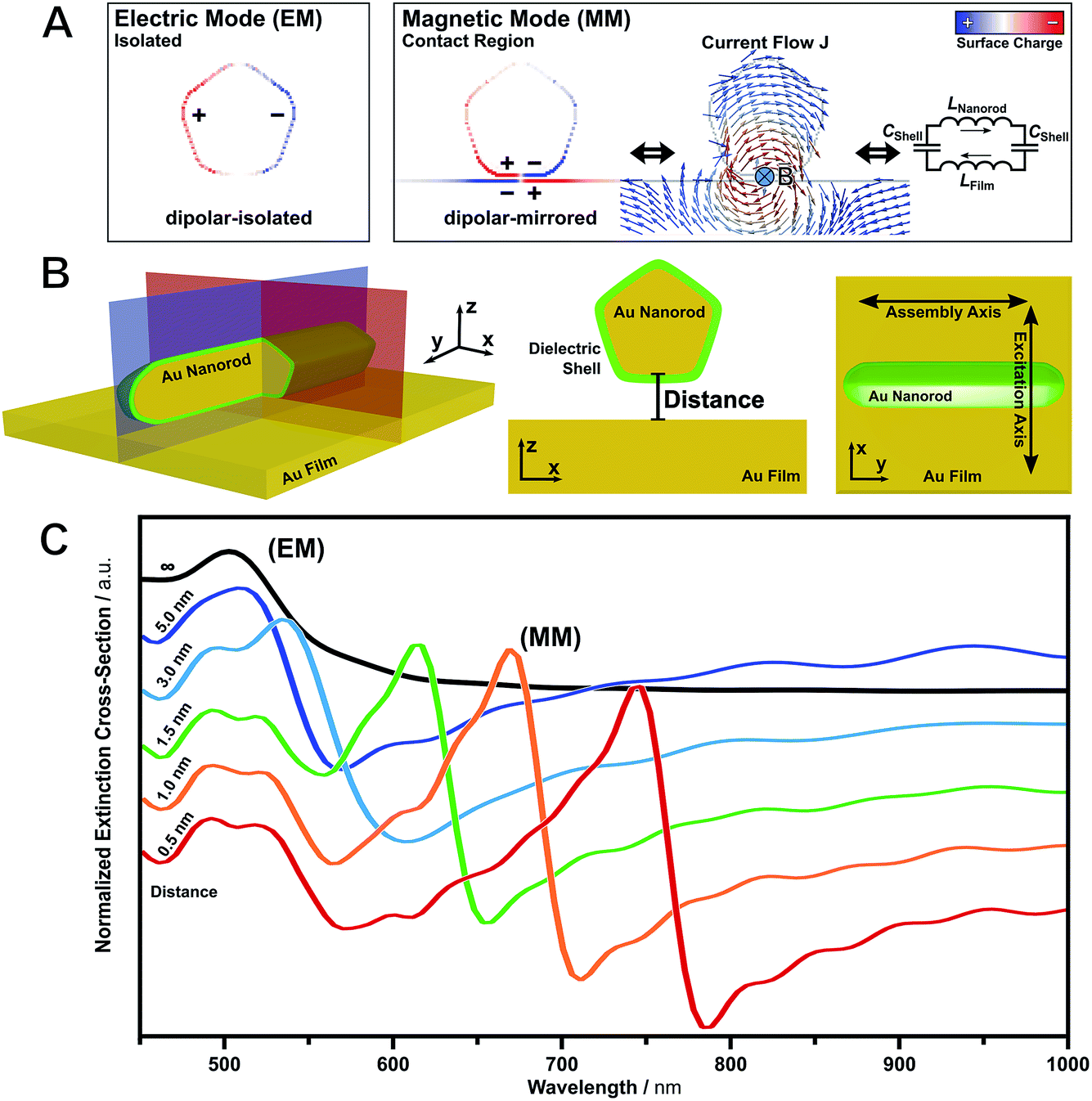 | ||
| Fig. 1 Evolution of magnetic modes – from electric to magnetic resonance through metallic film-coupled plasmonic nanoparticles. (A) Surface charge pattern of an electric mode (EM), magnetic mode (MM), characteristic electric current loop (flow J) and representative inductor–capacitor (LC) model for one unit cell. (B) Schematic representation of the unit cell: gold nanorods (160 nm × 30 nm) on a 40 nm thin gold film. The short axis of the nanorod is used for the excitation by linear polarized light (transversal mode) and the long axis is used for directing the assembly process. (C) Calculated extinction cross-section at different particle-to-film distances, normalized against the bare gold film. | ||
Recently, Wang et al. have numerically demonstrated that magnetic modes can be represented by an inductor–capacitor (LC) model (Fig. 1A).8 For film-coupled nanoparticles, the metal components act as inductors L, whereas the dielectric insulator acts as a capacitor C. Thus, the resonance wavelengths λ(MM) of the dipolar-mirrored mode (MM) can be expressed using the following equation:
 | (1) |
However, an analytical calculation by means of eqn (1) is not straightforward, since the inductance and the capacitance depend on the curvature and geometry of the nanoparticle. Nevertheless, the model provides an intuitive description of the counter-oscillating currents in the unit cell. Consequently, a metasurface can be designed based on film-coupled nanoparticles.
We decided to design our magnetic metasurface based on film-coupled nanorods utilizing their short axes for magnetic mode excitation (transversal mode) and their long axes for providing orientational order upon self-assembly (Fig. 1B). The transversal magnetic mode is excited if the electric field component is planar with the cross-section of the unit cell (xz-plane, red). In contrast, the longitudinal magnetic mode, which could be excited with the electric field parallel to the long axis (yz-plane, blue), is significantly shifted outside the frequency range of visible light and will not be discussed further. Fig. 1B shows a schematic depiction of the proposed metasurface unit cell consisting of a nanoparticle as a building block positioned over a metallic film. The capping agent of the nanoparticle serves as a thin dielectric shell. For observation of the magnetic mode with conventional spectroscopy methods, an array of well-aligned anisotropic nanoparticles is required. For colloidal metasurface design, 1D periodic arrangements are ideal as they provide collective alignment of nanorods along their long axes. At the same time, a distance of at least five nanorod radii between the lines will suppress grating effects.44 Tip-to-tip coupling within nanorod lines is decoupled from transversal excitation and does not interfere with the induction of the magnetic resonance.
Comprehensive numerical simulations of this unit cell clearly reveal that the spectral position of the magnetic mode can be tailored by tuning the following four parameters: (I) the dimensions and shape of the plasmonic nanoparticle; (II) the refractive index of the dielectric spacer (e.g., capping agent); (III) the material of the plasmonic nanoparticle and (IV) the coupling distance between the nanoparticle surface and the substrate. These four parameters need to be precisely balanced to provide a strong magnetic resonance within the visible spectrum. However, tuning of the first three parameters is limited by: (I) the dimension of the nanorods (approximately 30 nm in width);45 (II) the index of refraction of the spacer material (roughly from 1.4 to 1.5 for polymeric materials);46 and (III) the limited choice in plasmonic metals. Silver as well as gold both possess plasmonic properties in the optical range. However, even though silver features lower damping, offering narrower line-widths and higher intensities,47,48 it is vulnerable against sulfidation and oxidation in the air.49 Consequently, we choose gold in the present study. In contrast, the particle-to-film separation can be controlled by the capping agent and an additional spacer layer at the substrate, e.g., by layer-by-layer techniques.50 In combination, the cavity size can be tailored with nanometre precision. Taking the limited range of optimization of the nanorod morphology and the index of refraction of the building blocks into account, we will focus on the size of the nanoparticle-film cavity in order to further optimise the metasurface design.
Fig. 1C shows the extinction cross-section σext of a nanorod at varying distances from a metallic film. The extinction spectra were normalized against the transmission (T) of the bare gold film (σext = −log![[thin space (1/6-em)]](https://www.rsc.org/images/entities/char_2009.gif) 1/T, transparent for green light only). Owing to the transmission characteristics of gold, the extinction cross-sections show a pseudo-resonance below the interband gap of gold (<512 nm) and a pronounced increase in extinction towards lower energy. The isolated particle monomer, i.e. at infinite separation, shows a single plasmonic resonance (electric mode, EM). This transversal excitation corresponds to the electric mode as discussed above. Approaching the surface, the dipolar electric mode is converted to a magnetic dipolar-mirrored mode (magnetic mode, MM) and a higher-order magnetic mode. This quadrupolar-mirrored mode is further discussed in the ESI, Fig. S1.† The magnetic resonance shifts towards lower energy in comparison to the isolated electric mode. This characteristic red-shift is also known as a plasmon ruler.51 The spectral position of the magnetic mode is particularly sensitive to distance changes even in the angstrom range. Thus, the resonance frequency may be tuned over the entire optical range. To avoid effects like quantum tunnelling, a minimum distance of 0.4 nm should be sustained.52,53 These separations lie within the range of conventional capping agents.54 Next, we will address the fabrication of suitable nanoparticles as building blocks.
1/T, transparent for green light only). Owing to the transmission characteristics of gold, the extinction cross-sections show a pseudo-resonance below the interband gap of gold (<512 nm) and a pronounced increase in extinction towards lower energy. The isolated particle monomer, i.e. at infinite separation, shows a single plasmonic resonance (electric mode, EM). This transversal excitation corresponds to the electric mode as discussed above. Approaching the surface, the dipolar electric mode is converted to a magnetic dipolar-mirrored mode (magnetic mode, MM) and a higher-order magnetic mode. This quadrupolar-mirrored mode is further discussed in the ESI, Fig. S1.† The magnetic resonance shifts towards lower energy in comparison to the isolated electric mode. This characteristic red-shift is also known as a plasmon ruler.51 The spectral position of the magnetic mode is particularly sensitive to distance changes even in the angstrom range. Thus, the resonance frequency may be tuned over the entire optical range. To avoid effects like quantum tunnelling, a minimum distance of 0.4 nm should be sustained.52,53 These separations lie within the range of conventional capping agents.54 Next, we will address the fabrication of suitable nanoparticles as building blocks.
Synthesis of well-defined building blocks
Gold nanorods possess intrinsic anisotropy in both their geometrical and optical properties. Thus, nanorods, as well as their top-down lithographic equivalents, are common building blocks in metamaterial fabrication, e.g., as in the well-known double-bar setup.15,18,55 The fabrication of hierarchical unit cells of high precision requires building blocks of well-defined size and shape (Fig. 2). High structural integrity is critical for the performance of the final system, because disorder and polydispersity in size and shape yield additional undesired resonance broadening. By using wet-chemical bottom-up synthesis, a variety of monodisperse building blocks is accessible. In particular, the control over nanoparticle size, shape, and crystallinity allows for tailored morphological and optical properties.56,57 The penta-twinned nanorods used were prepared by seed-mediated growth based on a modified protocol by Pérez-Juste et al.45,58 combined with a supplemental purification step employing depletion forces.59,60 | ||
| Fig. 2 Gold nanorods in solution – nature of the electric modes. (A) TEM image of the purified gold nanorods with mean dimensions of 161.0 ± 14.8 nm in length and 30.2 ± 3.7 nm in width. (B) Experimental (red) and simulated (black) extinction spectra. The gold nanorods exhibit three electric plasmon resonances, which can be attributed to dipolar transversal (TEM, 512 nm), dipolar longitudinal (Ld, 1087 nm) and quadrupolar longitudinal (Lq, 680 nm) modes. The corresponding surface charges of the dipolar excitations are shown as insets. | ||
With this method, penta-twinned gold nanorods can be produced which exhibit larger thicknesses and higher aspect ratios compared to the more commonly used single-crystalline gold nanorods.61 Additionally, their pentagonal cross-section and their flat sides are beneficial for substrate-supported effects due to the increased interaction areas. However, owing to the use of twinned seeds only 20% of the resulting nanoparticles are nanorods with the majority being spherical and 2D by-products. These by-products need to be removed as they strongly impede the bottom-up self-assembly of hierarchical unit cells. Consequently, a supplemental purification step is required to yield narrow distributions. Efficient separation can be achieved by exploiting depletion forces with additional surfactants acting as depletants, as published recently.59,60 Here, the effective physical parameter is the interaction area and, thus, the morphology of the nanoparticles in solution. To avoid time-consuming screening for an adequate depletant (i.e., surfactant) concentration, we measured a calibration curve which allows the purification of penta-twinned gold nanorods depending on their longitudinal localized surface plasmon resonance (see ESI Fig. S2†). This purification protocol enables almost quantitative removal of spherical by-products and other morphologies. A second purification step is performed to remove longer and thinner nanorods to selectively tune and enhance the size-distribution. Fig. 2 shows a TEM image (A) and extinction spectra (B) of the synthesized and purified nanorod sample. The nanorods exhibited mean dimensions of 161.0 ± 14.8 nm in length and 30.2 ± 3.7 nm in width (for as-synthesized TEM images, UV-vis spectra and histograms of the size distribution, see ESI Fig. S2†). Consequently, the herein presented 3-step protocol is an ideal means to precisely tailor the aspect ratio of nanorods. The dipolar electric characters of the transversal (TEM) and the predominant longitudinal plasmon resonance (Ld) are depicted by their surface charges in Fig. 2 (insets).
For the successful template-assisted convective assembly the wetting behaviour of the nanorods is critical. As shown recently by our group, surface chemistry providing enhanced wettability can be adjusted using surface functionalisation with a hydrophilic protein shell.21,55 Consequently, concentrated highly stable solutions of gold nanorods with bovine serum albumin (BSA)21 as dielectric shells were obtained for subsequent assembly. In the dry state, the BSA layer exhibits a shell thickness below 2 nm as we have shown in previous work. Consequently, these nanoparticles match the requirements for reliable template-assisted colloidal self-assembly. In the following, we focus on the self-assembly of the nanorods into array-type structures.
Fabrication of film-coupled nanorod arrays as magnetic unit cells
Controlled colloidal self-assembly of the nanoscale building blocks into the proposed magnetic unit cell is an important step towards a macroscopic magnetic metasurface (Fig. 3). Recently, we demonstrated the precise alignment of nanorods into well-defined 1D particle lines using template-assisted convective self-assembly employing wrinkled elastomeric substrates.55 In the first fabrication step, the nanorods are assembled in the form of tip-to-tip arrangements within the periodic structure of the wrinkle. In order to achieve periodic macroscopic alignment in single particle lines the templates need to be homogeneous on square-centimetre scales. The dimensions of its features are crucial and need to precisely match the nanorod dimensions (i.e., width). The employed wrinkled templates are fabricated by plasma treatment of a macroscopic uniaxially stretched polydimethylsiloxane (PDMS) elastomer. The plasma treatment introduces a thin oxidized film at the surface. Upon strain release, periodic wrinkles are formed due to the mechanical mismatch between the substrate and the thin film.62 The template periodicity is critical for controlling the period of the alignment. To avoid any grating effects the periodicity was chosen to be sufficiently large (see discussion above for more details). Thus, periodicity and amplitude were tuned to values of 210 nm and 40 nm, respectively.62 Subsequently, the amplitude was reduced to 20 nm by additional plasma post-treatment without altering the periodicity to match the dimensions of the employed gold nanorods.55 At the same time, the surface is hydrophilized sufficiently to enable subsequent nanoparticle assembly from aqueous solution (see plasma post-treatment calibration in the ESI Fig. S3†). | ||
| Fig. 3 Macroscopic template-assisted self-assembly using mechanical instabilities. (A) Schematic template-assisted self-assembly process by dip coating the wrinkled templates in a highly concentrated gold nanorod solution. (B) AFM image of the self-assembled array of gold nanorods in the wrinkle template. (C) Schematic transfer process using wet-contact printing and subsequent lift-off of the emptied template. (D) SEM image of the assembled structures transferred to a smooth gold film and photographs of the macroscopic substrate in reflection and transmission (upper and lower inset, respectively). | ||
Nanorod assembly into single particle lines was achieved by dip coating. The unidirectional laminar flow promotes the orientation of the anisotropic particles along the major (long) axis. Fig. 3A displays schematically the self-assembly process. Macroscopic templates are withdrawn from a highly concentrated nanoparticle solution (2 mg mL−1). During withdrawal, the nanorods are aligned into the channels by capillary forces within the confined meniscus (see Fig. 3B). Due to the confinement of the wrinkle structure, we are able to align the building blocks for a further transfer step.
In the second fabrication step, we use the wet-contact print method to transfer the pre-aligned anisotropic nanorods onto the gold film. The building blocks were transferred to a hydrophilized gold film while maintaining their orientational order. Utilizing template stripping, a surface roughness of the gold film below 1 nm was achieved. Consequently, a uniform contact between the nanorods and the supporting gold film is provided. Quantitative transfer can be achieved by wet-transfer printing of the prefilled templates and subsequent lift-off of the emptied template as schematically depicted in Fig. 3C. Contrary to the transfer to other surface materials,55 an additional adhesion promoter is not required. The combination of van der Waals interactions between the gold nanoparticles and gold film and the gold-selective binding groups of the protein shell (e.g., amine, thiol) is sufficient to guarantee a complete transfer. Thus, sufficient particle–substrate spacing is given solely by the thickness of the dried shell of the stabilizing agent at the nanorod surface. The successful transfer covers an area of 5 mm × 5 mm as evidenced by SEM micrographs and macroscopic photographs (see Fig. 3D).
The quality of the assembled structures was evaluated using statistical analysis of the position and orientation of the particles with high magnification SEM images (360 individual nanorods, for further information see ESI Fig. S4†). The tip-to-tip particle spacing was determined to be 15.6 ± 5.8 nm within the lines and 209 ± 6 nm between neighbouring lines, in-line with the template periodicity. The high structural precision of the assembly was evidenced by the averaged deviation θ to the principle alignment direction 〈σθ〉 being only 2.69° corresponding to a 2D-order parameter 〈S2D〉 of 0.99 (〈S2D〉 = 〈2cos2(θ) − 1〉). This large-yield and scalable method enabled us to fabricate a metasurface array of film-coupled nanorods on the macroscale. The following section will elucidate its optical characteristics.
Optical characterisation of film-coupled nanorod arrays
The optical properties of the macroscopic assemblies were investigated using conventional far-field UV-vis-NIR measurements. Since the magnetic resonance is dominated by absorption, spectroscopy was performed in the transmission geometry.63 In order to allow spectroscopy in transmission, the thickness of the gold film was set to 34 nm (Fig. 3D, insets). In the visible wavelength range, the magnetic mode is excited only if the polarized light is in plane with the cross-section of the nanorod (transversal mode). Experimentally, this excitation was performed on a spot size of 4 mm × 4 mm using polarized spectroscopy measurements. Fig. 4 shows the extinction spectrum normalized against the bare gold film. | ||
| Fig. 4 Macroscopic magnetic metasurfaces. (A) SEM image of the template-assisted self-assembled array of film-coupled nanorods. (B) Simulated magnetic (|H|2/|H0|2, coloured scale range from 1 to 4) and electric field intensity (|E|2/|E0|2, coloured scale range from 1 to 100) of the unit cell. (C) Experimentally observed UV-vis-NIR (red) and modelled (blue) extinction spectra of the metasurface. Modelled transversal extinction spectrum of an isolated nanorod (black, not to scale). (D) Modelled extinction spectra of the magnetic mode at various particle-to-film distances (0.9 nm to 1.3 nm) and the averaged result. | ||
Experimentally we observe the clear spectral signature of a magnetic mode (MM) with its peak intensity at 675 nm and point of inflexion at 721 nm (Fig. 4C). In addition, the quadrupolar-mirrored mode at 556 nm is present. The experimental observation is in excellent agreement with the modelling results of a film-coupled nanorod array (blue). The extinction cross-section of an isolated nanorod in air (transversal excitation, black) indicates the position of the initial electric mode (EM). From the position of the magnetic mode (MM), a mean particle-to-film distance of 1.1 nm was extracted. This distance is still above the quantum tunnelling limit of 0.4 nm.53 The small deviation between the experiment and the model can be attributed to the high sensitivity towards particle-to-film distances. This influence is determined in Fig. 4D for various distances from 0.9 nm to 1.3 nm. This further emphasises the high sensitivity of the mode towards distance variations. Consequently, macroscopic magnetic substrates may be tuned over the entire visible spectrum.
Effective magnetic properties of the metasurface
To quantify the magnitude of the magnetic response of the metasurface, we modelled the effective optical properties using the S-parameter retrieval method established by D. R. Smith et al.64 This method is in close analogy to the inductor–capacitor (LC) model (see eqn (1) and Fig. 5A). For this purpose, the anisotropic optical response must be calculated in the forward and backward direction (S-parameters). The model was built based on identical parameters (i.e., nanorod dimensions, shell and film thickness, particle-to-film distance) to those described above. | ||
| Fig. 5 Effective magnetic properties of film-coupled nanorods. (A) Schematic representation of the S-parameter retrieval method and analogy to the inductor–capacitor (LC) model. The unit cell is treated as an effective medium, since only the S-parameters are evaluated in the forward and backward direction. (B) Calculated magnetic permeability for the film-coupled nanorod revealing the presence of a magnetic resonance and related magnetic field (inset). | ||
Before we can understand the effective magnetic permeability of the unit cell, we will discuss the optical properties of the following building blocks: (I) the bare gold film and (II) the gold nanorod monomer (ESI Fig. S5†). These steps are important to prove the stability of the S-parameter method in this frequency range. (I) The calculated effective electric permittivity of the bare gold film (40 nm thickness) agrees well with literature values (see Methods part). (II) The optical properties of the individual gold nanorod monomer are of particular interest for colloidal optical metamaterial design, because the bulk real part of the permittivity of gold is always negative. Once the metallic particle is surrounded by dielectric medium, the real part of the permittivity turns positive, which is in good agreement with the observations described in literature.65
Adding a film to the nanorod will result in a clear response in the complex magnetic permeability (Fig. 5B). The imaginary part of the permeability reveals the energetic location of the magnetic resonance through its characteristic peak at the point of inflexion of the extinction, whereas the real part shows the typical slope at the same energy. This relation is defined generally as the Kramers–Kronig relation, which indicates the relation between the absorption and dispersion. At the same energy, an electric response was also observed in the permittivity (ESI Fig. S5†). Consequently, the observed resonances show a mode characteristic for an electric and a magnetic resonance. This is not surprising due to the strong electromagnetic coupling of the plasmonic particle to the metallic film. We want to advise that the retrieved values below the interband gap of gold (<515 nm) should be taken with caution. In this short wavelength regime the permittivity is in the non-radiative limit for a surface plasmon resonance, which renders the response of the particle to a highly damped mode.66 However, the signature of the magnetic mode is clearly revealed by the magnetic permeability. Consequently, the herein fabricated system represents a magnetic metasurface, which is capable of tuning the effective permeability by the induction of a magnetic moment.
Conclusion
Within this study, we developed a scalable colloidal self-assembly approach towards magnetic metasurfaces using anisotropic metal nanoparticles coupled to a supporting noble metal film. The assembly was based on a rational design strategy, which used the short axis for magnetic mode excitation and the long axis for the template-assisted self-assembly process. In particular, our approach utilizes mirror charges induced by the gold nanorods into the gold film to excite a magnetic resonance. With this approach, we were able to identify a suitable unit cell geometry: (I) anisotropic building blocks with flat faces to ensure a large contact area to the supporting substrate; (II) a suitable spacer material for a well-defined nanoscale particle-to-film distance and (III) sufficient line-to-line spacing to neglect grating effects. The building blocks are assembled through a template-assisted colloidal self-assembly technique resulting in a well-defined orientation and scalability. Applying nanoparticles with a thin homogenous dielectric shell enabled us to realize a mean coupling distance of 1.1 nm. The 2D-order parameter was determined to be close to unity (0.99) clearly proving the high potential of the employed convective self-assembly technique. Conventional UV-vis-NIR spectroscopy in close agreement with electromagnetic simulations was used to reveal the signature of the optical properties of the fabricated magnetic metasurface. The main target optical feature, the magnetic resonance, was identified at a wavelength of 721 nm. Retrieval of the effective optical properties (S-parameter method) clearly identified its presence and the magnetic mode was found in absorption as well as dispersion.Achieving optical metasurface features on macroscopic areas requires assembly concepts that are robust in the sense that local variations are suppressed or can be tolerated. In the present study, we achieve robustness in several ways: first, the use of nanorods allows for control over orientational order by exploiting their intrinsic anisotropy (anisotropy in geometrical and optical properties), which is demonstrated by the high 2D-order parameter. In addition, line spacings (structure periodicity) that are much larger than the relevant particle length scale (in this case the particle width) grant robustness by suppressing undesired coupling between lines. Finally, the use of a defined nanoparticle coating as a spacer layer results in uniform particle-to-film distances.
In terms of functionality, these aspects allow for the extension of this concept to a functional magnetic metasurface. In particular, the high sensitivity of the film-coupled concept (sharp drop of the magnetic resonance) makes it interesting for sensing applications. For example, stimulus responsive polymers could be used as spacer layers and thus could translate configurational changes into an optically detectable response. Thus, the proposed approach can be generalized towards the colloidal fabrication of functional optical metasurfaces on a macroscopic area.
Methods
Materials
Ammonia hydroxide solution (NH3, 25%), ascorbic acid (AA, C6H8O6, >99%), benzyldimethylhexadecylammonium chloride (BDAC), bovine serum albumin (BSA, 98%), hydrogen peroxide (H2O2, 30%), hydrogen tetrachloroaurate (HAuCl4, >99.9%) and sodium borohydride (NaBH4, 99%) were purchased from Sigma Aldrich. 1 M sodium hydroxide (NaOH) solutions and trisodium citrate (Na3C6H5O7, >99%) were supplied by Grüssing. Hexadecyltrimethylammonium bromide (CTAB, 99%) was received from Merck KGaA. Hexadecyltrimethylammonium chloride (CTAC, 99%) was supplied by Molekula. Sylgard 184 PDMS elastomer kits were purchased from Dow Corning. NOA81 UV Curing Optical Adhesive was supplied by Norland Products. Gold films were evaporated on RCA-SC1 cleaned silicon wafers. All chemicals and solvents were used as received. MilliQ-grade water (18.2 M cm, pH 8) was used as the solvent in all preparations.Penta-twinned gold nanorod synthesis
The penta-twinned gold nanorod synthesis protocol was adopted from Pérez-Juste et al. with some recently published optimisations.45,58Nanorod purification
Nanorod purification was carried out in a manner analogous to the purification protocol by Scarabelli et al.60 For penta-twinned gold nanorods of an average length and width of about 160 nm and 30 nm, respectively, the final surfactant (CTAC) concentration, determined by the calibration curve in ESI Fig. S2,† was set to 70 mM with a 25 wt% CTAC solution leading to selective flocculation and sedimentation overnight. The supernatant was discarded and the sediment containing the nanorods was redispersed in 12 mL of a 10 mM BDAC solution for the next purification step. The longer gold nanorods were slowly sedimented in a 10 mM BDAC solution over the course of 5 days. The targeted gold nanorods in the supernatant were collected and the longer nanorods in the precipitate were discarded.Ligand exchange and functionalization
For functionalization with BSA, the BDAC concentration in 6 mL of a penta-twinned gold nanorod solution was set to 0.5 mM (correlating to the critical micelle concentration, CMC, of BDAC) by repeated centrifugation at 1400 RCF for 30 min. Directly before functionalization, the surfactant concentration was reduced below the CMC to 0.25 mM by dilution. The nanorod solution was added quickly to a 30 mL BSA solution (pH 8, 10 mg mL−1) containing 0.02 wt% trisodium citrate under sonication. After 20 min of sonication, the solution was centrifuged at 1500 RCF for 45 min and the concentrated nanorods were redispersed in one drop of NaOH solution at pH 11 and diluted with 30 mL of BSA solution (pH 10, 1 mg mL−1) containing 0.02 wt% trisodium citrate. Finally, after incubation overnight at 4 °C, the BSA-functionalized gold nanorods were washed 3 times at 1500 RCF for 45 min with NaOH solution at a pH value of 10.5 to remove excess protein. Subsequently the solution was concentrated to a gold concentration of 2 mg mL−1.Wrinkle preparation for templates
Wrinkled templates with a wavelength and amplitude of approximately 210 nm and 30 nm, respectively, were produced as described elsewhere.55 Briefly, PDMS was prepared by casting 25 g of the mixture of cross-linker and pre-polymer (1:5 w/w) in a balanced polystyrene dish (10 cm × 10 cm). First, the PDMS was pre-cross-linked at room temperature for 24 h and afterwards cross-linked at 80 °C for 4 h. The final PDMS was cut into 1 cm × 4.5 cm strips and individually stretched above the critical strain in a home-built stretching apparatus. Next, the strips were plasma-treated for 1200 s in an oxygen atmosphere at 0.6–1.2 mbar and relaxed slowly after cooling to room temperature inducing wrinkle formation. The wrinkled PDMS substrates were cut into 1 cm × 0.7 cm templates. To adjust the amplitude to the desired value of 15–20 nm the substrate was post-treated with oxygen plasma at 0.6 mbar with a power of 100 W for 540 s (see calibration curve in ESI Fig. S3†). Finally, the templates were covalently fixed on plasma-activated glass strips (6 mm × 76 mm) with the wrinkles oriented parallel to the long axis of the glass slides, which later act as a fixture for the subsequent assembly process by dip-coating.
Substrates
Smooth gold film substrates were produced by template stripping. Therefore, a 34.19 ± 0.02 nm thick gold film (see also in ESI Fig. S6 and Table S1†) was evaporated on a RCA SC-1 cleaned silicon wafer without adhesive agent. Afterwards, 1.5 cm × 1.5 cm glass slides were placed on top with 3 μL of NOA81 UV Curing Optical Adhesive and cured with an approximated energy exposure of 2 J cm−2 from a hand-held UV light source followed by 12 h final curing at 50 °C. Finally, the glass slides were carefully stripped using a scalpel with the smooth gold film on top. The resulting gold films exhibited a root-mean-square roughness (rRMS) of 0.38 nm and were spectrally transparent within an optical window between 400 nm and 750 nm.Convective self-assembly and transfer
Template-assisted convective self-assembly of gold nanorods was performed by dip-coating as published recently by Tebbe et al.55 Therefore, the wrinkled templates fixed on the glass strip were clamped into the dip-coater and moved into 1 cm × 1 cm glass cuvettes, which act as containers. Afterwards, 600 μL of the gold nanorod solution (2 mg mL−1, pH 10.5, BSA-stabilized) was poured slowly into the container. Assembly is performed by withdrawing the template with a commercially available dip-coater (DC/D/LM system, KSV Instruments, Germany) at a speed of 10 μm min−1. Transfer to the gold substrate was adopted from Hanske et al.21 Briefly, the gold substrate was hydrophilized with oxygen plasma for 7 min (0.2 mbar, 100 Ws). The resulting hydrophilic gold substrate was wetted with 6 μL of a pH 10.5 NaOH solution and the nanorod-filled wrinkled template was pressed onto the substrate with a pressure of 140 kPa. After 5 h, the water was dried and the transfer was complete. Finally, the empty template was carefully lifted off.Modelling and numerical simulation
A commercial-grade simulator from Lumerical Solutions, Inc. (FDTD Solutions, Version 8.11.442 on Linux x86_64) based on the finite-difference time-domain (FDTD) method was used to perform the calculations. The penta-twinned gold nanorods were modelled with a pentagonal cross section in water (constant index of refraction of 1.333) and a rounded cap to represent their true structure. Nanorod dimensions were set according to the TEM analysis (see size distributions in ESI Fig. S2D and E,† 161 nm × 30 nm) and the rods were covered with a homogeneous 3 nm layer of BSA with a fixed index of refraction of 1.48. The edge rounding and tip length were rendered to agree with the experimental UV-vis-NIR measurements of the purified nanorod solutions (10% and 11 nm, respectively). Assemblies were modelled with optimised gold nanorods on a gold substrate in air (constant index of refraction of 1). To emulate the dried state on the gold substrate, the thickness of the BSA layer was reduced to 1.5 nm. Considering the smoothness of the gold substrate and the good agreement with the experiment, the optical roughness of the film was neglected. On the basis of the experimental data of Johnson and Christy an approximating polynomial function for the optical constants of gold is used by the FDTD software (6 coefficients, 1 imaginary weight: 0.241 RMS error).67 Zero-conformal-variant mesh refinement with a mesh size of 0.5 nm was used for the best representation of the rounded structure and in the cavity the mesh size was reduced to 0.1 nm. All simulations reached the automatic shut-off level of 10−6 before reaching 300 fs of simulation time. The simulation space was restricted by perfectly matched layers for isolated nanorods as boundary conditions and by periodic boundaries for the unit cell setup. The fields were normalized against the unit cell without the nanorod but with the gold film as reference. Therefore, the presented data include only the contribution of the nanorod whereas the contribution of the gold film serves as the background. To calculate the effective optical properties of film-coupled nanorods, S-parameter extraction analysis from Lumerical Solutions Inc. was used. To retrieve the optical constants for the inhomogeneous asymmetric structure, we calculated the S11 and S22 parameters by simulating in the forward and backward source direction, respectively, at an automatic shut-off level of 10−7.Characterisation
Optical characterization of the solutions was performed in a 1 mm pathway cuvette without dilution using a Cary 5000 spectrometer (Agilent, USA) using the Cary Universal Measurement Accessory (UMA), which allowed the measurement of aqueous nanoparticle solutions in the range of 200 nm to 1850 nm. The gold substrates were measured in the transmission geometry on the Cary 5000 spectrometer (Agilent, USA) with an attached Cary Universal Measurement Accessory (UMA) at a spot size of 4 mm × 4 mm with linearly polarized light. The background was recorded on the same substrate prior tot he transfer of the gold nanorods. The spot size was fixed to the same value for UV-vis and NIR detectors resulting in slit widths of 1 nm and 4 nm, respectively.The gold substrate was characterized using variable-angle spectroscopic ellipsometry at incident angles from 45° to 85° in 5° steps in a wavelength range from 193 nm to 1690 nm using a RC2 (J.A. Woollam Co., USA) and was fitted using the CompleteEASE software package (see ESI Fig. S6 and Table S1† for fitting parameters).
AFM measurements of all substrates (wrinkled templates, gold films, assemblies in the wrinkled templates and nanorods transferred to the gold films) were performed using a Nanoscope Dimension V (Bruker, USA), operated in the Tapping Mode™. Al-coated silicon cantilevers (OTESPA, Bruker) with a stiffness of typically 35–47.2 N m−1 and typical resonance frequencies of 300 kHz were utilized.
TEM measurements of the gold nanoparticles at all relevant stages of the synthesis were performed using a Zeiss 922 OMEGA EFTEM at a voltage of 120 kV. Zero-loss filtered images were recorded using a bottom mounted Ultrascan 1000 (Gatan) CCD camera system. Gatan Digital Micrograph 3.9 for GMS 1.4 software was used for image acquisition. TEM samples were concentrated and the surfactant concentration (if present) was set to the corresponding critical micelle concentration. Droplets of 5 μL were dried on a Quantifoil 300 mesh copper grid with carbon films placed on a hydrophobic film to trap the droplet during drying. For the determination of the mean particle dimensions 250 particles per sample were measured.
SEM measurements were recorded using a LEO 1530 FE-SEM (Zeiss, Germany) with in-lens and SE2 detectors using an acceleration voltage of 2–3 kV.
Acknowledgements
This study was funded by the European Research Council under grant ERC-2012-StG 306686 (METAMECH: Template-assisted assembly of METAmaterials using MECHanical instabilities). M. T. was supported by the Elite Network Bavaria within the framework of the Elite Study Program “Macromolecular Science” and funded via a grant for PhD candidates according to Bavarian elite promotion act (BayEFG).References
- A. V. Kildishev, A. Boltasseva and V. M. Shalaev, Science, 2013, 339, 1289 CrossRef PubMed.
- J. B. Pendry, Phys. Rev. Lett., 2000, 85, 3966–3969 CrossRef CAS PubMed.
- J. B. Pendry, A. J. Holden, D. J. Robbins and W. J. Stewart, IEEE Trans. Microwave Theory Tech., 1999, 47, 2075–2084 CrossRef.
- D. R. Smith, W. J. Padilla, D. C. Vier, S. C. Nemat-Nasser and S. Schultz, Phys. Rev. Lett., 2000, 84, 4184–4187 CrossRef CAS PubMed.
- N. Yu and F. Capasso, Nat. Mater., 2014, 13, 139–150 CrossRef CAS PubMed.
- S. P. Burgos, R. de Waele, A. Polman and H. A. Atwater, Nat. Mater., 2010, 9, 407–412 CrossRef CAS PubMed.
- G. M. Akselrod, T. Ming, C. Argyropoulos, T. B. Hoang, Y. Lin, X. Ling, D. R. Smith, J. Kong and M. H. Mikkelsen, Nano Lett., 2015, 15, 3578–3584 CrossRef CAS PubMed.
- H. Wang, K. O'Dea and L. Wang, Opt. Lett., 2014, 39, 1457–1460 CrossRef CAS PubMed.
- A. Rose, T. B. Hoang, F. McGuire, J. J. Mock, C. Ciracì, D. R. Smith and M. H. Mikkelsen, Nano Lett., 2014, 14, 4797–4802 CrossRef CAS PubMed.
- J. B. Lassiter, F. McGuire, J. J. Mock, C. Ciracì, R. T. Hill, B. J. Wiley, A. Chilkoti and D. R. Smith, Nano Lett., 2013, 13, 5866–5872 CrossRef CAS PubMed.
- S. Kawata, A. Ono and P. Verma, Nat. Photonics, 2008, 2, 438–442 CrossRef CAS.
- M. Kataja, T. K. Hakala, A. Julku, M. J. Huttunen, S. van Dijken and P. Torma, Nat. Commun., 2015, 6, 1–8 Search PubMed.
- A. Alù and N. Engheta, Opt. Express, 2009, 17, 5723–5730 CrossRef.
- J. Zhou, T. Koschny, M. Kafesaki, E. N. Economou, J. B. Pendry and C. M. Soukoulis, Phys. Rev. Lett., 2005, 95, 223902 CrossRef CAS PubMed.
- G. Dolling, C. Enkrich, M. Wegener, J. F. Zhou, C. M. Soukoulis and S. Linden, Opt. Lett., 2005, 30, 3198–3200 CrossRef CAS PubMed.
- C. M. Soukoulis and M. Wegener, Nat. Photonics, 2011, 5, 523–530 CAS.
- D. Lin, P. Fan, E. Hasman and M. L. Brongersma, Science, 2014, 345, 298–302 CrossRef CAS PubMed.
- Z.-G. Dong, H. Liu, M.-X. Xu, T. Li, S.-M. Wang, S.-N. Zhu and X. Zhang, Opt. Express, 2010, 18, 18229–18234 CrossRef CAS PubMed.
- N. I. Zheludev, Science, 2010, 328, 582–583 CrossRef CAS PubMed.
- N. Meinzer, W. L. Barnes and I. R. Hooper, Nat. Photonics, 2014, 8, 889–898 CrossRef CAS.
- C. Hanske, M. Tebbe, C. Kuttner, V. Bieber, V. V. Tsukruk, M. Chanana, T. A. F. König and A. Fery, Nano Lett., 2014, 14, 6863–6871 CrossRef CAS PubMed.
- H. Ditlbacher, A. Hohenau, D. Wagner, U. Kreibig, M. Rogers, F. Hofer, F. R. Aussenegg and J. R. Krenn, Phys. Rev. Lett., 2005, 95, 257403 CrossRef PubMed.
- B. J. Wiley, D. J. Lipomi, J. Bao, F. Capasso and G. M. Whitesides, Nano Lett., 2008, 8, 3023–3028 CrossRef CAS PubMed.
- G. V. Naik, V. M. Shalaev and A. Boltasseva, Adv. Mater., 2013, 25, 3264–3294 CrossRef CAS PubMed.
- J.-S. Huang, V. Callegari, P. Geisler, C. Brüning, J. Kern, J. C. Prangsma, X. Wu, T. Feichtner, J. Ziegler, P. Weinmann, M. Kamp, A. Forchel, P. Biagioni, U. Sennhauser and B. Hecht, Nat. Commun., 2010, 1, 150 CrossRef PubMed.
- Y. Cui, M. T. Björk, J. A. Liddle, C. Sönnichsen, B. Boussert and A. P. Alivisatos, Nano Lett., 2004, 4, 1093–1098 CrossRef CAS.
- Z. Li, S. Butun and K. Aydin, ACS Photonics, 2014, 1, 228–234 CrossRef CAS.
- M. J. Rozin, D. A. Rosen, T. J. Dill and A. R. Tao, Nat. Commun., 2015, 6, 1–7 Search PubMed.
- W. Chen, M. Tymchenko, P. Gopalan, X. Ye, Y. Wu, M. Zhang, C. B. Murray, A. Alu and C. R. Kagan, Nano Lett., 2015, 15, 5254–5260 CrossRef CAS PubMed.
- G. M. Akselrod, J. Huang, T. B. Hoang, P. T. Bowen, L. Su, D. R. Smith and M. H. Mikkelsen, Adv. Mater., 2015, 27, 8028–8034 CrossRef CAS PubMed.
- H. Chen, T. Ming, S. Zhang, Z. Jin, B. Yang and J. Wang, ACS Nano, 2011, 5, 4865–4877 CrossRef CAS PubMed.
- H. Chen, L. Shao, T. Ming, K. C. Woo, Y. C. Man, J. Wang and H.-Q. Lin, ACS Nano, 2011, 5, 6754–6763 CrossRef CAS PubMed.
- T. Maurer, P.-M. Adam and G. Lévêque, Nanophotonics, 2015, 4, 363–382 CrossRef CAS.
- A. Rey, G. Billardon, E. Lortscher, K. Moth-Poulsen, N. Stuhr-Hansen, H. Wolf, T. Bjornholm, A. Stemmer and H. Riel, Nanoscale, 2013, 5, 8680–8688 RSC.
- S. Ni, J. Leemann, H. Wolf and L. Isa, Faraday Discuss., 2015, 181, 225–242 RSC.
- X. Zhou, Y. Zhou, J. C. Ku, C. Zhang and C. A. Mirkin, ACS Nano, 2014, 8, 1511–1516 CrossRef CAS PubMed.
- A. Vallecchi, M. Albani and F. Capolino, Opt. Express, 2011, 19, 2754–2772 CrossRef CAS PubMed.
- C. F. Bohren and D. R. Huffman, in Absorption and Scattering of Light by Small Particles, Wiley-VCH Verlag GmbH, 2007, ch. 12, pp. 325–380, DOI:10.1002/9783527618156.
- T. König, R. Kodiyath, Z. A. Combs, M. A. Mahmoud, M. A. El-Sayed and V. V. Tsukruk, Part. Part. Syst. Charact., 2014, 31, 274–283 CrossRef.
- S. Zhang, K. Bao, N. J. Halas, H. Xu and P. Nordlander, Nano Lett., 2011, 11, 1657–1663 CrossRef CAS PubMed.
- G. Lévêque and O. J. F. Martin, Opt. Express, 2006, 14, 9971–9981 Search PubMed.
- A. Pors and S. I. Bozhevolnyi, Opt. Express, 2013, 21, 27438–27451 CrossRef PubMed.
- D. E. Gómez, Z. Q. Teo, M. Altissimo, T. J. Davis, S. Earl and A. Roberts, Nano Lett., 2013, 13, 3722–3728 CrossRef PubMed.
- M. B. Müller, C. Kuttner, T. A. F. König, V. V. Tsukruk, S. Förster, M. Karg and A. Fery, ACS Nano, 2014, 8, 9410–9421 CrossRef PubMed.
- M. Mayer, L. Scarabelli, K. March, T. Altantzis, M. Tebbe, M. Kociak, S. Bals, F. J. García de Abajo, A. Fery and L. M. Liz-Marzán, Nano Lett., 2015, 15, 5427–5437 CrossRef CAS PubMed.
- J. E. Mark, Polymer Data Handbook, Oxford University Press, 2009 Search PubMed.
- N. Dmitruk, S. Malynych, I. Moroz and V. Kurlyak, Semicond. Phys., Quantum Electron. Optoelectron., 2010, 13, 369–373 CAS.
- J. Becker, I. Zins, A. Jakab, Y. Khalavka, O. Schubert and C. Sönnichsen, Nano Lett., 2008, 8, 1719–1723 CrossRef CAS PubMed.
- J. L. Elechiguerra, L. Larios-Lopez, C. Liu, D. Garcia-Gutierrez, A. Camacho-Bragado and M. J. Yacaman, Chem. Mater., 2005, 17, 6042–6052 CrossRef CAS.
- G. Decher, Science, 1997, 277, 1232–1237 CrossRef CAS.
- P. K. Jain, W. Huang and M. A. El-Sayed, Nano Lett., 2007, 7, 2080–2088 CrossRef CAS.
- L. Yang, H. Wang, Y. Fang and Z. Li, ACS Nano, 2016, 10, 1580–1588 CrossRef CAS PubMed.
- J. A. Scholl, A. Garcia-Etxarri, G. Aguirregabiria, R. Esteban, T. C. Narayan, A. L. Koh, J. Aizpurua and J. A. Dionne, ACS Nano, 2016, 10, 1346–1354 CrossRef CAS PubMed.
- C. Kuttner, M. Chanana, M. Karg and A. Fery, in Macromolecular Self-Assembly, ed. L. Billon, O. V. Borisov, Wiley-VCH, 2016 Search PubMed.
- M. Tebbe, M. Mayer, B. A. Glatz, C. Hanske, P. T. Probst, M. B. Muller, M. Karg, M. Chanana, T. A. F. Konig, C. Kuttner and A. Fery, Faraday Discuss., 2015, 181, 243–260 RSC.
- E. C. Dreaden, A. M. Alkilany, X. Huang, C. J. Murphy and M. A. El-Sayed, Chem. Soc. Rev., 2012, 41, 2740–2779 RSC.
- Y. Xia, Y. Xiong, B. Lim and S. E. Skrabalak, Angew. Chem., Int. Ed., 2009, 48, 60–103 CrossRef CAS PubMed.
- J. Pérez-Juste, L. M. Liz-Marzán, S. Carnie, D. Y. C. Chan and P. Mulvaney, Adv. Funct. Mater., 2004, 14, 571–579 CrossRef.
- K. Park, H. Koerner and R. A. Vaia, Nano Lett., 2010, 10, 1433–1439 CrossRef CAS PubMed.
- L. Scarabelli, M. Coronado-Puchau, J. J. Giner-Casares, J. Langer and L. M. Liz-Marzán, ACS Nano, 2014, 8, 5833–5842 CrossRef CAS PubMed.
- L. Scarabelli, A. Sánchez-Iglesias, J. Pérez-Juste and L. M. Liz-Marzán, J. Phys. Chem. Lett., 2015, 6, 4270–4279 CrossRef CAS PubMed.
- B. A. Glatz, M. Tebbe, B. Kaoui, R. Aichele, C. Kuttner, A. E. Schedl, H.-W. Schmidt, W. Zimmermann and A. Fery, Soft Matter, 2015, 11, 3332–3339 RSC.
- U. K. Chettiar, A. V. Kildishev, T. A. Klar and V. M. Shalaev, Opt. Express, 2006, 14, 7872–7877 CrossRef PubMed.
- D. R. Smith, D. C. Vier, T. Koschny and C. M. Soukoulis, Phys. Rev. E: Stat., Nonlinear, Soft Matter Phys., 2005, 71, 036617 CrossRef CAS PubMed.
- C. Rockstuhl, F. Lederer, C. Etrich, T. Pertsch and T. Scharf, Phys. Rev. Lett., 2007, 99, 017401 CrossRef PubMed.
- M. Tebbe, C. Kuttner, M. Mayer, M. Maennel, N. Pazos-Perez, T. A. F. König and A. Fery, J. Phys. Chem. C, 2015, 119, 9513–9523 CAS.
- P. B. Johnson and R. W. Christy, Phys. Rev. B: Solid State, 1972, 6, 4370–4379 CrossRef CAS.
Footnote |
| † Electronic supplementary information (ESI) available: Additional simulations, experimental details, optical data and effective optical parameters are provided. See DOI: 10.1039/c6fd00013d |
| This journal is © The Royal Society of Chemistry 2016 |