
 Open Access Article
 This Open Access Article is licensed under a
 Creative Commons Attribution 3.0 Unported Licence
Hybrid nanostructures of metal/two-dimensional nanomaterials for plasmon-enhanced applications
Xuanhua
Li
a,
Jinmeng
Zhu
a and
Bingqing
Wei
*ab
aCenter for Nano Energy Materials, State Key Laboratory of Solidification Processing, School of Materials Science and Engineering, Northwestern Polytechnical University, Xi'an, 710072, China. E-mail: weib@udel.edu
bDepartment of Mechanical Engineering, University of Delaware, Newark, DE19716, USA
First published on 6th April 2016
Abstract
Hybrid nanostructures composed of graphene or other two-dimensional (2D) nanomaterials and plasmonic metal components have been extensively studied. The unusual properties of 2D materials are associated with their atomically thin thickness and 2D morphology, and many impressive structures enable the metal nanomaterials to establish various interesting hybrid nanostructures with outstanding plasmonic properties. In addition, the hybrid nanostructures display unique optical characteristics that are derived from the close conjunction of plasmonic optical effects and the unique physicochemical properties of 2D materials. More importantly, the hybrid nanostructures show several plasmonic electrical effects including an improved photogeneration rate, efficient carrier transfer, and a plasmon-induced “hot carrier”, playing a significant role in enhancing device performance. They have been widely studied for plasmon-enhanced optical signals, photocatalysis, photodetectors (PDs), and solar cells. In this review, the developments in the field of metal/2D hybrid nanostructures are comprehensively described. Preparation of hybrid nanostructures is first presented according to the 2D material type, as well as the metal nanomaterial morphology. The plasmonic properties and the enabled applications of the hybrid nanostructures are then described. Lastly, possible future research in this promising field is discussed.
 Xuanhua Li | Xuanhua Li received his BS degree from the Wuhan University of Technology in 2007, and MS degree from USTC in 2010. After that, he started his doctoral studies under the direction of Dr Wallace Choy and received a PhD degree at HKU in 2014. After a brief research at the Institute of Intelligent Machines, CAS, he began his career at the Center for Nano Energy Materials, Northwestern Polytechnical University as a professor. His research is focused on the synthesis of 2D nanomaterials and novel metal NPs. He is also interested in plasmon-enhanced solar cells, photocatalytic reactions, and optical sensors. |
 Jinmeng Zhu | Jinmeng Zhu received his bachelor's degree in Mineral Processing and Engineering at Henan Polytechnic University in 2008. Then, he moved to the Xi'an University of Science and Technology to do research on the SiO2 aerogel and received his master's degree in 2012. During post-graduation, he developed great interest in the synthesis and application of nanomaterials. Now, he is pursuing his doctoral degree at Northwestern Polytechnical University under the supervision of Professor Bingqing Wei and Professor Xuanhua Li. His research focuses on the synthesis and related applications of two-dimensional nanosheets (e.g. graphene, BN, MoS2) and their hybrids. |
 Bingqing Wei | Dr Bingqing Wei is a Professor in the Department of Mechanical Engineering at the University of Delaware, USA. He was an Assistant Professor in the Department of Electrical & Computer Engineering and Center for Computation & Technology at Louisiana State University from 2003 to 2007. He was a Research Scientist at Rensselaer Polytechnic Institute, Department of Materials Science and Engineering and Rensselaer Nanotechnology Center from 2000 to 2003. Dr Wei was a visiting scientist at Max-Planck-Institut für Metallforschung, Stuttgart, Germany in 1998 and 1999. From 1992 to 2001, he was a faculty member at Tsinghua University in Beijing. |
1. Introduction
Two-dimensional (2D) nanosheets as emerging nanomaterials exhibit unique properties that originate from their atomically thin thickness and 2D morphological features, such as a high surface area and specific physicochemical properties, making them promising building blocks and platforms for both scientific studies and technological development.1–7 As typical examples, graphene and graphene oxide (GO) demonstrate various applications in photovoltaic devices, photocatalysis, batteries, supercapacitors, sensors, fuel cells, and surface-enhanced Raman scattering (SERS), exhibiting superior performances compared to other conventional nanomaterials, such as inorganic metal oxide and organic semiconductors.8–18 Recently, 2D MX2 type nanomaterials (M = W, Mo, Ta, Ti, Nb, Re, etc.; X = Se, S, Te), i.e., transition metal dichalcogenides (TMDs), have also gained significant attention due to their interesting optical and electrical properties.17,18 To date, TMDs have been extensively studied in photoelectronic devices, sensors, photocatalytic reactions, and emitters.19–25 In addition, other types of 2D materials are increasingly reported, such as phosphorene, graphitic carbon nitride (g-C3N4), boron nitride (BN), silicene, transition metal oxides, germanene, borophene, and atomically thin 2D perovskites, and have received considerable research interest due to their unique optical, mechanical, chemical, and electronic properties in the past few years.26–33However, the thickness of graphene and other 2D materials is too thin to absorb sufficient light, which inevitably restricts their efficient applications, in particular for some light-driven-related applications, such as photocatalytic reactions, optical sensors, optoelectronics, and visual images.1,34–40 Specifically, their light absorption is only 2.3% and 5.6% for graphene monolayers and MoS2 monolayers, respectively, which is considerably weak compared to the bulk materials.3 Thus, efficiently enhancing the light absorption of 2D materials to satisfy the requirements of practical applications has become an important issue.36–42 Among promising strategies, integration of plasmonic metal nanomaterials with 2D materials to form hybrid nanostructures of plasmonic metal/2D materials has attracted much interest. One main reason for integrating 2D materials with plasmonic metal nanomaterials is to enhance light absorption through the plasmonic effect of the metal component and then to channel the absorbed light energy to the 2D material part for technologically important light-involved applications, such as photocatalysis, optical sensing, and optoelectronics.43–59 In addition, the plasmonic electrical effects, including an enhanced photogeneration rate, the plasmon-induced “hot electrons”, and improved conductivity of the hybrid nanostructures, also play a significant role in enhancing the photocatalytic reactions and the performance of photoelectric devices.60–62 Furthermore, the combination of two individual properties derived from the metal and the 2D material with different functionalities into one hybrid nanostructure system also provides an attractive, multifunctional platform with enhanced performance for various applications in biotechnology and medicine.63,64 Moreover, the production of new physical phenomena is interesting and worthwhile for researchers to study.40,65,66
Here, we provide an overview of the recent research on the hybrid nanostructures of plasmonic metal/2D materials, including their preparation, unique optical properties, and plasmon-enhanced applications in optical sensors, photocatalytic reactions, and photoelectronics. In this review article, the following points should be noted. (1) Two types of metal nanomaterials including metal nanoparticles (NPs) (i.e., clear-cut nanospheres, nanocubes, nanowires, nanorods, etc.) and noble metal nanostructures (i.e., periodic patterns and rough metal films) are included because both of them have been intensively studied in the hybrid nanostructures of metal/2D materials. (2) Only plasmonic metals possessing strong plasmonic effects such as Au, Ag, Cu, and Al are discussed. Other plasmonic metals, such as Pt and Pd, are not included here.
2. Preparation of hybrid nanostructures of metal/2D materials
As we discussed in the Introduction section, the integration of metal nanomaterials into graphene and other 2D materials can further optimize and efficiently enhance the optical properties of 2D materials as well as improve their applications in a wide variety of fields. Thus, preparation of efficient hybrid nanostructures, such as Ag NPs/graphene,67 Au NPs/GO,68 and Cu NPs/GO,69 is extremely important. In general, a particular application decides the method used to build the hybrid nanostructures of metals and 2D materials. Several key points should be considered to make efficient hybrid nanostructures when integrating the metal nanomaterials and 2D materials together. First, the pre-prepared metal nanomaterials should have a strong plasmonic effect and the pre-prepared 2D materials should have good physical and chemical properties depending on a particular application (i.e., mobility, conductivity, absorbance, mechanical flexibility, and specific surface area). Second, the overall configuration of hybrid nanostructures and mutual contacts between these two types of materials should be extensively considered. The interface design between the metal nanomaterials and the 2D materials is dependent on a particular application. Taking a plasmon-enhanced optical signal device as an example, an insulator layer should be inserted between the two components when the hybrid nanostructures are designed so that electron transfer between the metal nanomaterials and the 2D materials is restrained.53,70,71 In contrast, the two components should be in tight contact with each other for smooth electron transfer. Third, damage to the surface and structure of the two parts should be avoided during the integration process.In this section, various methods for the preparation of hybrid nanostructures of metal/graphene and other 2D materials developed recently are reviewed. Development of each component, such as metal NPs, metal nanostructures, as well as 2D materials, has been discussed in literature and will not be included in this report.5,19–21,23,48,54,72,73 To facilitate the discussion, the hybrid nanostructures of metal/2D materials are divided into two parts, the hybrid nanostructures of metal NPs/2D materials and the hybrid nanostructures of metal nanostructures/2D materials. In the discussion of each part, the preparation of metal/graphene composites is first reviewed as the majority of the discussion, followed by the preparation of metal/other 2D materials.
2.1 Preparation of hybrid nanostructures of metal NPs/2D materials
The hybrid nanostructures of metal NPs/2D materials are commonly used in SERS and photocatalytic reactions, and as the interlayers of solar cells.74–81 There are certain preparation requirements for specific applications, such as a large surface area for SERS and photocatalytic reactions, and solution processing for the interlayers of solar cells. To better attain the application requirements, many methods have been developed for fabricating these hybrid nanostructures. Here, six typical methods are discussed, including physical deposition, chemical reduction, photocatalytic reduction, an electrochemical method, a solvothermal method, and wave-assisted reduction. | ||
| Fig. 1 (a) The schematics of the Ag NP/graphene composite with the structure of Ag film/graphene/Ag NPs, (b) the SEM image of Ag film/graphene/Au NPs, and (c) the TEM image of evaporated Ag NPs on top of graphene. Reproduced with permission.63 Copyright 2014, Wiley-VCH Verlag GmbH & Co. KGaA, Weinheim. | ||
In addition, the physical deposition method is also applicable to other 2D materials for constructing metal/2D composites.90 For instance, Chabal et al. obtained the hybrid nanostructures of Au NPs/MoS2 and Ag NPs/MoS2 by depositing Au and Ag NPs on as-synthesized MoS2 flakes using electron-beam evaporation.90 In general, the physical method is relatively simple and does not require the introduction of additional species for fabricating hybrid nanostructures. However, the size and distribution of metal NPs deposited on 2D materials are difficult to control using physical deposition methods.
For the former, a typical procedure involves pre-synthesizing GO from a modified Hummer's method, which is then mixed with metal precursors, followed by reduction of metal precursors to form metal NPs. For example, Au/graphene can be synthesized by the direct reduction of HAuCl4 in the presence of GO and reduced graphene oxide (RGO) using ascorbic acid (AA), hydrazine hydrate, and NaBH4.96,101–103 The final products can be obtained by repeated centrifugation and washing with water or an organic solvent. However, one of the problems is that the prepared hybrids may suffer from aggregation. In addition, the hybrids of metal NPs and 2D materials are not stable or these two components not in tight contact, which inevitably damages the device performance, such as light trapping or electron transfer between the metal NPs and 2D materials, with respect to a particular application. To tackle these problems, linker molecules, such as oleylamine (OLA), octadecylamine (ODA), polydopamine (PDA), and deoxyribonucleic acid (DNA), used to anchor metal NPs on graphene have been reported, with which stable and less-aggregated hybrids can be obtained.103–112 In addition, bovine serum albumin (BSA) can also be used as a linker molecule for the synthesis of noble Au NPs coated with single-layered GO and RGO nanosheets.113 As illustrated in Fig. 2(a), as-prepared GO was modified with BSA at pH 8 at room temperature and then mixed with as-synthesized Au NPs.113 The same steps were carried out to synthesize RGO/Au NPs, in which BSA-modified RGO was obtained by simultaneously reducing GO when decorating it with BSA at 55–90 °C and pH 12. As a result, the hybrid nanostructures of Au NPs/GO (Fig. 2(b)) and Au NPs/RGO with well-distributed Au NPs were obtained (Fig. 2(c)).113 Using a chemistry-based method, metal NPs can also be decorated on two sides of graphene. Symmetric decoration (the same metal) and asymmetric decoration (different metals) have been reported for the preparation of bi-metal graphene sandwiches. In this way, the loading of the metal NPs has been increased, and the synergistic effect of metal catalysts has been enhanced, which is beneficial for photocatalytic applications.114 Furthermore, hybrid nanostructures such as Au NPs/graphene with variably shaped Au NPs can be synthesized by the chemical reduction method for obtaining the shape-dependent plasmonic effect.115,116 For example, Xu et al. synthesized Au NPs/GO composites with Au rods, octahedra, branches, and spheres.117 Berry et al. grew dendritic Au nanostructures on GO by reducing HAuCl4 using hydroxylamine.118 Zhang et al. synthesized Au nanowires/GO and tadpole-shaped Au nanowires/GO hybrids using HAuCl4 and 1-amino-9-octadecene.119 In addition to the metal/GO composites, Au nanowires have been recently obtained on MoS2 nanosheets through the strong Au–S bonding that confines the oriented growth of Au nanomaterials despite the 8% lattice mismatch between Au and MoS2.120 Moreover, through pre-modifying the MoS2 films using a focused laser beam to obtain active surface areas with unbound sulfur, the Au NPs are selectively and preferentially anchored into the modified regions.121 Generally, decorating differently shaped metal NPs on 2D materials or placing metal NPs on a particular substrate is a very efficient method for tailoring the plasmonic effect in the hybrid nanostructures, which finally improves the device performance.
 | ||
| Fig. 2 A chemical reduction method for preparing Au NPs/GO and Au NPs/RGO using BSA as linker molecules between the Au NPs and GO: (a) schematic diagram, (b) TEM image of Au NPs/GO, and (c) TEM image of Au NPs/RGO. Reproduced with permission.113 Copyright 2010, American Chemical Society. Chemical reduction method for preparing Au NPs/MoS2: (d) schematic depicting the anchoring of Au nanoparticles on MoS2via chemical reduction of the mixture of MoS2 and HAuCl4, (e) TEM image of MoS2 nanosheets, and (f) FESEM image of the hybrid Au/MoS2 nanostructures. Reproduced with permission.124 Copyright 2013, American Chemical Society. | ||
For the latter, simultaneously mixing and reducing 2D material precursors and metal precursors can also be used to synthesize hybrids of metal NPs/2D materials. Primo et al. synthesized Cu NPs/graphene hybrids through the pyrolysis of alginate or chitosan as the graphene precursor and Cu salts as the Cu precursors with boric acid as the reductant.122 However, realization of well-dispersed metal NPs decorated on 2D materials remains challenging. Recently, Yan et al. proposed and prepared uniform sized metal/GO catalysts with high loading by a three-step protocol, including intercalation, the popping of GO, and reduction steps. The popping of GO is beneficial for separating the nucleation and growth of the metal nanoparticles, generating high-surface-area graphene, and efficiently decomposing the metal salt precursor into small metal NPs anchored strongly on the graphene surface.123 Chemical methods can also be used to decorate metal NPs on semiconducting MoS2 and insulating h-BN. Berry et al. synthesized Au NPs/MoS2 sheet composites using hydroxylamine as the reducing agent.124 As shown in Fig. 2(d), Au3+ was reduced to Au NPs with the help of NH2OH.124 The freshly generated, small Au NPs were bonded to the S of MoS2, followed by seeded growth. Eventually, Au NPs with different shapes were incorporated into MoS2 (Fig. 2(e) and (f)).124 Using NaBH4, Huang et al. obtained Ag/MoS2 and Ag nanoplates/MoS2 hybrid nanomaterials.125 Lin et al. synthesized dispersed aqueous Ag NP-decorated h-BN nanosheets by reducing Ag-acetate mixed with an aqueous dispersion of h-BN nanosheets using hydrazine.126
In general, the chemical reduction method is a low-cost, solution-processed process and it is therefore commonly used in various plasmon-enhanced applications.74–81 In addition, the shapes and coverage of metal NPs decorated on the 2D materials can be controlled well by the experimental parameters, which is beneficial for obtaining a strong plasmonic effect and enhanced device performance.115,116 However, the biggest drawback of the chemical reduction approach is the use of reducing agents, which may introduce undesirable species into the hybrid systems.103–111
 | ||
| Fig. 3 (a) Schematic diagram of synthesis of Ag NPs/graphene using UV light, and (b) the corresponding AFM image of Ag NPs/graphene with a thickness of 8–11 nm. Reproduced with permission.135 Copyright 2012, Royal Society of Chemistry. (c) Synthesis schematic diagram of Ag NPs/3D h-BN, and (d) the SEM image and (e) high-magnification SEM image of Ag NPs/3D h-BN. Reproduced with permission.139 Copyright 2015, Royal Society of Chemistry. | ||
Using photocatalytic reduction, metal NPs can also be deposited on other 2D materials. For example, Kalantar-Zadeh et al. synthesized Ag nanoplatelets on MoS2 nanosheets through light-driven growth.138 Using this method, Zeng et al. obtained a hybrid nanostructure of Ag/3D h-BN with Ag NPs uniformly distributed on 3D h-BN.139 As shown in Fig. 3(c), the pure AgNO3 and 3D h-BN solution did not apparently change color when subjected to UV light, but a significant change in color occurred after the same treatment of a mixed solution of AgNO3 and 3D h-BN, demonstrating the successful synthesis of the Ag/3D BN composite. SEM images showed that Ag NPs are uniformly distributed on 3D h-BN (Fig. 3(d) and (e)).139 In summary, small and uniform metal NPs can be decorated on 2D materials using photocatalytic reduction, as shown in Fig. 3(b) and (e).135,139 In the preparation process, parameters such as light intensity, the distance between the light source and the reaction system, and illumination time are important for synthesizing hybrids of various metal NPs/2D materials through the photocatalytic reduction method.139
 | ||
| Fig. 4 (a) The top-view SEM image and (b) cross-sectional SEM image of the hybrid nanostructures of Au NPs/graphene synthesized by direct electrodeposition. Reproduced with permission.141 Copyright 2011, Wiley-VCH Verlag GmbH & Co. KGaA, Weinheim. | ||
Similar to the chemical reduction, linker molecules can be used as an assisting medium for better electrodeposition of metal NPs onto 2D materials.142 Nossol et al. fabricated the hybrid nanostructures of Ag NPs/RGO and Cu NPs/RGO using a one-step electrodeposition method with the assistance of 7,7,8,8-tetracyanoquinodimethane (TCNQ).142 Other reagents are also employed in electrochemical reduction. For instance, hybrid nanostructures of Cu NPs/graphene were synthesized using the electrochemical reduction method by adding two assisting media, polyacrylic acid 5000 (PAA5000) and cetyltrimethylammonium bromide (CTAB), to efficiently prevent the agglomeration of graphene sheets.1,83,143 In summary, the desired hybrid nanostructures of metal NPs/2D materials with different shapes of metal NPs and different 2D materials can be obtained using electrochemical deposition.128,144 The advantage of the electrochemical method is that the 3D layered hybrid nanostructures with alternating metal NPs and 2D materials tend to be fabricated.141 As a result, a large surface area and well-organized metal NPs and 2D materials are achieved, which are very beneficial for the plasmon-enhanced catalytic reaction.141
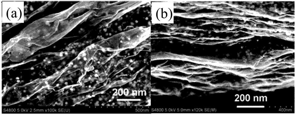
Metal NPs with different shapes can also be directly decorated on 2D materials without adding a linker agent with the assistance of waves, which is different from the chemical reduction and electrochemical methods.158 Wang et al. reported the hybrid nanostructures of Ag NPs/graphene with different shapes.158 As shown in Fig. 5(a), expandable graphite was heated to 950 °C for 20 s under Ar gas to obtain expanded graphite, which was subjected to sonication in NMP.158 The resulting dispersion was centrifuged, and the well-dispersed graphene solution was obtained by collecting the top half of centrifuge tube's contents. The pre-synthesized Ag NPs (dispersed in ethanol) with different morphologies were mixed with the contents resulting from centrifugation. After sonication of the mixture, the resultant suspension was held steady for several hours, and the hybrid nanostructures of Ag nanospheres/graphene (Fig. 5(b)), Ag nanocubes/graphene (Fig. 5(c)), and Ag nanoplates/graphene (Fig. 5(d)) were formed through spontaneous adsorption of Ag NPs onto the pristine graphene surface.158
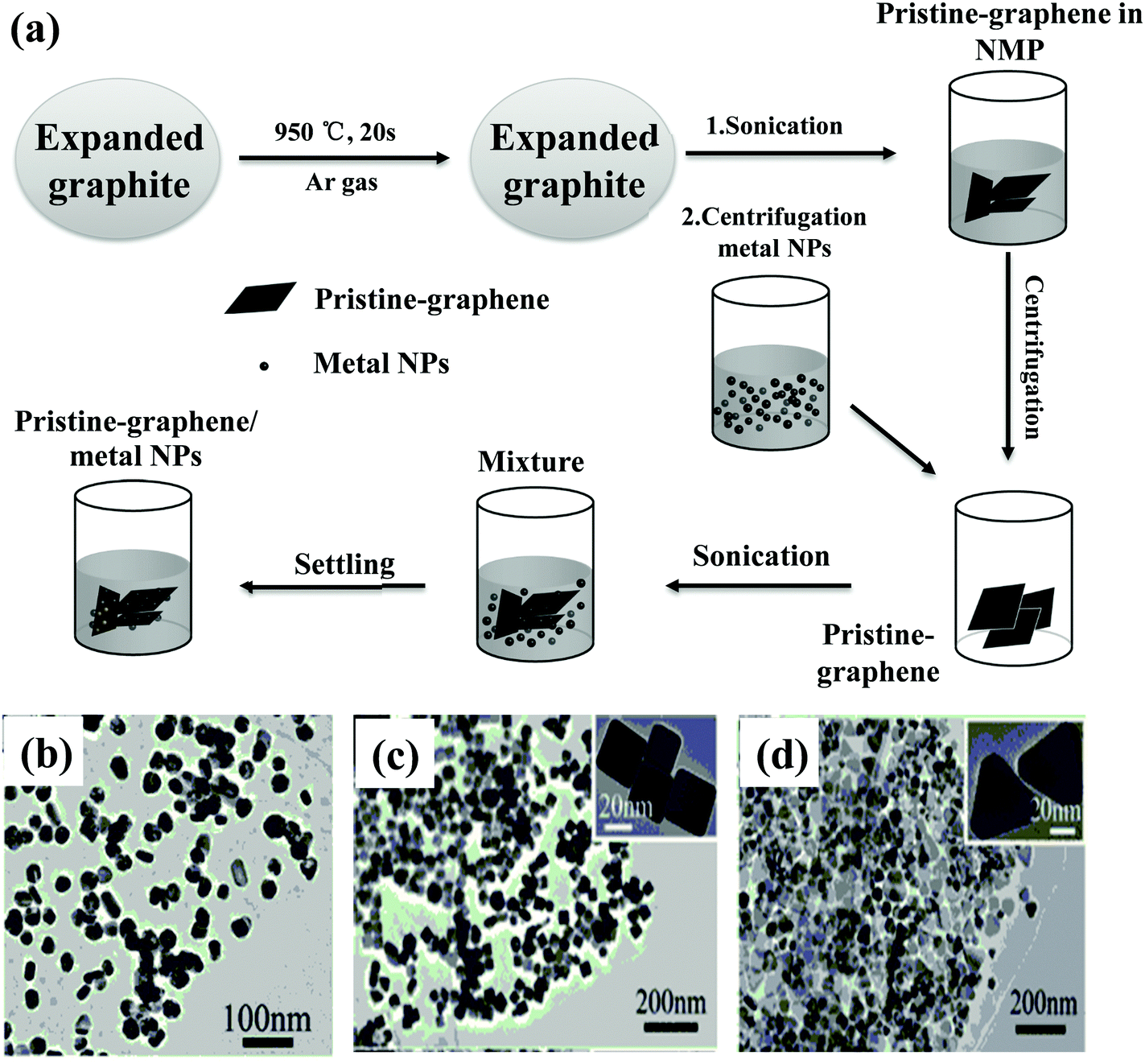 | ||
| Fig. 5 (a) Schematic illustration of the synthesis of the hybrid nanostructures of metal NPs/graphene, and the corresponding TEM images of (b) Ag nanospheres/graphene, (c) Ag nanocubes/graphene, and (d) Ag nanoplates/graphene hybrids. Reproduced with permission.158 Copyright 2013, Wiley-VCH Verlag GmbH & Co. KGaA, Weinheim. | ||
2.2 Preparation of hybrid nanostructures of metal nanostructures/2D materials
The hybrid nanostructures of metal nanostructures/2D materials are used in plasmon-enhanced optical signals, including SERS, plasmon-enhanced photoluminescence (PL),159,160 and plasmon-enhanced photodetection, because of their fabrication technique and 2D structural features.161–163 Thus, there are some functional requirements for the design and manufacture of these hybrid nanostructures in addition to some specific demands depending on a particular application. First, the metal nanostructures should have a strong plasmonic effect, and the 2D material film should be of high quality. Second, avoiding damage to the two components and ensuring tight contact between the two components are critical during the integration of metal nanostructures and 2D materials. Compared to the preparation of hybrid nanostructures of metal NPs/2D materials, which can be obtained by various methods, the fabrication of hybrid nanostructures of metal nanostructures/2D materials primarily uses a physical method. Three steps are needed: fabrication of the metal nanostructures, preparation of the 2D materials, and integration of the metal nanostructures and 2D materials. Thus, obtaining the two single components is a prerequisite for these hybrid nanostructures. After preparation of the two individual components, realizing the integration of the metal component and the 2D component becomes the crucial step.In recent years, simple hybrid nanostructures with a single metal component and a single 2D component have been reported by placing the 2D materials on top of the pre-fabricated metal nanostructures164–168 or by directly fabricating the metal nanostructure on top of the 2D materials.161–163,169–174 The advantage of the former method is that it is easier to obtain the hybrid nanostructures and very suitable for studying the plasmon-enhanced optical signals and fabricated tunable plasmonic resonance. As shown in Fig. 6(a), PMMA can be first spin-coated on top of pre-prepared graphene grown on the Cu foil, and the Cu foil is then etched away. Then, the graphene is transferred to cover the Au voids, which have been fabricated by nanosphere lithography (NSL) in advance.167 After the PMMA covering the graphene has been dissolved, the hybrid nanostructures of metal voids/graphene can be obtained. Following a similar procedure, a monolayer graphene covering an annular gap array of Au with a gap size of 2 nm as a hybrid device for terahertz (THz) transmission was fabricated (Fig. 6(b)).165 In addition to the hybrid nanostructures of metal nanostructures/graphene, hybrids of metal nanostructures with other 2D materials have also been reported, such as single-layered MoS2 coated with Au nanorod arrays fabricated by combining electron beam lithography (EBL), chemical vapor deposition (CVD), and a transfer technique.175 The integration process and quality of 2D materials have substantial effects on the device performance and application. Two key points should be considered. (1) The roughness of the metal nanostructures should be controlled to reduce wrinkles or other damage to the 2D materials. (2) The surface wetting properties of the metal nanostructures and 2D materials are also significant issues that affect the integration of these materials. For example, although the typical metal films and graphene are hydrophobic, it is hard to scoop the graphene floating on the water using metal nanostructures. Thus, surface decoration is necessary to modify hydrophobicity.
 | ||
| Fig. 6 (a) Schematic illustration of the metal voids/graphene hybrid nanostructures by transferring graphene to the top of the metal voids. Reproduced with permission.167 Copyright 2013, American Chemical Society. (b) Schematic diagram of THz transmission coupled to monolayer graphene onto an annular gap array with a gap size of 2 nm. Reproduced with permission.165 Copyright 2015, Wiley-VCH Verlag GmbH & Co. KGaA, Weinheim. (c) Schematic of an end-to-end coupled antenna array, Reproduced with permission.176 Copyright 2013, American Chemical Society. (d) Schematic illustration of a single Au heptamer sandwiched between two monolayer graphene sheets. Vg is the gate voltage used to dope electrostatically the graphene, and (e) the corresponding SEM image of the as-fabricated device before (left) and after (right) deposition of the second graphene layer. Reproduced with permission.178 Copyright 2013, American Chemical Society. The scale bar of the inset of (e) is 100 nm. | ||
In the latter method, the metal nanostructures are fabricated on the 2D materials. As shown in Fig. 6(c), a nanoarray of Au nanorods made using the focused ion beam (FIB) technique is placed on top of graphene.176 The pre-obtained graphene can be realized by transferring the CVD-grown graphene from other substrates. Through a similar method, the hybrid nanostructures of metal nanostructures/MoS2 materials have also been reported, such as hybrid nanostructures of Ag bowtie nanoantenna arrays sitting on top of a chemically grown MoS2 monolayer160 and Ag nanodisk arrays placed on top of a MoS2 monolayer.177 From the viewpoint of fabrication, this method is also very easy, and this type of architecture is very compatible for plasmon-enhanced optoelectronics and electrically tunable plasmonic resonance applications. Compared to the former method, the latter avoids the transfer of 2D materials to metal nanostructures and reduces the formation of wrinkles in 2D materials. The second method involves the fabrication of metal nanostructures directly on top of 2D materials; efficiently realizing the metal nanostructures and avoiding damage to 2D materials are key technological issues.
In addition to simple hybrid nanostructures composed of single parts of metal nanostructures and single parts of 2D materials, relatively complicated hybrid nanostructures have also been reported.179–181 Recently, Halas et al. designed the Au heptamers sandwiched between monolayer graphene sheets.178 As shown in Fig. 6(d), the first graphene monolayer was placed on top of the SiO2 substrate; then, Au heptamer nanostructures were fabricated on the substrate. Afterward, a second graphene monolayer was transferred onto the top of the Au nanostructures. This complicated hybrid nanostructure can be designed for optoelectronics. Fig. 6(e) shows the corresponding SEM images of the as-fabricated device, the Au nanoarrays of heptamers are sitting on the first graphene monolayer (left). After the second graphene monolayer is placed on top of the Au heptamers, graphene wrinkles can be observed around the edge of the Au heptamers (Fig. 6(e)).178 In addition, other complicated hybrid nanostructures have been designed and fabricated. To achieve an ultrahigh field enhancement and photoresponse, Paria et al. reported arrays of plasmonic dimers separated by atom-thick graphene.182 They first made Ag NPs on top of silica spheres using oblique angle deposition. A single-layered graphene was transferred on top of the Ag NPs using the standard graphene transfer protocols, and the second layer of Ag NPs arrays was deposited on graphene using the same oblique angle deposition. After an annealing treatment, the Ag NP dimers with graphene as the nanospacer were obtained.182 Because the distance is tiny (i.e., 0.34 nm), very strong plasmonic coupling can be achieved, which can be used for high-performance photodetectors. Hybrid graphene/h-BN/Ag nanodisc nanoarrays have also been fabricated to study plasmon-induced optical anisotropy. h-BN introduced as a sub-nanospacer layer functioned as an effective barrier to electron transfer when the light–matter interaction between graphene and metal nanostructures was studied.183 Compared to the simple hybrid nanostructures, relatively complicated hybrid nanostructures will possibly produce a stronger light–matter interaction or possess additional functions for various applications. The design of other complex hybrid nanostructures with additional or specific features will become increasingly important and interesting.
2.3 Summary of preparation of hybrid nanostructures of metal nanomaterials/2D materials
For the preparation of hybrid nanostructures of metal NPs/2D materials, six methods have been discussed and compared, including physical deposition, chemical reduction, photocatalytic reduction, an electrochemical method, a solvothermal method, and a wave-assisted reduction method. The features, disadvantages, and applications have been summarized in Table 1. The physical deposition of metal NPs directly on the 2D materials does not require any chemical agents (i.e., reduction agents) and avoids the introduction of any additional residuals in the hybrid nanostructures. However, the disadvantage of this method is that the size and distribution of the metal NPs deposited on the 2D materials are difficult to control.63 Compared to the physical deposition of metal NPs on 2D materials, the other five methods are solution-processed, which, to some extent, reduces the fabrication cost. Fabricating hybrid nanostructures with high specific surface areas is another advantage of these solution-processed methods.74–81 The possible drawback of the solution-processed method is that some additional residuals or impurities will be introduced during the preparation process.103–111 In addition, solution-processed 2D materials always have some defects that will affect the electronic properties of hybrid nanostructures. Among these methods, chemical reduction is the primary method. By introducing another driving force as an assisting agent into the chemical reduction system, new and advanced methods have been developed, e.g., introducing light for photocatalytic reduction, introducing electricity for electrochemical processes, introducing high pressure and high temperature for solvothermal methods, and introducing waves for the wave-assisted reduction technique. For chemical reduction and electrochemical reduction, additional linkers added into the reduction system are beneficial to avoid the aggregation of the hybrid nanostructures and to keep the metal NPs tightly anchored on the 2D materials.103–111,135,142 When these solution-processed methods are applied, various structural features are observed. For example, subtle metal NPs are always synthesized and well decorated on the 2D materials when using the photocatalytic reduction method, if the experimental parameters are well controlled.174 The layered hybrid nanostructures with alternating metal NPs and 2D materials are inclined to be fabricated when electrochemical deposition is applied.141| Methods | Features | Disadvantages | Applications |
|---|---|---|---|
| Physical deposition | Fast, efficient, without addition species | Size and distribution of metal NPs are not easy to control | SERS, PL, PD |
| Chemical reduction | Simple, facile, efficient, large surface area | Assistant agent needed, impurities introduced | SERS, PL, photocatalytic reaction, interlayer of solar cells |
| Photocatalytic reduction | Green, facile, large surface area, metal NPs with small size well distributing on the 2D materials | Light intensity and illumination time have significant influences on the synthesis of the hybrids | SERS, PL, photocatalytic reaction, interlayer of solar cells |
| Electrochemical method | Simple, green, large surface area, layered hybrid nanostructures with alternating metal NPs and 2D materials | Assistant agent needed | SERS, PL, photocatalytic reaction, interlayer of solar cells |
| Solvothermal method | Simple, cost-effective, facile, large surface area | Hybrids suffer from a certain degree of aggregation | SERS, PL, photocatalytic reaction, interlayer of solar cells |
| Wave-assisted reduction | Rapid, green, facile, low-consuming energy, large surface area | Synthesis of hybrids is sensitive to wave intensity and radiation time | SERS, PL, photocatalytic reaction, interlayer of solar cells |
For the preparation of hybrid nanostructures of metal nanostructures/2D materials, two crucial points should be emphasized: realizing unique metal nanostructures with specific requirements using lithography methods such as EBL, FIB, and NSL175 and successfully integrating the metal nanostructures with 2D materials without damage to the physical and chemical properties of the two components.
We should mention again the particular requirements for the preparation of hybrid nanostructures of metal/2D materials, which is dependent on the plasmon-enhanced application. For example, the large specific surface area is beneficial to the plasmon-enhanced photocatalytic reaction. To achieve this goal, all of the solution-processed methods are possible. Optical sensitivity and selectivity are necessary for photodetectors and should be obtained using physical deposition to design precisely the hybrid nanostructures of metal nanostructures/2D materials.178 Restrained electron transfer for plasmon-enhanced PL can be realized by introducing an additional dielectric layer between the metal nanomaterials and 2D materials.53,70,71
However, there are currently several difficulties in the fabrication of hybrid nanostructures. In the hybrid nanostructures of metal nanomaterials/2D materials, the metal nanomaterials are not tightly anchored on the 2D materials. The poor contact between the metal nanomaterials and 2D materials will greatly block the charge transfer. In addition, the morphology and structures of the metal nanomaterials and the film quality of the 2D materials are always destroyed during the integration of the two components, which will ultimately have an adverse impact on device performance. To tackle these problems, a fundamental understanding of the physical and chemical properties of the two components is necessary. Improving the existing preparation techniques and developing new fabrication methods are expected.
3. Optical properties of the hybrid nanostructures of plasmonic metal/2D materials
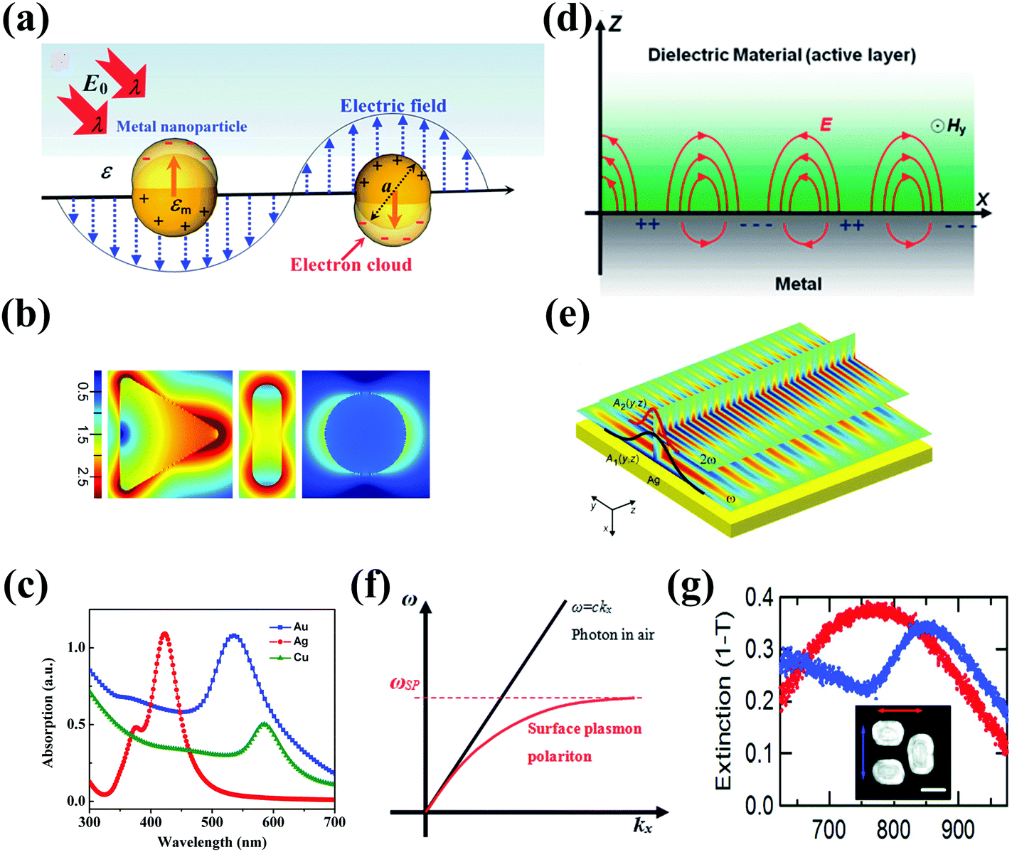
To discuss the optical properties of the hybrid nanostructures of metal/2D materials, we should understand the fundamental properties of the individual noble metal component and the 2D materials, respectively. Considering that each component has already been widely reported and reviewed recently,11,25,36,43,48,58,59,70,73,184–188 we will briefly introduce the plasmonic effects derived from metal NPs and nanostructures and the various properties of 2D materials and then mainly review the optical properties of the hybrid nanostructures in this section.3.1 Plasmonic effects from metal NPs and metal nanostructures
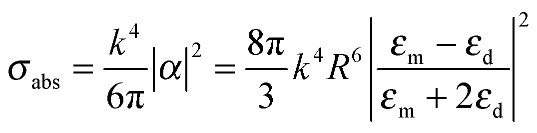
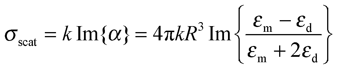
Metal NPs (e.g., discrete nanospheres, nanorods, nanocubes, and nanoprisms) and nanostructures (e.g., arrays of nanopatterns, metal slits) that reveal strong light–matter interactions between the electromagnetic field and free electrons make them useful materials for achieving plasmonic effects.59 The principle of the metal plasmonic effect can be understood by comparison with a simple harmonic oscillator. Metals can be regarded as heavy, positive nuclei surrounded by a cloud of free electrons. When an oscillating optical electric field is incident on the metal acting as the applied force, the electrons surrounding the metal are driven and move along the field direction. At the same time, the Coulombic attraction between the delocalized electron cloud and the nuclei acts as the restoring force, which is opposite to the displacement of electrons. At a certain resonant frequency, the oscillations caused by the Coulombic attraction become in phase with the oscillating electric field. As a result, the incident light is absorbed by the metal; effective energy is stored in the metal; and a very strong electric field is produced around the metal. Typically, plasmonic effects can be divided into two types: the localized surface plasmon (LSP) effect and the surface plasmon polariton (SPP) effect.189,190 Materials that can support the plasmonic effect in the visible and near-infrared regions are required to have free charge-carrier concentrations of up to 1021 cm−3.191,192 Metals, such as Au, Ag, and Cu with enough free electrons, are suitable materials for supporting the plasmonic effect in the visible and near-infrared regions.70The LSP effect is mainly attributed to the confined electrons on the surface of the metal NPs.59 The modes of non-propagating plasmons primarily arise from interactions between the incident light and the sub-wavelength metal NPs.185,193 The underlying physics is that the curved protuberance from the NPs will generate an efficient restoring force on the driven electrons, which will induce a resonance and finally amplify the electromagnetic field in the near-field region outside the metal NPs (see Fig. 7(a)).193 The Mie theory analytically solving Maxwell's equations can be utilized for characterizing the excitation of resonance modes. The extinction (σext), scattering (σscat) and absorption cross section (σabs) of metal nanospheres are given as follows:194
 | (1) |
 | (2) |
| σabs = σext − σscat | (3) |
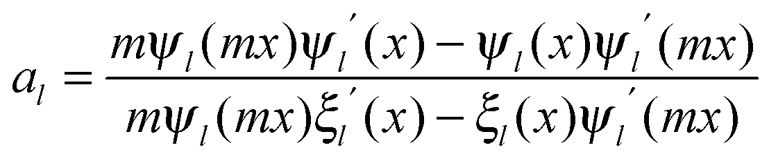
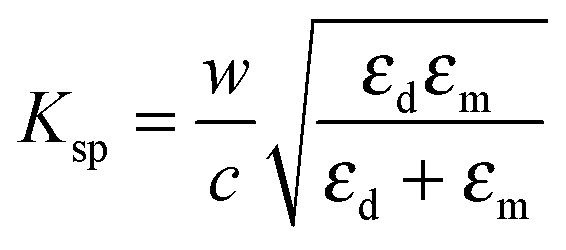
in which ψn and ξn are the Riccati–Bessel cylindrical functions, k is the wavenumber of the incident light in the dielectric medium, the size parameter is x = kR, R is the radius of metal nanospheres and m = nm/nd is the relative refractive index. Here,

 , εm and εd are the permittivities of metal nanospheres and the surrounding dielectric medium, respectively.
 | ||
| Fig. 7 (a) Illustration of the LPR effect on nanospheres. Reproduced with permission.193 Copyright 2014, Royal Society of Chemistry. (b) The electric field intensity enhancement of differently shaped Au nanocrystals, including from left to right the nanoprism with an edge length of 87 nm and a thickness of 10 nm, a nanorod with a length of 103 nm and a diameter of 30 nm, and a nanosphere with a diameter of 50 nm. Reproduced with permission.70 Copyright 2014, Wiley-VCH Verlag GmbH & Co. KGaA, Weinheim. (c) The absorption spectra of different metal components, including Au nanospheres, Ag nanospheres, and Cu nanospheres with a diameter of 50 nm. (d) Illustration of the SPP effect between the metal and dielectric layer. Reproduced with permission.193 Copyright 2014, Royal Society of Chemistry. (e) The propagating SPP near-field profile of grating with soliton geometry, Reproduced with permission.199 Copyright 2015, IOP Publishing. (f) Dispersion curve of a typical SPP mode, where a momentum mismatch exists between the light and the SPP. Reproduced with permission.193 Copyright 2014, Royal Society of Chemistry. (g) The extinction spectra of the dolmen nanoantenna shown in the inset of the panel. The structure (200 nm side) is illuminated by light with different polarization (red and blue arrows). Reproduced with permission.203 Copyright 2009, American Chemical Society. | ||
When the nanoparticle size is much smaller than the incident wavelength, the metal nanoparticle can be considered as a dipole and the electrostatic approximation is an efficient tool for characterizing and understanding the resonance of the metal nanoparticle. The polarizability (α) of a metal nanosphere can be expressed as follows:
 | (4) |
 | (5) |
 | (6) |
| σext = σabs + σscat | (7) |
The resonant properties of the LSP effect can be efficiently modified by changing the shape, material composition, and size of the metal NPs.44,45,54 Regarding the shape, a high field enhancement occurs around the curvature of metal NPs. As shown in Fig. 7(b), the Au NPs with different shapes show different field intensity increases. Compared to Au nanospheres, nanoprisms and nanorods show stronger field enhancements around the tip regions. In general, the maximum field enhancement for plasmonic metal NPs reported from theoretical calculation ranges from ca. 50 to ca. 10![[thin space (1/6-em)]](https://www.rsc.org/images/entities/char_2009.gif) 000, strongly dependent on the metal shapes.70 In addition, the shape of plasmonic metal NPs also affects the plasmonic resonance. By changing the geometry, the LSP peak can be tailored from the violet to the visible region and the infrared region.195 Recently, a novel black plasmonic colloidosome assembled from Au nanospheres has been reported, which showed broadband absorption.196 Regarding the metal component, the permittivity of materials has direct effects on the plasmonic resonance. Typical plasmonic metal components including Au, Ag, and Cu have different permittivities. As a result, the well-dispersed Au NPs, Ag NPs, and Cu NPs with a diameter of 50 nm show an LSP peak at 512 nm, 400 nm, and 576 nm, respectively (Fig. 7(c)). Regarding the size of plasmonic metal NPs, in general, smaller metal nanospheres (i.e., 20 nm Au) are primary absorbers due to a strong near-field enhancement, whereas relatively large metal nanospheres (i.e., 80 nm Au) have a more noticeable scattering due to far-field enhancement.53 In addition, the environment surrounding the metal component also has a strong effect on the plasmonic resonance. A change in the dielectric constant will lead to a shift in plasmonic resonance. The large dielectric constant of a medium around the plasmonic metal results in a more obvious red-shift of plasmonic resonance. Based on this principle, the plasmonic metal can be used as an ultrasensitive sensor for detecting environmental pollutants and bio-molecules.197
000, strongly dependent on the metal shapes.70 In addition, the shape of plasmonic metal NPs also affects the plasmonic resonance. By changing the geometry, the LSP peak can be tailored from the violet to the visible region and the infrared region.195 Recently, a novel black plasmonic colloidosome assembled from Au nanospheres has been reported, which showed broadband absorption.196 Regarding the metal component, the permittivity of materials has direct effects on the plasmonic resonance. Typical plasmonic metal components including Au, Ag, and Cu have different permittivities. As a result, the well-dispersed Au NPs, Ag NPs, and Cu NPs with a diameter of 50 nm show an LSP peak at 512 nm, 400 nm, and 576 nm, respectively (Fig. 7(c)). Regarding the size of plasmonic metal NPs, in general, smaller metal nanospheres (i.e., 20 nm Au) are primary absorbers due to a strong near-field enhancement, whereas relatively large metal nanospheres (i.e., 80 nm Au) have a more noticeable scattering due to far-field enhancement.53 In addition, the environment surrounding the metal component also has a strong effect on the plasmonic resonance. A change in the dielectric constant will lead to a shift in plasmonic resonance. The large dielectric constant of a medium around the plasmonic metal results in a more obvious red-shift of plasmonic resonance. Based on this principle, the plasmonic metal can be used as an ultrasensitive sensor for detecting environmental pollutants and bio-molecules.197
Another type of plasmonic effect is the SPP effect, which typically propagates evanescent waves bound around interfaces between metal nanostructures and dielectrics due to the coupling of the electromagnetic fields and the oscillation of the electrons in the metal nanostructures (Fig. 7(d)).198 Based on Maxwell's equations, the dispersion relationship can be described by the following equation:198
 | (8) |
 | (9) |
To conclude, of the optical properties of plasmonic nanomaterials including metal NPs and metal nanostructures, the first important one is that plasmonic nanomaterials exhibit very strong light–matter interactions under resonant excitation.207 Very significant absorption and scattering at the LSP and SPP wavelengths can be achieved. The absorption-induced scattering and surface plasmon out-coupling have also been reported, which make the optoelectronic application of metasurfaces practical.208 Second, both absorption and scattering cross-sections can be tailored by changing the size, shape, metal composition, and environment of the metal NPs and metal nanostructures over a broad wavelength region from violet and visible to infrared wavelengths.70,209 Another important property of plasmonic NPs and nanostructures is electric field localization, which enables plasmonic resonance to break the diffraction limit and trap light in a nanoscale region.54,210–213
3.2 Properties of 2D materials
As discussed above, the unique structures and properties of 2D materials enable them to be excellent building blocks not only for designing hybrid nanostructures but also in promising photonic and electric devices. To better understand and create the hybrid nanostructures of metals/2D materials, various properties of 2D materials, including the mobility, conductivity, absorbance, mechanical flexibility, and specific surface area, will be comprehensively discussed in this section.3,271Graphene is a zero-bandgap semiconductor with the highest carrier mobility at room temperature (∼40000 cm2 V−1 s−1) reported to date.214 The schematic structure and electric band structure of graphene are shown in Fig. 8.272 The sheet resistance Rs of a graphene monolayer is ∼62.4 Ω sq−1, enabling it to hold a potential in high-frequency electronic devices and highly transparent conductive electrodes.215 Because of its emergent electronic structure with massless Dirac fermions, ballistic carrier transport was achieved in suspended graphene.216 Regarding its absorbance, the optical conductivity is mainly contributed by interband carrier transitions in the visible range. For the cases of intrinsic or lightly doped graphene, the absorbance is constant (∼2.3%) in the visible range.3,6 In contrast, the optical conductivity of graphene in the THz range is primarily contributed by intraband scattering.3,6 Compared to metal nanomaterials showing a plasmonic effect in the near-infrared and visible regions, graphene exhibits a tunable plasmonic effect due to its ability for low losses and high confinement in the THz range and the mid-infrared range.217–223 Through chemical and electrical doping, the permittivity (i.e., charge density and conductivity) and plasmonic characteristics (i.e., confinement and wavenumber) of graphene can be tuned.224 Therefore, graphene can be potentially used for optical modulators. A possible coupling between metal nanomaterials and graphene can also be achieved if the plasmonic resonance of their wavelengths is tuned to overlap each other.225 Furthermore, as one of the strongest materials, the 3D Young's modulus and the intrinsic breaking strength of graphene can reach up to ∼1.0 TPa and ∼130 GPa, respectively, making it a promising material for flexible optical and electronic devices. Graphene also has a large surface area. As recently reported, graphene nanomaterials with a surface area of 2150 m2 g−1 were synthesized using a chemical exfoliated method, indicating that graphene has prospective applications in photocatalytic reactions, sensors, and solar cells.
 | ||
| Fig. 8 The schematic structures of graphene and MX2 type crystals. Reproduced with permission.272 Copyright 2015, Royal Society of Chemistry. The schematic structures of h-BN. Reproduced with permission.73 Copyright 2014, Royal Society of Chemistry. The electric band structures of graphene and MoS2. Reproduced with permission.272 Copyright 2015, Royal Society of Chemistry. The electric band structures of h-BN. Reproduced with permission.273 Copyright 2015, Royal Society of Chemistry. | ||
GO is a type of intermediate material between graphite and graphene.226 The structure and properties of GO are different from that of graphene because oxygen bonding forms sp3 hybridization on graphene.226 The introduction of oxygen atoms, which have a larger electronegativity than carbon atoms, causes GO to exhibit distinct p-type doping properties.227 The bandgap of GO is strongly affected by the oxidation level.227 In addition, the GO bandgap can also be tuned by doping or functionalization.228,229 Furthermore, GO synthesized by solution-processed methods exhibits one of the largest specific surface areas among the 2D materials. Both the structural features and related chemical and physical properties make GO an ideal photocatalyst for water splitting, optical sensing for biotechnology,230–234 and buffer layers for photovoltaics.235,236
Another class of 2D materials, semiconducting TMD monolayers, have a direct band gap (Fig. 8).272 As two typical examples of TMDs, the MoS2 multilayer is an n-type semiconductor with a reported mobility of 980 cm2 V−1 s−1, and WSe2 exhibits a p-type semiconductor property with a recorded mobility of 500 cm2 V−1 s−1. A single-layer MoS2 field effect transistor (FET) shows a mobility of 10–30 cm2 V−1 s−1 and an on/off ratio exceeding 106.237,238 Compared to that of graphene, the conductivity of 2D TMDs is very low. A MoS2 monolayer has an absorbance of 5–10%, which is relatively higher than that of graphene, Si, and GaAs of the same thickness. Therefore, 2D TMDs can potentially be used for photoelectronic devices and photocatalytic reactions. In addition, the MoS2 monolayer has a direct band gap of 1.8 eV. Specifically, MoS2 can produce a high PL, which enables MoS2 as an emitter and optical imager in biotechnology.239,240 Moreover, 2D TMDs also have relatively large surface areas. For instance, a recently reported MoS2 showed a specific surface area of 210 m2 g−1. In summary, based on the properties of 2D TMDs, including a moderate mobility, good absorbance, low conductivity, and large surface area, MoS2 can be applied in sensing,241–243 photovoltaics,244–246 optical catalytic reactions,247,248 and photodetector applications.249–257
Recently, much attention has been focused on the optical properties of h-BN insulators.17,73,258 The schematic structure and electric band structure of h-BN are shown in Fig. 8.73,273 They have a wide bandgap of ∼5.9 eV and do not exhibit any optical absorption in the visible region of 390–700 nm. Compared to plasmon polaritons in graphene, the phonon polaritons in h-BN possess extremely high confinement and even lower loss.259,260 h-BN shows natural hyperbolicity,261,262 which can potentially be used for strong spontaneous deep UV emission enhancement around ∼210–220 nm,258 Raman enhancement,263 and biosensors.154 Recently, scanning near-field optical microscopy (SNOM) has been adopted for studying the plasmonics of graphene in the mid-infrared region.264–268 By combining graphene and h-BN to form a heterostructure, highly confined low-loss plasmons can be observed using SNOM which shows high sensitivity.259 A graphene moiré superlattice has been created by placing a graphene monolayer on an h-BN film, producing collective oscillations of electrons contributing to infrared plasmons.269,270
3.3 Properties of hybrid nanostructures of metal/2D materials
Because of the strong plasmonic effect induced by the metal nanomaterials in the hybrid nanostructures, some properties of the 2D material component, e.g., photocatalysis, PL, and optoelectronics, will be altered and enhanced by the metal part. To date, the hybrid nanostructures of metal nanomaterials/2D materials have been widely explored in various plasmon-enhanced applications, including plasmon-enhanced optical signals (i.e., PL, SERS, and SPR sensors), plasmon-enhanced photocatalytic reactions (i.e., photodegradation of organic pollutants and water splitting), and plasmon-enhanced optoelectronic devices (i.e., solar cells and photodetectors). We will discuss these applications in the section on plasmon-enhanced applications (Section 4). On the other hand, the plasmonic resonance of the metal component will be greatly tailored after hybridization with the 2D material component because plasmonic resonance is highly dependent on the dielectric function of the surrounding medium.59 In addition, an active plasmon-exciton reaction triggers the “hot electron” transfer from the metal NPs to the 2D materials, which will dampen the plasmonic resonance of metal nanostructures or change the absorption of the 2D materials, etc.274–277 In this section, three typical types of optical properties of the hybrid nanostructures will be reviewed, including the synthetically tunable plasmon resonances of metal NPs, the electrically tunable plasmon resonances of metal nanostructures, and the tunable absorption of 2D materials.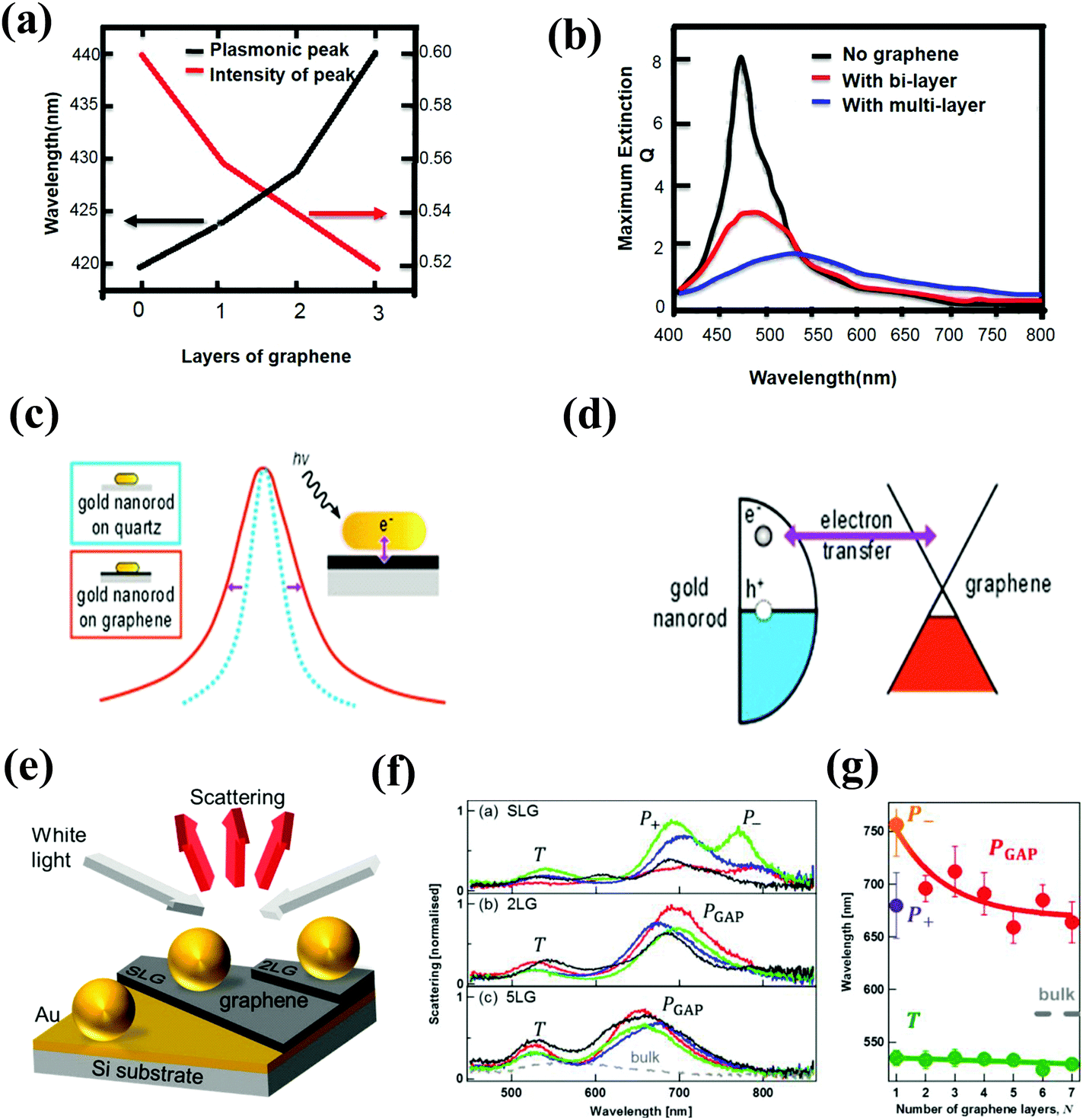 | ||
| Fig. 9 (a) Plasmonic resonance frequency and amplitude with respect to the number of graphene layers, and (b) simulated Q-values of Ag disks with 10 nm thickness and 40 nm diameter without graphene, with a 0.7 nm graphene layer, and with a 2 nm graphene layer between the Ag disk and the glass substrate. Reproduced with permission.278 Copyright 2012 Wiley-VCH Verlag GmbH & Co. KGaA, Weinheim. (c) Schematic of the plasmon linewidth in plasmonic nanorods with or without graphene, and (d) a schematic energy diagram illustrating charge transfer between an Au nanorod (left) and graphene (right) following plasmon-induced hot electron generation. Reproduced with permission.281 Copyright 2013, American Chemical Society. (e) Schematic of a graphene sandwiched plasmonic coupling system, (f) dark-field single particle scattering spectra of four Au NPs on SLG, 2LG, and 5LG, and (g) resonance wavelength of the plasmonic T, P+, P−, and PGAP modes for increasing the numbers of graphene layers, N. Reproduced with permission.284 Copyright 2013, American Chemical Society. | ||
In addition, if the imaginary part of the dielectric function of the 2D nanomaterial component is large, such as graphene (ng = 2.4 + i·1 for graphene),278 the LSPR of the metal component can be drastically dampened and become broad. As shown in Fig. 9(b), the plasmonic resonance of Ag NPs on graphene is dampened and broadened to some extent with increasing graphene layers, compared to Ag NPs on the bare glass. The intensity of plasmonic resonance is decreased from 0.60 to 0.52 after 3 layers of graphene are inserted between the metal NPs and the glass.278 This variation may be primarily attributed to the energy (or hot electrons produced via plasmon excitation) transfer from Ag NPs to graphene, which dissipates the electric-field concentration on the surface of Ag NPs, resulting in a decrease in the amplitude of their plasmonic resonance. Recently, a strong coupling through charge transfer and local electric fields was proven in the hybrid nanostructures of metal NPs/graphene.274–277 The time scale of energy relaxation after photo-excitation and the efficiency of electron transfer between the Au NPs and graphene were determined by comparing the line widths obtained from the individual metal NPs on glass and graphene using single-particle dark-field scattering and PL spectroscopy. As shown in Fig. 9(c), the plasmonic resonance of the metal NPs exhibited a 13 nm broadening due to the presence of graphene. Analysis of the plasmonic line width yields an average electron transfer time of 160 ± 30 fs, and charge transfer between the Au nanorods and the graphene support occurs with an efficiency of ∼10%.281 Understanding the hot electron transfer is very important for future applications of light harvesting with plasmonic metal NPs and efficient hot electron acceptors in plasmon-assisted chemical reactions. On the contrary, it is not beneficial for plasmon-enhanced sensors if the damping of the metal NP plasmons on the graphene layer exists, which reduces the localized light intensity. Inserting a thin dielectric such as HfO2, Al2O3, or water between the graphene layer and the metal NPs is an efficient method to reduce the plasmon damping process on graphene.282,283
Although the plasmonic resonance of metal NPs is tunable by simply placing the metal NPs and graphene together, i.e., the metal NPs are placed on top of graphene, the shift is too slight to attain adequate light modulation. Based on experimental studies of plasmons in NP dimers, the plasmonic resonance can also be tailored through a spacer component between the NPs.285–296 Recently, graphene was introduced into an NP-film coupling system to realize substantial spectral tuning in the visible-to-near-infrared region.284,297 As shown in Fig. 9(e–g), the hybrid nanostructures are composed of a film/spacer/NP coupling system by introducing different layers of graphene between the upper Au NPs and the lower Au film as a sub-nanospacer. The coupling mechanism for this system is mainly due to the plasmonic coupling between the particle and its image within the metal substrate.284 From the scattering spectrum (Fig. 9(f)), three plasmonic peaks can be observed when a graphene monolayer is used as the nanospacer, which is attributed to three modes, transverse plasmons (T) at approximately 500–600 nm, dipolar resonance (P−, P− = PCTP − PGAP), and quadrupolar plasmonic resonance (P+, P+ = PCTP + PGAP) at approximately 700–900 nm.298,299 The PCTP presents the charge-transfer plasmon (CTP) between the upper Au NPs and their image. The PGAP plasmon gives the dipole located near the gap (“GAP plasmon”). As the layer of graphene is increased from 1 to 6, the P+ disappears, and the dipolar resonance blue-shifts undoubtedly occur from 800 nm to 650 nm (Fig. 9(f) and (g)).284,297 Thus, a wavelength shift of nearly 150 nm is observed, which implies that the plasmonic graphene-sandwiched hybrid design is a very efficient light modulator. The screening effect of graphene plays a significant role in modulating the plasmonic resonance.297 The nature of the charge transfer and gap plasmon hybridization depends on the conductivity of the gap; and thus, different effects may be expected for graphene and other 2D materials such as h-BN. It is worth saying that the system of NP-film coupling system is used as a model system to provide a very controlled and experimentally reproducible equivalent of an Au NP dimer. Otherwise, it is very difficult to achieve a coupling system with a sub-nanometer gap. Therefore, understanding the tunability of plasmonic resonance in the NP-film coupling system by 2D materials is very important because an efficient modulation of light has a high potential for perfect absorbers,300–302 Raman enhancement,303,304 and light-harvesting applications.182
Other 2D materials such as MoS2 and h-BN also have the ability to tailor the plasmonic resonance of metal NPs because the 2D materials can affect the surrounding media of the metal NPs when they hybridize with the metal NPs.126,155 In addition, electron transfer from the metal to the 2D materials is also possible.305
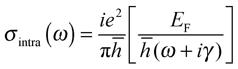 | (10) |
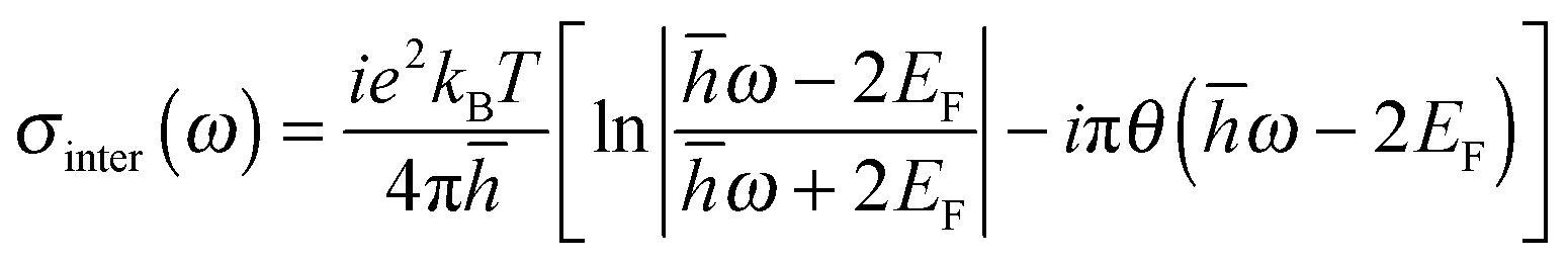 | (11) |
Due to the Pauli blocking of the interband transition, the Fermi level of a single layer of graphene can be electrostatically controlled by applying different gate voltages to the FET structure. Regarding eqn (10) and (11), the surface conductivity of graphene is largely dependent on the Fermi level EF, and EF can be modified in situ by the applied back-gate voltages determined by the following equation:
 | (12) |
With the capability to modulate the Fermi level by applying different gate voltages, the in situ control of the optoelectronics becomes possible. Recently, the modulation of the plasmonic resonance frequency of metal nanostructures has been successfully realized by exploiting the electrically tunable optical transitions of graphene in the hybrid metal–graphene system.306 By tailoring the Fermi level of graphene, the plasmonic resonance range can be efficiently modulated over a broad region from the terahertz (THz) and infrared to the visible wavelength region.172,307–309
The tunable resonance around the THz region in the metal/graphene system was first demonstrated by applying a gate voltage.172 The active control of the wave in a range of 0.25 to 2.75 THz was realized based on the coupling of the CVD-grown graphene and the metal materials, as shown in Fig. 10(a). With the FET structure, a modulation depth of 11.5% with an applied bias of 10.6 V was realized by the split-ring resonator that was directly evaporated on top of the large area of graphene grown by CVD (Fig. 10(b)).172 Murphy et al. reported an Au/graphene modulator comprised of a periodic array of narrow slots in a metal layer patterned on top of a graphene sheet. They observed that plasmons from the graphene can be confined to conductive boundaries; thus, a 100% tunable resonance peak in transmission could be predicted.310
 | ||
| Fig. 10 (a) The schematic of the gated CVD graphene/THz-metal material device for back-gate voltages, and (b) the corresponding transmittance normalized to the value near the charge neutral point (CNP) for a selection of spectra. Reproduced with permission.172 Copyright 2013, American Chemical Society. Vg = 0, 2, 4, 6, 8, 10, 11, 12, 13, and 14 V, with ΔVCNP = Vg − VCNP. (c) Reflectivity spectrum from the metal surface without (black) and with graphene calculated using COMSOL simulations. Reproduced with permission.164 Copyright 2013, American Chemical Society. Insets: Charge distribution on the metal surface at the dipolar (right) and the quadrupolar (left) resonances. (d) The main panel shows the modulation depth at different driving voltages, which is normalized to the zero bias transmission (dB μm−1). Reproduced with permission.308 Copyright 2014, American Chemical Society. The gray dashed lines represent the boundary of three regions that correspond to the different injection state of the graphene sheet denoted by I, II, and III. Correspondingly, the three insets show the energy band diagram of graphene in the three regions, and the arrow in the inset of region II represents the absorption of an incident photon. | ||
A broad electrical tuning of a graphene-loaded plasmonic dipole antenna was also demonstrated in the mid-infrared region.307 With the double resonant antenna, the maximum modulation depth can be larger as 30% over a broadband of 650 nm (∼140 cm−1, ∼10% of the resonance frequency).176 In addition, the tunable optical response of the dipole nanoantenna can be switched on and off by different gate voltages. By tuning the Fermi level of graphene, the resonant wavelength at approximately 3200 nm was spilt into two resonant peaks at 2900 nm and 3050 nm due to the in-phase and out-phase coupling between the graphene plasmonic and metal plasmonic.291
The controlled Fano resonance of metal nanostructures around this infrared region was realized in the metal nanostructure–graphene system by applying a gate voltage. The effects of plasmonic damping in a Fano resonance at approximately 2 μm have been observed.174 A blue shift of the Fano resonance of the metal nanostructures without noticeable damping of its spectral sharpness has been observed in the hybrid metal surface/graphene system. As shown in Fig. 10(c), reflectivity spectra from the metal surface without (black) and with graphene obtained using the COMSOL theoretical simulation were plotted.164 The quadrupolar resonance and the dipole resonance (i.e., charge distribution on the metal surface at the dipolar resonance) shifted to the blue wavelength region after graphene was introduced. Then, the blue shift of plasmonic resonance continues after applying a gradually increasing gate voltage. A widely controlled metal surface consisting of plasmonic antennae on graphene integrated with an optical cavity can be created as an electrically tunable perfect absorber and a high speed (20 GHz) and ultrathin (thickness below λ0/10) optical modulator with a modulation depth of 100% over a broad wavelength range (5–7 μm) can be achieved.173
Visible range SPP modulation with a static modulation depth of up to 0.07 dB μm−1 was realized based on a graphene–Ag nanowire hybrid structure (Fig. 10(d)).308 The dual confinement of charge density and electromagnetic energy in the vicinity of the nanowire dramatically enhanced the light–matter interaction and caused the optical response to be in the visible range. By applying more than 25 V to the gate electrode, the charge carrier concentration around the Ag nanowire reached nearly 0.921 × 1014 cm−2, which is very efficient for tailoring the Fermi level for visible light.
 | ||
| Fig. 11 The absorption of a graphene layer when the graphene is placed on the Au/SiO2/Si film and SiO2/Si film. A blue shift (0.35 eV) of the prominent absorption peak was observed. Reproduced with permission.283 Copyright 2015, AIP Publishing LLC. | ||
In addition, the absorption peaks of other 2D materials, such as h-BN, have also been tailored using metal plasmonics in hybrid nanostructures.155 Upon plasmonic excitation, the penetration of the surface of the plasmonic field into the interfacing 2D materials with spatial decay kinetics modifies the dielectric/optical properties of the 2D materials. The typical absorption spectrum of the h-BN nanomaterials at approximately 230 nm is red-shifted to 310 nm after hybridization with Au NPs. The shifting of the absorption peak of the h-BN nanomaterials is attributed to the reduction in the bandgap as a result of the strong near-field energy close to the interface. Electronic rearrangement at the metal/h-BN interface results in the equalization of the Fermi levels and lowering of the energy bandgap relative to the work functions at the interface. Considering that the magnitude of the modified energy bandgap depends on the radially penetrating depth and propagation of transient plasmonic waves at the interface, the optical properties of h-BN can be efficiently tailored using plasmonic nanomaterials.311
First, the plasmonic peak of metal nanomaterials can be tuned after 2D materials are integrated with metal nanomaterials because the plasmonic peak is strongly affected by the surrounding environment.54 Compared to pure metal nanomaterials, the plasmon absorption of the metal nanomaterials in the hybrid nanostructures can be drastically dampened and broadened, mainly due to the “hot electron transfer” from the metal nanomaterials to the 2D materials.274–277 To restrain the “hot electron transfer”, a dielectric layer should be inserted between the metal NPs and 2D materials.274,282,283
Second, the modulation of the plasmonic resonance frequency of metal nanostructures has been successfully realized by exploiting the electrically tunable optical transitions of graphene in the hybrid metal–graphene system. To tailor the Fermi level of graphene by applying different gate voltages with FET structure, the plasmonic resonance range can be efficiently modulated in a broad region from the THz and infrared regions to the visible wavelength region. Currently, the modulation depth is 11.5%, 30% (100% for Fano resonance of metal nanostructures), and 0.07 dB μm−1 in the THz, infrared, and visible wavelength regions, respectively.172,307,308 To achieve more efficient modulation, two key points should be considered: (1) strategically designing specific metal nanostructures that exhibit a resonance frequency near the region to be controlled, and (2) the plasmonic resonance of the designed metal structures should be sensitive to the electrical doping of graphene.
Third, the absorption peak of 2D materials has also been changed in the hybrid nanostructures of metal nanomaterials and 2D materials. These 2D materials are chemically doped through interactions with metal nanomaterials. As a result, the bandgap of 2D materials can be modified. The magnitude of the amended energy bandgap depends on the radially penetrating depth and propagation of transient plasmonic waves at the interface.311 Thus, the optical properties of 2D materials can be efficiently tailored using plasmonic nanomaterials.
4. Plasmon-enhanced applications
Hybrid nanostructures display unique optical characteristics that are derived from a close conjunction of the localized plasmon resonance from metal NPs or metal nanostructures and the unique physicochemical properties of 2D materials, as well as the synergistic interactions between the two components. They have been widely studied in areas such as device physics, energy science, environmental science, information science, and biotechnology.312 Here, we will mainly introduce and discuss three research directions, plasmon-enhanced optical signals, plasmon-enhanced photocatalytics, and plasmon-enhanced photoelectronics, using fundamental concepts, device principles, and application examples. From the viewpoint of applications, the solution-processed hybrid nanostructures of metal NPs/2D materials always have a large specific surface area; therefore, they are widely used in plasmon-enhanced photocatalytic reactions, SERS, and as interfacial materials in solar cells.74–81 The hybrid nanostructures of metal nanostructures/2D materials prepared using physical methods have a precise design and are compatible with micro- and nanofabrication techniques; therefore, they are commonly used in photodetectors (PDs), surface plasmonic resonance (SPR) sensors, and electrodes of solar cells.161–1634.1 Plasmon-enhanced optical signals
Some 2D materials (i.e., GO, MoS2, and h-BN) can exhibit distinct PL. However, their atomically thin dimensions provide a significant challenge for the interaction of light with the materials and results in reduced light absorption and emission, which restricts their use in a variety of applications such as sensor/detector applications.313 The introduction of metal nanomaterials into 2D semiconductors can efficiently solve this problem via active plasmon-enhanced effects. Recent papers describing the hybrid nanostructures of metal NPs and 2D semiconductors used for applications involving PL can be reviewed from several aspects. First, mutual interactions between the plasmonic effect of metal nanomaterials and the PL of the 2D semiconductors in the hybrid nanostructures can enhance or quench the original optical responses of 2D semiconductors.71,305 PL broadening or shift can also be observed in intense plasmonic-exciton interactions.71,305 Second, the hybrid nanostructures can also be employed as sensors for tailoring the optical response of other visual species, such as fluorescers.314 In addition, hybrid metal NP/2D materials can efficiently enhance the Raman signals of the analytes attached to the hybrid nanostructures, which is termed SERS. Moreover, the use of hybrid nanostructures as SPR sensors has also been widely reported.315–3174.1.1.1 PL enhancement of 2D semiconductors by the plasmonic effect. In a hybrid nanostructure consisting of a metal component and a 2D semiconductor, a very strong plasmonic electric field in the vicinity of the metal nanomaterial can enhance the PL of the 2D semiconductor itself if an appropriate hybrid nanostructure is rationally designed. The electrons in 2D semiconductor will be in the excited state after the absorption of photons, there are two decay channels for such excited state electrons in relaxation process: non-radiative (i.e. in the form of phonons) and radiative (i.e. in the form of photons) transition. The re-emission of photons is attributed to the radiative recombination of the excited electron. The utilization of the plasmonic effect in the hybrid structure not only increases the absorption of a 2D semiconductor due to the strengthened electric field but also has the capability to optimize the decay channel of non-radiative and radiative transition.70 There are several non-radiative pathways by which an excited semiconductor may be de-excite. Among these pathways, electron transfer is one of the important non-radiative de-excitation routes, which is strongly affected by the spacing between the metal nanomaterials and semiconductors. Generally, direct contact or adequate small spacing facilitates electron transfer. In addition, there are some longer-distance non-radiative pathways, such as the non-radiative pathway of plasmon excitation. This process may still happen even in quite considerable spacing between excited semiconductors and the metal nanomaterials. In metal/2D semiconductor hybrid nanostructures, the metal nanomaterials and the 2D semiconductors can be designed to be in direct contact with each other or separated by a spacer layer. When the 2D semiconductors are directly attached to the metal NPs surface or separated by a very thin spacing, electron transfer is usually increased, and the PL intensity is typically decreased.305 When the 2D semiconductors and metal nanomaterials are separated by an appropriate spacer layer, electron transfer may be blocked, and the non-radiative transition (i.e. electron transfer, particularly) will be restrained.71 The final PL depends on the overall contribution of the excitation, radiative, and non-radiative decay rates.318
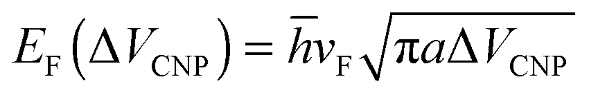
In addition to the change in PL intensity caused by the plasmonic effect, peak broadening and shift can also be observed using different contact types between metal nanomaterials and 2D semiconductors.319,320 Fang et al. examined the PL of MoS2 in hybrid nanostructures.305,321 By direct deposition of Au NPs on top of a MoS2 monolayer, a hybrid nanostructure without a spacer between Au NPs and the MoS2 monolayer was obtained. As shown in Fig. 12(a), after the Au NPs were applied to the MoS2 surface, a slight decrease in PL peaks at approximately 652 nm and 682 nm was observed. Moreover, the addition of Au NPs also resulted in the red-shifting and broadening of the MoS2 PL spectra. The main reason for this result is that if the metal NPs directly contact the 2D semiconductor, plasmon-induced hot electrons can be transferred from the metal NPs to the MoS2 by a non-radiative process, leading to the narrowing of the MoS2 band gap and a phase transition.319
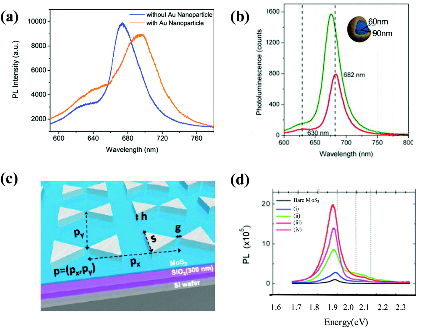 | ||
| Fig. 12 (a) PL spectrum red-shifting and broadening were found after the 5 nm diameter Au NPs were deposited on the MoS2 structure. Reproduced with permission.305 Copyright 2014, Wiley-VCH Verlag GmbH & Co. KGaA, Weinheim. (b) PL spectra of monolayer MoS2 on silica with (green) and without (red) Au nanoshells. Reproduced with permission.71 Copyright 2014, AIP Publishing LLC. The nanoshell dimensions are indicated in the inset graphic. (c) Device schematic showing the geometrical factors of a bowtie array: gap separation (g), the thickness of the metal deposition (h), the side length of a triangle (s), and unit cell dimension or pitch (p = (px, py)). (d) PL spectra of bare MoS2 (black) and four different patterns. Reproduced with permission.160 Copyright 2015, American Chemical Society. (i) s = 100 nm, p = (400 nm, 500 nm); (ii) s = 100 nm, p = (400 nm, 300 nm); (iii) s = 100 nm, p = (300 nm, 200 nm); and (iv) s = 170 nm, p = (500 nm, 800 nm). | ||
To restrain the non-radiative process, a dielectric layer can be inserted between the 2D materials and metal NPs. Recently, silica–Au–PVP (poly-4-vinylpyridine) core–shell NPs have been used to obtain a hybrid metal NP/2D semiconductor.71 Because the insulating PVP can block the electron transport between Au NPs and MoS2, the non-radiative process is effectively reduced. As a result, a PL intensity that was nearly twice as large was obtained, as shown in Fig. 12(b). To further enhance the PL intensity, a MoS2 sandwiched plasmonic coupling system consisting of an Au nanocube/PVP/MoS2/HfO2/Au film structure has also been reported.322 The PL of the MoS2 was enhanced by 2000-fold compared to the pure MoS2 for two principal reasons: (1) the dielectric PVP and HfO2 layers efficiently restrained the quenching and (2) strong plasmonic coupling was formed in the cavity between the Au nanocube and the Au film.322 Based on the principle of plasmon-enhanced PL, other dielectric materials, such as Al2O3 and small organic molecules, can also be used as insulator spacers to optimize the competition between exciton quenching and plasmonic field enhancement.274,282,283
In addition to the integration of metal NPs in 2D semiconductors,175,177 the combination of 2D semiconductors with metal nanostructures for PL enhancement has been recently reported.160 Researchers have found that both emission enhancement due to metal nanostructure scattering and absorption enhancement of the 2D semiconductor due to the localized near-field effect play important roles in enhancing the PL intensity. Agarwal et al. reported a PL enhancement in a MoS2 semiconductor with an integrated plasmonic nanoantenna array.160 As shown in Fig. 12(c), an Ag-bowtie nanoantenna array supporting SPR has been added to the top of the MoS2 monolayer. The strong exciton–plasmon coupling enables considerable light–matter interaction in the excitation and emission stages, resulting in significant PL enhancement. To demonstrate the effect of the plasmon resonance frequency in the metal nanostructures on the excitation of MoS2, the authors fabricated four patterns with different plasmonic resonance frequencies by changing the array architectures. Fig. 12(d) shows the PL spectra of a bare MoS2 and four different hybrid nanostructures, in which the PL spectrum depends strongly on the positions of the plasmonic resonance frequency. For example, the plasmonic absorption peak in the metal arrays (iii) is well-matched with the wavelength of the excitation laser; the largest PL enhancement of nearly 40-fold is achieved mainly due to the absorption enhancement excited by the localized plasmonic near-field. In addition, a maximum PL enhancement in the high-energy region occurs in the array (ii) due to strong scattering in the area shown in the array (ii), which enhances the emission of MoS2. Therefore, emission enhancement is also necessary for overall PL enhancement.
In addition to the MoS2 2D semiconductor showing a high PL in the visible region, h-BN 2D materials also exhibit a bright luminescence in the deep-violet region.258 Considering the biocompatible nature of h-BN, it is possible that this material may be used in bioimaging applications. To further enhance the PL properties of h-BN 2D materials, researchers could consider producing a plasmonic effect in the violet region. Al NPs are an excellent candidate material and show an efficient plasmonic effect in the violet region.323
In summary, the PL intensity of 2D materials with hybrid nanostructures can be enhanced by enhanced light absorption, reduced non-radiative rates, and improved emission, which enables the creation of highly efficient emitters and optical imaging devices.
4.1.1.2 PL enhancement of other species by the plasmonic effect and PL sensors based on the hybrid nanostructures. The PL enhancement of other species can also be realized. On the one hand, the optical response of outside fluorescent molecules can be directly enhanced by a metal NPs/2D semiconductor. For example, a 40-fold PL enhancement of Rhodamine B (RhB) molecules has been achieved using a graphene monolayer inserted between the RhB molecules and Ag NPs. The reason for this effect is attributed to π–π stacking interactions between graphene and the RhB fluorophore that lead to efficiently radiated emission and strong plasmonic enhancement.324
On the other hand, hybrid nanostructures of metal NPs and 2D semiconductors can be designed for efficient optical sensing by tailoring the PL of GO. GO shows intrinsic and tunable fluorescence in the red/near-infrared, visible, and ultraviolet light regions and offers exciting opportunities for nanomedicine and chemo-biosensing.326 The principle is shown in Fig. 13(a).314 GO exhibits inherent fluorescence enhancement at a particular wavelength. When the metal NPs are attached to the surface of GO, the fluorescence of GO is entirely quenched by fluorescence resonance energy transfer between GO sheets and metal NPs, which is a fundamental requirement for designing this type of sensor. However, the strong fluorescence will recover if new additives are introduced. The degree of recovery of the fluorescence of GO in the hybrid system is proportional to the concentration of the new additives, which is called “Turn-on” fluorescence detection. With this mechanism, the metal NP/2D semiconductor composite can be used as an efficient sensor to detect biomolecules and heavy metal ions.314,327 Recently, hybrid nanostructures of metal NPs/GO have been widely used as “Turn-on” fluorescence detectors325,328–330 and “Turn-off” fluorescence detectors for environmental detection and biotechnology applications.314 For example, detection of Pb2+ was reported by designing a hybrid Au/graphene system as a novel “turn-on” fluorescent sensor, as shown in Fig. 13(b).330 In this system, the PL of GO was quenched by Au NPs without the target antigen because of the fluorescence resonance energy transfer between the GO and Au NPs. After the Pb2+ was attached to the surface of hybrid nanostructures, the PL of GO was gradually enhanced depending on the Pb2+ concentration, mainly due to the GO probe quenched initially by Au NPs, which accelerated the leaching of Au NPs by the Pb2+ in the presence of both S2O32− and 2-mercaptoethanol. After measuring a series of PL intensities of the GO probes with different concentrations of Pb2+ ranging from 50–1000 nM, a linear relationship between the PL intensity and Pb2+ concentration was obtained, and the detection limit for Pb2+ was 10 nM. Moreover, a selectivity detection test was also performed by detecting other metal ions, such as Zn2+, Ca2+, Mg2+, Cd2+, Al3+, Li+, Cr3+, and Ni2+, and the intensity of the GO probes was not apparently changed, which was attributed to their weak ability to leach Au NPs. Therefore, the integration of metal nanomaterials with 2D materials can be used to produce efficient PL sensing with high detection sensitivity and selectivity.
 | ||
| Fig. 13 (a) Schematic illustration of fluorescence sensing based on fluorescence quenching of GO by decorating Au NPs and enhancement by the leaching of Au NPs. Reproduced with permission.314 Copyright 2014, American Chemical Society. (b) Fluorescence spectra of G–Au NCs in 5 mM glycine solution upon the addition of increasing concentrations of Pb2+ ions (0 M–1000 nM) under optimal conditions.330 Copyright 2012, American Chemical Society. | ||
4.1.2.1 Hybrid nanostructures as SERS substrates for detection of target molecules. Great achievements have been made in the design and fabrication of hybrid nanostructured SERS substrates. Initially, hybrid metal/graphene systems that were used as SERS substrates were fabricated using thermal evaporation of Ag nanospheres on top of CVD grown graphene.278 SERS experiments demonstrated that the hybrid device showed a stronger SERS enhancement than that of single Ag nanospheres or the graphene SERS substrate.79,343,344 Because the morphology of metal NPs strongly affects SERS signals, other shaped metal NPs have also been added to the graphene surfaces of hybrid SERS substrates.345 Au nanorods with graphene or GO have shown to significantly enhance the SERS signal of crystal violet (CV) and allow the detection of pesticides with a limit of detection of approximately 5 × 10⁻⁷ M.346,347 The Raman signals of nitro explosives can be enhanced by four orders of magnitude when a GO–Au nanocage hybrid platform is applied.348 In addition, Au nanohexagons on graphene and a cooperative graphene–Au nanopyramid system have also been reported as excellent SERS substrates.349,350
In addition to simple combinations of metal NPs with graphene used as hybrid SERS substrates, some unique hybrid nanostructures have been reported recently. Because molecules directly absorbed on the plasmonic metal surface will induce unfavorable disturbances including chemical adsorption-induced vibrations, charge transfer between the metal and molecules, photo-induced damage, and metal-catalyzed side reactions, researchers have attempted to use an ultrathin layer of 2D materials as an inert shell.159,351 Zhang et al. placed CVD-grown graphene on top of a tightly packed Au nanosphere film and demonstrated an active, graphene-veiled plasmonic metal SERS substrate.159 Tian et al. also reported graphene shell isolated metal NP enhanced Raman scattering.352 In addition, metal NPs added to vertical graphene sheets have been used as a 3D SERS substrate with high reproducibility.77 Recently, a sandwiched metal NP/graphene/metal film hybrid system has received increased attention due to its promise of being used in SERS applications.284,297,303,353–356 As shown in Fig. 14(a), the sandwiched hybrid structure is composed of Ag NPs with a diameter of 20 nm residing on an ultrathin graphene spacer layer covering an Ag film.63 Due to the 2D nature of graphene, very strong plasmonic coupling was achieved via the sub-nanometer gap between the upper metal NPs and the lower metal film. In addition, the increased ability of graphene to absorb and concentrate target molecules further makes it an attractive candidate for SERS applications (Fig. 14(b)).63 Because Au and Ag materials are rare and expensive, researchers have attempted to find other less expensive metal materials to use them as efficient SERS substrates. Cu NPs are a promising SERS substrate and are widely used in biotechnology. However, the enhancement factor (EF) of Cu NPs is only 1.57 × 10⁴, which is considerably lower than that of Au and Ag NPs. Our group has proposed the construction of a Cu NP/graphene/Cu film coupling system by directly evaporating Cu NPs on top of graphene grown on a Cu foil.89 Using two strategies, including the coupling between Cu NPs and Cu film and the use of optimized incident light to enhance the vertical component of the electrical field in the interaction with the Cu-NP image, one of the highest EF values (1.89 × 10⁷) for the Cu SERS substrates has been achieved (Fig. 14(c) and (d)).
 | ||
| Fig. 14 (a) The 3-dimensional and cross-sectional schematic of graphene sandwiched with an Ag coupling system as a strong SERS substrate and (b) the impressive features of the SERS substrate possess a strong near-field due to NP-film coupling and a chemical mechanism enhancement from the monolayer graphene sub-nanospacer through interacting with target analytes owing to a strong π–π interaction. Reproduced with permission.63 Copyright 2014, Wiley-VCH Verlag GmbH & Co. KGaA, Weinheim. CuPc Raman spectra detected on the Cu NPs/graphene/Cu film coupling system (Cu–NGF–6NPs) with the incident light (c) at 0 deg. and (d) at 60 deg. Reproduced with permission.89 Copyright 2015, Royal Society of Chemistry. “∇” denotes the Raman signals from the monolayer graphene in the Cu–NGF system. The excitation wavelength is 532 nm. The accumulated time is 20 s, and the laser power is 5 mW. | ||
In addition to graphene and GO, which are popularly reported to combine with metal NPs and create excellent SERS substrates, hybrid nanostructures of metal NPs with other 2D materials (i.e., h-BN, MoS2) have recently been reported.121,126,130,155,357–359 However, the hybrid nanostructures reported to date involve the straightforward combination of metal NPs with an h-BN or MoS2 monolayer. More unique and complicated hybrid nanostructures with stronger interactions between metal NPs and h-BN and MoS2 need to be further developed.
4.1.2.2 Hybrid nanostructures as SERS tools to study other physical phenomena. First, hybrid nanostructures can be used to evaluate plasmonic near-field enhancement using the SERS technique because SERS enhancement is strongly related to its plasmonic near-field enhancement in plasmonic nanostructures. Because graphene and other 2D materials have well-known Raman spectra, they function as appropriate test materials for investigating the plasmonic effects of hybrid systems. Reich et al. demonstrated the strong near-field coupling in a hotspot between two Au nanodisks using Raman scattering of graphene (Fig. 15(a)).166 Because near-field enhancement is hard to evaluate directly, they introduced a monolayer of graphene on top of an Au nanodisk dimer to study the coupling between the two Au nanodisks.
 | ||
| Fig. 15 (a) Schematic description of monolayer graphene covered on two Au nanorods, and (b) the Raman spectra of graphene obtained from graphene with (red line) or without (black line) plasmonic enhancement. Reproduced with permission.166 Copyright 2012, American Chemical Society. (c) Schematic description of detecting strain using the plasmonic effect, and (d) the corresponding Raman spectra of MoS2 with (red line) or without (black line) applying strain. Reproduced with permission.360 Copyright 2014, American Chemical Society. | ||
As shown in Fig. 15(b), the Raman intensity of graphene was significantly enhanced after the Au nanodisk dimer was applied, which indirectly reflects the strong near-field coupling between the two Au nanodisks. We also used the Raman spectrum of graphene to explain the strong plasmonic coupling between the upper Cu NPs and lower Cu film when graphene was used as a nanospacer.112 It is important to note that a very recent report showed that quantum mechanical effects will emerge if the thickness between the upper metal NPs and the lower metal film approaches the atomic length scale in metal NP/metal film coupling systems.361–364 Thus, it is imperative to determine if a quantum effect exists in the NP/graphene/film hybrid system in the future when the SERS technique is used to study the plasmonic effects.
The powerful plasmonic enhancement can also be used to observe fine Raman bands that are not observed using normal Raman spectra. Recently, Baumberg et al. probed confined phonon modes using the SERS technique in CdSe nanoplatelets sandwiched between Au NPs and an Au film.61 In addition, the hybrid nanostructure of an SERS substrate can also be used to monitor morphological changes in a 2D monolayer.365 The Raman spectrum of a material with vibration information is its fingerprint. When the material morphology changes, its Raman spectrum also varies. However, a challenge remains in collecting Raman information from some nanomaterials such as MoS2 without the assistance of the plasmonic effect. Tiny variations in morphology are particularly difficult to observe. Using a MoS2 layer sandwiched with a strong plasmonic coupling between the metal NPs and the metal film, the morphological changes in the middle MoS2 layer have been well studied.365 Moreover, local strain in the hybrid nanostructures can also be detected using the SERS technique because the Raman spectra of materials are strongly affected by the local stress. Wang et al. found that the hybrid nanostructures of SERS substrates can be used to probe the local strain at MoS2 film/Ag NP boundaries.360Fig. 15(c) shows a schematic description of the strain detection using the plasmonic effect.360 When Ag NPs are placed on top of the MoS2 surface, local strain occurs near the MoS2/Au NP boundaries. As a result, the Raman spectra of MoS2 that undergoes local strain are changed, and the minimum change in the Raman spectra can be greatly amplified (Fig. 15(d)). Based on the change, the local strain can be evaluated. In conclusion, any physical phenomenon in hybrid metal/2D material systems that affects the Raman spectra of 2D materials, such as the plasmonic near-field, morphological changes, and local strain, can be studied using the SERS technique.
An SPR sensor composed of a hybrid metal/2D material system has a typical structure of prism/metal film/2D materials/host molecules, as shown in Fig. 16(a).179 Host molecules are added to the sensor to trap the analytes of interest, resulting in sensitive detection and efficient selection. A Kretschmann configuration can be used to excite surface plasmon-polariton on the 2D material–Au surface.72,315,317 The following equation is used:
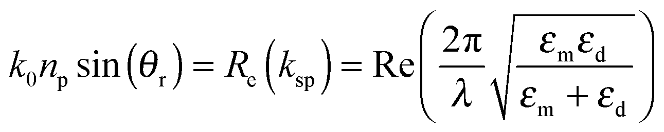 | (13) |
 | ||
| Fig. 16 (a) Schematic diagram of a graphene–MoS2 enhanced SPR biosensor. Reproduced with permission.179 Copyright 2015, Elsevier B.V. (b) The SPR angle shifts after anti-CT injection using pure Au (red) and graphene–Au (black) surfaces functionalized with polypyrrole–NTA/Cu2+/b-CT at two different anti-CT concentrations (a and b: 4 ng mL−1 and c and d: 35 ng mL−1), and (c) linear range of the graphene-based SPR immunosensor toward anti-CT. Reproduced with permission.370 Copyright 2015, American Chemical Society. | ||
Based on recent studies, two key principles should be considered when designing a sensitive SPR sensor. The first is to create a hybrid nanostructure that shows a keen sensitivity to the refractive index of the environment. The second is to add host molecules to the hybrid nanostructures that have a strong selectivity for the analytes of interest. Among the hybrid nanostructures of metal/2D materials that function as SPR sensors, graphene covering a metal surface is a typical example.317,370,371 Cosnier et al. reported the construction of an SPR immunosensor by adding a monolayer of graphene to an Au film.370 Graphene was noncovalently functionalized using nitrilotriacetic acid (NTA) with polypyrrole and the pyrene groups and biotinylated cholera toxin (b-CT) as a receptor to detect the anti-cholera toxin in rabbits (anti-CT). As shown in Fig. 16(b), the SPR angle shifts after anti-CT introduction using pure Au (red) and graphene–Au (black) with NTA on the surface at two different anti-CT concentrations. At the same anti-CT concentration, the introduction of the graphene monolayer enhances the detection sensitivity by approximately 2-fold. In addition, the SPR angle of the graphene/Au hybrid nanostructures is increased along with the anti-CT concentration from 4 ng mL−1 to 35 ng mL−1. The SPR response was recorded by plotting the SPR angle and the anti-CT concentration after 50 s, and a linear relationship was obtained between the SPR angle and the anti-CT concentration between 0.004 and 4 ng mL−1 with a lower limit of detection (LOD) of approximately 4 pg mL−1 (Fig. 16(c)). To further enhance the sensitivity of the sensors, more than one type of 2D material has been integrated to utilize their collective advantages.179 It has recently been reported that a phase-sensitivity enhancement factor of more than 500-fold was obtained in the proposed hybrid nanostructures of metal film/graphene–MoS2 2D materials compared to the SPR sensing design without graphene–MoS2 or with only graphene introduction.179 Compared to other detection methods, such as amperometry or photoelectrochemical transduction, the SPR sensor based on the hybrid nanostructures of metal/2D materials has a lower LOD, implying promise for chemical and biological sensing applications in the future.370
4.2 Plasmon-enhanced catalytic reactions
A solar-driven photocatalytic reaction based on electron–hole pair generation in semiconductors is an economical and practical solution for green and renewable energy and has attracted an extensive interest in recent years. Many reports and reviews have been published regarding plasmon-enhanced catalytic reactions performed by utilizing the hybrid nanostructures of metal NP/inorganic semiconductor photocatalysts, especially for metal NP/metal oxide semiconductors hybrids (i.e., TiO2 and ZnO).70 Recently, the incorporation of plasmonic metal NPs in 2D semiconductors (i.e., GO, MoS2) has resulted in the improved performance of high-efficiency photocatalysis.372 Here, we will mainly focus on the plasmonic effect in the hybrid nanostructures of plasmonic metal/2D semiconductors and discuss their principles and applications in the photodegradation of organic pollutants and photocatalytic production of hydrogen. | ||
| Fig. 17 Schematic illustration of the mechanisms for plasmon-enhanced chemical reactions with metal/semiconductor hybrid nanostructures. Reproduced with permission.70 Copyright 2014, Wiley-VCH Verlag GmbH & Co. KGaA, Weinheim. (a) Plasmonic absorption enhancement. (b) Hot-electron effect. (c and d) Processes involved in the hot-electron effect. CB and VB represent the conduction and valence bands of the semiconductor, respectively. EF refers to the Fermi energy level. | ||
The second confirmed mechanism for plasmon-enhanced chemical reactions is electron transfer.62 Upon plasmonic excitation, the electron transfer process from the metal to the semiconductor occurs at the metal/semiconductor interface (Fig. 17(b)).70 In general, the Fermi level of a 2D semiconductor is different from that of metal Au or Ag nanomaterials. Thus, a Schottky barrier forms at the junction interface between the metal and the semiconductor in the hybrid nanostructures, which blocks the electron transfer from the metal to the semiconductor. However, with the strong plasmonic excitation induced by the metal NPs, the hot electrons can transfer from the metal to the conduction band of the semiconductor. During this process, the plasmon quantum with the highest electron energy can decay non-radiatively into an electron/hole pair.373 The decay rate depends on the size of the metal NPs and the radiative behavior of the plasmonic mode. In general, subradiant plasmon modes or small metal NPs can quickly generate electron/hole pairs. As shown in Fig. 17(c), the electron/hole pair is created when an electron is excited by the plasmon quantum from the Fermi level to an unoccupied state. Subsequently, coherence in the excited hot electron is lost, and a non-equilibrium Fermi–Dirac-type distribution is followed (Fig. 17(d)).70 If photogenerated hot electrons have sufficient energies to overcome the Schottky barrier formed between the metal NPs and the semiconductor, they can successfully transfer to the CB of the semiconductor. As a result, even if a semiconductor has a weak ability to absorb light in the visible region, it obtains additional electrons from the metal NPs and thus conducts chemical reactions.374,375 In addition, the holes remaining in the metal NPs show a slight oxidation ability and can be used for chemoselective oxidation reactions.376,377
The third possible mechanism is the scattering mechanism.378 Metal NPs with sizes larger than 50 nm can efficiently scatter the resonant photons. Using this channel, the path length of photons near the semiconductors can be increased, thus enhancing the light absorption of the semiconductors. In addition to the large size, which is preferable for scattering, the shape and loading level of metal NPs in the hybrid metal NPs/2D semiconductor system also strongly influences scattering. Compared to the metal nanospheres, metal nanocubes, which have more edges and corners, show more efficient optical scattering. Excessively low or high loading of metal NPs is not beneficial for maximum light scattering.
In summary, the configurations of the hybrid metal/semiconductor systems and detailed arrangements of the two single components determine which mechanism is dominant in a particular photocatalytic reaction.70,378 Plasmon-induced hot electron transfer occurs when the electrons in metal NPs are excited above the CB of the semiconductor. Close contact between the metal NPs and semiconductors is necessary for electron transfer. If a non-conductive spacer is inserted between the metal NPs and semiconductor, the scattering mechanism and the near-field enhancement are dominant. A stronger scattering can be achieved in the hybrid system if multiple scattering of resonant photons is obtained via the optical arrangement. In addition, the detailed arrangement of metal NPs and a semiconductor strongly affects the generation and separation of electron and hole pairs after plasmonic near-field enhanced absorption is achieved. Therefore, a rational study is required for the design of a hybrid metal/semiconductor system that exploits the maximum advantage of these mechanisms.
A simple hybrid nanostructure produced by directly adding Au NPs onto GO materials has shown excellent performance in the photocatalytic degradation of RhB dyes under visible light.80 The RhB degradation rate was markedly increased under visible light irradiation after the introduction of metal NPs into GO. The authors attributed the deterioration of the dye pollutants to the reactive oxidative species produced by the Au NP/GO hybrid system under visible light irradiation. However, the roles of Au NPs in plasmon-assisted light absorption have not been discussed. Considering that the metal NPs are energetically unstable, tend to aggregate during the catalytic reaction, Su et al. fabricated Au NPs embedded into a hollow graphene nanoshell to avoid the aggregation of NPs efficiently and show robust catalytic performance.379
Relatively complex hybrid nanostructures have also been fabricated for visible-light photodegradation of organic pollutants.60,380 Jin et al. reported a new photocatalyst with graphene-supported CdSe/CdS quantum dot (QDs)/Au NP hybrid nanostructures (QDs/Au–G).60 Two types of photocatalysts exist including semiconductor GO and semiconductor QDs. As illustrated in Fig. 18(a), electrons are excited from the VBs to the CBs of the QD and GO semiconductors under visible-light irradiation. Meanwhile, the Au NPs can form a localized near-field to enhance light absorption in the visible region and increase the electron–hole pair generation rate at the surface of the semiconductors, and then the electrons are transferred into satellite Au NPs. The optical properties of QDs with or without Au NPs can be demonstrated using UV-vis and PL spectra (Fig. 18(b) and (c)). Before Au NPs are attached to the QDs, optical absorption consists of a broad wavelength range with a clear peak at 620 nm. In addition, a narrow PL peak of approximately 640 nm is clearly observed, as shown in Fig. 18(b). After the formation of a hybrid nanostructure of Au NPs and QDs, the intensity of the optical absorption is significantly increased compared to that of pure QDs with the same concentration (Fig. 18(c)). The absorption range also extends to longer wavelengths. Moreover, the dark field scattering image of the QD/Au system is obviously colored, compared to that of the QD system without Au NPs, which directly reflects the plasmonic enhancement of Au NPs on the QD semiconductor. The efficient electron transfer from QDS to Au NPs can be demonstrated by a pronounced decrease in PL after Au NPs are introduced into QDs. Furthermore, a visible-light photocatalytic reaction using QD/Au–G has been shown (Fig. 18(d)). Compared to the QD–G composite, the QD/Au–G hybrid nanostructure exhibits a more efficient photocatalytic performance. After 1 h of irradiation with visible light, 65% of the original MB was decomposed when photocatalyzed by QD–G. In contrast, nearly 80% of the original MB can be decomposed using the QD/Au–G hybrid nanostructure, which further confirms that light absorption can be enhanced with Au NPs. If the QDs, Au, and GO nanomaterials are simply blended as a photocatalyst (QDs–Au–G), only 50% of the original MB can be decomposed, which demonstrates that the Au NPs arrangement is also critical for utilizing the plasmonic effect.
 | ||
| Fig. 18 (a) The charge separation and transfer processes of the graphene-supported CdSe/CdS quantum dots (QDs)/Au NPs system by the localized plasmonic effect. The UV-vis (black), PL (red) spectra, and dark-field scattering images (inset) of the (b) CdSe/CdS QDs, and (c) CdSe/CdS–Au system. In the (c), the black dotted line refers to CdSe/CdS, and the solid black lines refer to CdSe/CdS/Au. (d) Photodegradation of methylene blue (2.7 × 10⁻⁵ M, 10 mL) under visible light (>420 nm) over QDs/Au–G, QD–G, and QD–Au–G photocatalysts (3 mg), respectively. Reproduced with permission.60 Copyright 2014, American Chemical Society. | ||
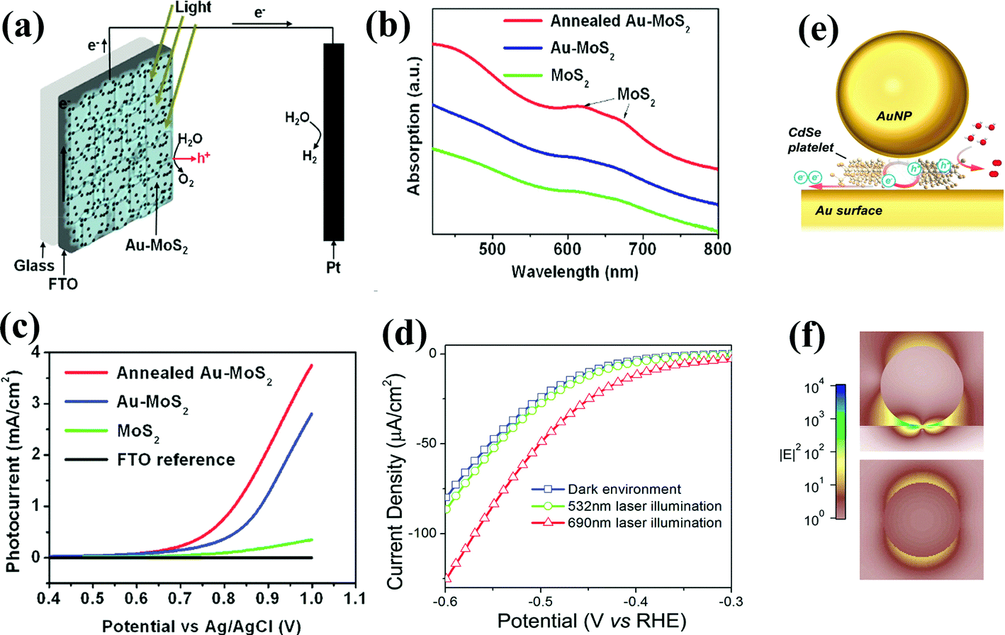 | ||
| Fig. 19 (a) Schematic representation of PEC with Au/MoS2 on FTO and commercial Pt wire as a photoanode and a photocathode, respectively. (b) UV spectra of MoS2, Au/MoS2, and annealed Au/MoS2. Arrows point to the absorption peaks of MoS2, and (c) linear sweep voltammograms for PECs with different working electrodes. Reproduced with permission.383 Copyright 2014, Wiley-VCH Verlag GmbH & Co. KGaA, Weinheim. (d) The polarization curves of the hydrogen evolution reaction in the dark environment, 532 nm and 690 nm laser illumination. Reproduced with permission.319 Copyright 2015, Royal Society of Chemistry. (e) Au NPs on Au film with atomically thin CdSe sandwiched between them, and (f) field enhancement at the optical bandgap of the CdSe platelets (λ = 548 nm) in the coupling-nanogap (top) and for an isolated AuNP (bottom) for comparison. Reproduced with permission.61 Copyright 2015, American Chemical Society. | ||
The introduction of Au NPs into the GO materials produces better performance in the production of hydrogen via the absorption enhancement of the GO/QD semiconductor and the increase in the electron–hole pair generation rate at the surface of the GO semiconductor.60 In addition, an Au–MoS2 composite is another plasmon-enhanced photocatalyst that produces efficient water-splitting in a photoelectrochemical cell (PEC).383,385Fig. 19(b) shows the absorption spectra of MoS2, Au–MoS2, and annealed Au–MoS2. Compared to pure MoS2, Au–MoS2 shows two absorption peaks near ∼620 and 670 nm, which are mainly due to plasmon-enhanced absorption. After applying the annealing treatment at 350 °C for 1 h in Ar, the semiconducting phase of the prepared MoS2 is enhanced, and the interface resistance between the MoS2 and Au NPs is reduced. As a result, the absorption intensity of the Au–MoS2 composite is further improved, as shown in Fig. 19(b). The linear sweep voltammograms are shown in Fig. 19(c). Under visible light irradiation, the photocurrent increases from 100 μA cm−2 at 0.8 V for pure MoS2 nanosheet-based PEC to 370 μA cm−2 after 3 wt% Au NPs are loaded on the MoS2 nanosheet without the annealing process. Furthermore, the photocurrent is further increased to 790 μA cm−2 after Au–MoS2 is annealed. Another method used to confirm that the plasmonic near-field effect plays a significant role in enhancing the light absorption is to tailor the wavelength of incident light.319 As shown in Fig. 19(d), the measured current density increases from ∼75 to ∼125 μA cm−2 when the irradiated light wavelength is changed from off-resonance excitation at 532 nm to resonance excitation at 690 nm, which strongly reflects the important role of plasmon-enhanced absorption in enhancing the photocatalytic reaction.
In addition, complicated hybrid nanostructures have been proposed to enhance the photocatalytic performance efficiently. A sandwiched CdSe nanoplatelet has been constructed by inserting the ultrathin CdSe nanoplatelet between metal NPs and a metal film, which shows an enhanced water-splitting activity due to the excited plasmonic coupling between the metal NPs and the metal film (Fig. 19(e)).61 Because the thickness of the CdSe nanoplatelet is only several nanometers, a strong plasmonic coupling throughout the CdSe material results in dramatically higher electromagnetic field enhancements in the complicated Au NPs/CdSe/Au film nanostructures compared to the simple hybrid nanostructure (i.e., Au NPs/CdSe) (Fig. 19(f)). As a result, the Au NPs/CdSe/Au film photocatalytic nanostructure shows a 5-fold increase in the photocurrent, while the hybrid nanostructure of Au NPs/CdSe displays only a two-fold increase compared to the pure CdSe semiconductor. Considering the poor stability of MoS2 and CdSe,61,365 other semiconductors with better stability should be considered in future designs for water splitting.
After discussing recent reports of plasmon-enhanced catalytic reactions, a summary is presented. First, metal nanomaterials play a significant role in enhancing optical absorption in the visible region. Metal nanomaterials also produce many positive electrical effects, such as improving photogenerated electron transfer, facilitating exciton separation, and providing plasmonic “hot electrons”.289,373 Two important issues should be considered when developing high-performance plasmon-enhanced photocatalysts. (1) Typical metal NPs have a relatively narrow plasmonic resonance, which enhances light absorption in a small region. For efficient utilization of sunlight, which is a broadband light source, hybrid nanostructures of metal nanomaterials/2D materials with broadband plasmonic absorption enhancement should be designed. (2) The photogeneration rate should be significantly enhanced, and recombination of charge carriers should be further reduced by fabricating high-quality 2D materials, carefully arranging metal components and 2D materials in the hybrid nanostructures, and modifying the interface between the metal nanomaterials and 2D materials.
4.3 Optoelectronics
Optoelectronics is a cross-discipline of photonics and electronics that revolves around the mutual conversion of light and electronics in semiconductor devices. According to the different functions and evaluation criteria, optoelectronic devices can be divided into photovoltaic cells (PVs), photodetectors (PDs), and light emitting diodes (LEDs), among others. 2D materials have a broad range of applications in optoelectronic devices due to their unique structures and optical properties.6,9,14,16,17,25,383,386,387 First, a graphene layer can be employed as a highly transparent electrode in photoelectronic devices, including any PV, PD, and LED, due to its high conductivity.1,15 Second, the energy bandgap tunability of 2D materials, such as GO and MoS2, enables them to act as work-function tunable interlayers in PVs and LEDs.184 In addition, graphene, GO, and TMDs display variable levels of photon absorption, allowing them to be utilized as photoactive materials in optoelectronic devices, especially photosensitive PDs, which have been reported recently.24,35,184,386,388 An apparent reason to integrate metal NPs with 2D materials into hybrid nanostructures is to enhance the light absorption of 2D materials through the plasmonic light-trapping effect.40 In addition, plasmon-induced hot-electron generation at metal component/2D material interfaces plays a significant role in photovoltaic devices.62 Moreover, because 2D materials have a flat surface with a large area, they are very promising building blocks for devices. The comprehensive configuration and detailed arrangement of metal components and 2D materials used in hybrid systems have a strong influence on the functions of the devices and their applications.12,81,389 In this section, we will mainly discuss two typical applications in optoelectronics for hybrid nanostructures of metal/2D materials, PVs and PDs.Hybrid nanostructures of metal nanomaterials and graphene can be used as flexible and transparent electrodes in solar cells.380 Initially, graphene was used to replace the fragile ITO due to its excellent electrical and mechanical properties.188,390,391 However, monolayer graphene has low electrical conductivity (sheet resistance Rs > 1000 Ω sq−1) and does not perform well as a working electrode due to defects and disruptions such as wrinkles and folding.391,392 To solve this problem, metal nanomaterials can be integrated with the graphene to form composite electrodes.392–398 In addition to the improved electrical conductivity of electrodes, the introduction of metal nanomaterials has other positive effects on the electrodes, including enhanced light absorption of devices and tunable working functions of the electrodes.399 A typical example of a hybrid electrode consisting of a metal nanomaterial/graphene is made by placing Ag nanowires on top of a graphene monolayer. As a result, the Rs is decreased from 1050 to 64 Ω sq−1 after the Ag nanowires are applied, and the transmittance is nearly unchanged (94%).382 Considering that Cu is relatively cheaper than Au and Ag, Cu nanowires have been used to replace Ag nanowires.382 In addition, metal nanospheres can also be used to reduce the resistance of the electrode. Chen et al. selectively filled Au NPs in the cracks in a graphene film. The crack-filled graphene film (CFG) with Au NPs showed excellent electrical properties as a transparent electrode and produced a 30% enhancement of the power conversion efficiency (PCE) in graphene/Si Schottky solar cells.400 Wang et al. also improved the efficiency of graphene–silicon Schottky solar cells by introducing Au NPs on top of a graphene electrode and attributed the remarkable improvement of device efficiency to the increased work function and improved electrical conductivity.401 However, the optical effect of Au NPs on the device was unfortunately not addressed in the study. Due to the large dielectric index of silicon, light trapping is possible. Further measurements of the absorption of devices with or without Au NPs should be performed in future studies.
The hybrid nanostructures of metal/2D semiconductors can be used as an interlayer of photovoltaic cells. Solution-processed metal oxides and other semiconductors have been used as interlayers in thin-film solar cells. For instance, solution-processed GOs and MoS2 have been reported to be alternatives to poly(3,4-ethylenedioxythiophene)–poly(styrenesulfonate) (PEDOT:PSS) in the hole transport layer (HTL).229,236,244,246,402–407 However, the problem of absorbing sufficient light using thin-film solar cells, especially OSCs, is a current challenge. Among the techniques developed for light trapping, exploiting the plasmonic effect of metal NPs has been shown to be an efficient strategy.190,408,409 The integration of metal NPs with 2D materials as hybrid nanostructures has been used not only to produce a solution-processed interlayer but also as an effective light-trapping strategy, via the plasmonic near-field effect and scattering effect, to enhance the absorption of solar cells.389,402 In addition, metal NPs can produce positive electronic effects, including enhancement of electrical conductivity, increases in the exciton generation rate, and improvement of carrier collection.
As shown in Fig. 20(a), the HTL of the control device is the PEDOT:PSS. To enhance the device performance, a hybrid Ag NPs/GO layer has been introduced into the PEDOT:PSS as a composite HTL in the OSCs.402 As a result, the Jsc and PCE are improved from 8.47 mA cm−2 and 3.23% for the reference to 9.43 mA cm−2 and 3.55% for the device with the Au/GO interlayer, respectively (Fig. 20(b)).402 The increased Jsc with the Au/GO interlayer is mainly due to the strong plasmonic effect of Ag NPs, which improves light absorption. As shown in Fig. 20(c), the trend of absorption enhancement is consistent with the pattern of monochromatic incident photon-to-electron conversion efficiency (IPCE) improvement, which implies that the Jsc increment is due to improved absorption.402 The strong light-trapping effect of the Au NPs can also be illustrated by the theoretical near-field curve (Fig. 20(d)).402 Under illumination with the incident light near the LSPR of Au NPs, a high electric field distributed near the Au NPs is observed. In addition, after the Au/GO hybrid is applied to the interlayer, the exciton generation rates of the devices are also significantly improved, which has been demonstrated using the steady state and dynamic photoluminescence measurements. Moreover, hybrid nanostructures consisting of metal NPs/MoS2 have also been demonstrated as efficient HTLs.81Fig. 20(e) describes solar cells with an ITO/MoS2 or MoS2/Au HTL/active layer/electron transport layer/Al structure. The device parameters, including Jsc, FF, and PCE, are significantly enhanced from 13.36 mA cm−2, 0.634, and 6.18% for the control device with only MoS2 as an interlayer to 15.44 mA cm−2, 0.652, and 7.25% for the device with the Au (12.5 wt%)/MoS2 hybrid used as the interlayer (Fig. 20(f)). It is important to state that the device performance of solar cells is very sensitive to the Au concentration incorporated in the HTL. A high concentration (e.g., 20 wt%) may lead to a device short, and a low level (e.g., 2.5 wt%) produces negligible optical and electrical effects on the device. Using the optimized Au NPs/MoS2 hybrid, the light absorption, photogeneration rate, and carrier collection were all well enhanced. Because h-BN as an insulator cannot be used in solar cells, few studies have reported the use of a hybrid of metal NPs/h-BN materials in solar cells to date.
 | ||
| Fig. 20 (a) Schematic of organic solar cells with the structure of ITO/Au–GO or GO/P3HT:PCBM/LiF/Al, (b) J–V characteristics of polymer solar cells with and without GO or Au–GOs in the PEDOT:PSS layer recorded under AM 1.5 G simulated solar illumination at 100 mW cm−2, (c) comparison of the differences in IPCE (ΔIPCE) after incorporating Au–GOs, and the absorption spectra of Au–GO, and (d) simulated light intensity (|E|2) distribution around isolated Au NPs with the diameter of 6 nm in PEDOT:PSS at the plasmonic resonance position of 650 nm. Reproduced with permission.402 Copyright 2012, Royal Society of Chemistry. (e) Chemical structures of PTB7 and PC71BM and a schematic of the device architecture with the structure of ITO/MoS2@Au/BHJ/PFN/Al, and (f) the corresponding J–V characteristics. Reproduced with permission.81 Copyright 2014, Royal Society of Chemistry. | ||
2D materials can also be used as active layers. GO synthesized using chemical methods can be used to replace [6,6]-phenyl C61 butyric acid methyl ester (PCBM) in organic solar cells.272 By blending the GO with poly(3-hexyl)thiophene (P3HT) and using it as an active layer, the OSC produces distinct photogenerated current. Other 2D materials have also been used as active layers of solar cells, such as MoS2,410 and WS2.411–413
Graphene is the first channel material utilized in back-gate type PDs. However, as discussed in Section 3.2, the intrinsically weak light absorption (∼2.3% for pristine graphene) and its short photocarrier lifetime lead to poor photoresponsivity (5 × 10⁻⁴ AW−1) and internal quantum efficiency (6–16%). An efficient method to enhance light absorption is to utilize the near-field enhancement from the excitation of the plasmonic effect induced by the metal nanostructures. By placing the plasmonic nanostructures close to the graphene, the photoresponse of graphene-based PDs can be efficiently improved.161–163Fig. 21(a) shows the layout of a graphene-based PD.163 The graphene monolayer is transferred onto a silicon substrate covered with a 250 nm silica film, followed by placing the metal nanomaterials on top of the graphene monolayer. Then, Ti/Au electrodes are fabricated on graphene using EBL and act as source and drain electrodes, and the silicon substrate is the gate electrode. After the metal nanostructures are introduced, the photocurrent and external quantum efficiency of the hybrid device show a 15-fold enhancement compared to the graphene-based PD (Fig. 21(b)).163 The photocurrent is attributed to plasmon-enhanced primary carrier excitation of graphene electrons and plasmon-induced hot electron transfer from the metal nanostructures into the graphene nanosheet (Fig. 21(d)). In addition, plasmonic nanostructures with a variable resonance can be used to amplify the photoresponse of graphene selectively to light at the desired wavelength, enabling highly accurate photodetection.178 Besides the plasmonic effect, which affects the photocurrent of PDs, applied gate voltage also changes the photocurrent. Recently, a sandwiched plasmonic nanoantenna between two single graphene layers was designed as a graphene-based light-concentrating PD.178 As shown in Fig. 21(c), the photocurrent near the scanning position (e.g., −4 μm) can be efficiently enhanced to 80, 100, and 125 nA after the gate voltage is increased from 0, −20, or −40 V.
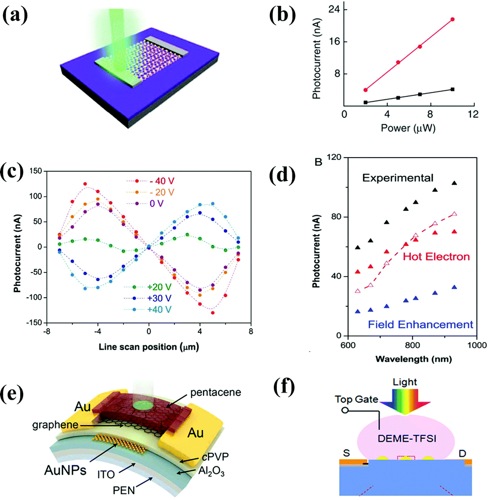 | ||
| Fig. 21 (a) Schematic of a nonamer antenna on single-layered graphene with back-gated voltage and source and drain contacts, and (b) photocurrent generated as a function of laser power. Reproduced with permission.163 Copyright 2011, Nature Publishing Group. The red and black lines indicate the response of a typical device with and without Au nanoparticles, respectively. The laser wavelength is 514 nm. (c) Measured photocurrent for gate bias voltage between −40 to +40 V for the plasmonic antenna-patterned device with the incident laser power of 10 μW, and (d) measured photocurrent and calculated photocurrent. Reproduced with permission.178 Copyright 2012, American Chemical Society. (e) Schematic diagram of the device structure comprising a graphene photodetector with a pentacene light absorption layer and an AuNP charge trapping layer. Reproduced with permission.64 Copyright 2015, American Chemical Society. In the device, the ITO acts as a gate electrode and Au as a source/drain electrode. (f) Schematic of the Ag NP/graphene hybrid FET photodetector with possible cation distribution changes around an Ag NP through LSPR generated Ohmic heating and/or direct energy transfer. Reproduced with permission.414 Copyright 2014, Wiley-VCH Verlag GmbH & Co. KGaA, Weinheim. | ||
A new multifunctional graphene optoelectronic device can be designed by introducing additional semiconductors into the graphene-based PDs.64 As shown in Fig. 21(e), the organic semiconductor pentacene, Au NPs, and graphene can be combined to fabricate a photodetecting device with a nonvolatile memory function for storing photonic signals. Pentacene acts as a light absorption layer in the device and provides a high photocurrent to the graphene channel. Au NPs, positioned between the tunneling and blocking dielectric layers, act as both a charge trap layer and a plasmonic light scatterer, which enable the storage of the incident light information. The proposed pentacene–graphene–AuNP hybrid photodetector not only performs well as a PD in the visible light range but also stores the photonic signal in the form of persistent current. The good photodetection performance of the device results from the plasmonic enhancement of the optical absorption and the photogating mechanisms in pentacene. The photodetector provides a photoresponse that depends on the wavelength of incident light; therefore, the signal information (both the wavelength and intensity) of the incident light is effectively committed to memory. The simple process of applying a negative pulse gate voltage can erase the programmed information.
In addition to the back-gate type PDs, hybrid nanostructures of metal nanomaterials/graphene applied to ionic liquid gated graphene FETs reveal a double-layer capacitance, which is 9.2–21 μF cm−2, approximately 2–3 orders of magnitude higher than the back-gate capacitance using a layer of 90 nm SiO2 (approximately 38 nF cm−2).417 Wu et al. have proposed a high-performance PD based on an ionic liquid gated plasmonic Ag NP/graphene nanohybrid FET, which takes full advantage of plasmon-enhanced light trapping by the metal nanostructures in addition to the high gating efficiency of the ionic liquid on graphene FET channel conductivity (Fig. 21(f)).414
Other 2D materials such as MoS2 materials can also be used as channel materials.418 Compared to the advantages of graphene, such as offering broadband detection and ultrafast sensitivity, the MoS2 monolayer has attracted much interest due to its potential for achieving a very high responsivity of 7.5 × 10⁻³ AW−1via the application of a back-gate voltage (Vg) of 50 V.254 Moreover, by adjusting the number of layers in TMDC crystals, intriguing optical properties, such as an indirect to direct band gap transition, an increase in band gap energy (Eg), Van Hove singularities in the electronic density of states, and valley polarization, have been discovered in TMDCs (MoS2, MoSe2, WS2, and WSe2), which are essential for realization of highly efficient and advanced optoelectronic devices.4 Similarly, the amount of light absorbed by such thin MoS2 nanomaterials cannot satisfy practical requirements. To address the issue, metal nanostructures have been introduced into TMD based PDs. The active plasmonic effect in metal nanostructures primarily improves the light absorption in the cross section of the underlying MoS2 layer and naturally increase the photocurrent of PDs.419,420 Regarding other materials in the 2D material family, optoelectronic applications are still in their early stages of exploration, and new findings in PD performance, as well as the diversity of the spectral range, can be anticipated.253,421–424 Regardless of the 2D nanomaterial applied, the monolayer will inevitably encounter insufficient light absorption. It is worthwhile to study further the incorporation of metal nanostructures into these 2D material-based PDs in the future.
4.4 Other applications
After discussion of the typical use of hybrid nanostructures of metal/2D materials, the roles of plasmonic metal nanomaterials in the hybrid nanostructures are summarized. As shown in Table 2, both the optical and electrical effects play important roles in enhancing device performance. The optical effect includes near-field enhancement and scattering, and the electrical effect involves improving conductivity, carrier collection, and photogeneration rate; reducing carrier recombination, and producing plasmon-induced “hot electrons”. Although the optical effect is currently the subject of extensive study, the electrical effect is still gradually developing. A multiphysics study of both the optical and electrical effects should be conducted in the future.| Application | Structures | Roles of plasmonic metal nanomaterials | |
|---|---|---|---|
| Optical signals | PL | Metal nanomaterials/2D materials | Optical effects: near-field enhancement and scattering |
| SERS | |||
| SPR sensor | Metal film/2D materials | Optical effects: surface plasmon resonance | |
| Photocatalytic reaction | Photodegradation | Metal NPs/2D materials | Optical effects: near-field enhancement and scattering; |
| Hydrogen production | Electrical effects: improving the photogeneration rate, reducing carrier recombination and plasmon-induced “hot electrons.” | ||
| Photoelectronics | Photovoltaic cells | Metal nanomaterials/2D materials | Optical effects: scattering (for electrode and interlayer) |
| Electrical effects: enhancing conductivity (for electrode), enhancing carrier collection and the photogeneration rate (for interlayer) | |||
| Photodetectors | Metal nanostructures/2D materials | Optical effects: near-field enhancement and scattering | |
| Electrical effects: improving the photogeneration rate, reducing carrier recombination and plasmon-induced “hot electrons.” | |||
In addition to these typical applications, other plasmon-enhanced optical devices have been developed recently. The first typical example is a colorimetric detection device based on metal NP/2D material hybrids.425 As discussed in Section 3.1, the LSPR wavelength of metal NPs highly depends on the size, shape, and refractive index of the medium in which they are dispersed. If metal NP aggregation occurs, for example, the color of the hybrid system is also changed; thus, a plasmon-enhanced optical sensor can be constructed.185 In general, this colorimetric method is low-cost, stable, sensitive, and simple. More importantly, its ability to be used with the naked eye without the aid of any complicated instruments holds promising potential for applications in biotechnology and medicine detection.425,426
The second example is a plasmon-enhanced photothermal effect created by the hybrid nanostructures of metal/2D materials.427–429 Under light irradiation, especially near-infrared light, metal nanomaterials can produce thermal energy via nonradiative decay.430 In addition, 2D materials such as RGO can also absorb light in the broadband region ranging from UV to near-infrared wavelengths. Based on its nonradiative decay, GO can also serve as a photothermal source. By combining metal NPs and GO, the metal NPs enhance the light absorption of GO via the plasmonic near-field effect, and simultaneously, improved infrared absorption and photothermal effects are produced by the hybrid system. As reported by Lim et al., a strong photothermal effect has been achieved in a GO coated Au nanorod hybrid system, which shows promise for biomedical applications, such as killing cells.427
Furthermore, the hybrid system of metal NP/graphene also shows an amplified photoacoustic effect, suggesting its implementation as an imaging probe.431 Based on the enhanced near-infrared absorption and enhanced photothermal stability in the Au nanorod/RGO composite, an extraordinarily high photoacoustic effect in the 4–11 MHz operating frequency of an ultrasound transducer has been demonstrated in in vitro and in vivo systems.
A plasmon-enhanced laser is also an important research direction. By transferring graphene to the top of an Au film absorber mirror, stable mode-locking bulk lasers with wavelengths of 1, 2, and 2.4 μm have been fabricated.432 Plasmon-enhanced near-infrared absorption in graphene with metal gratings has also been reported recently.168,433 In addition, the hybrid Ag nanowire/graphene nanostructure can be used as a highly transparent and stretchable FET sensor for detecting some biomolecules.434 In other words, more and more novel applications have been gradually reported based on the hybrid metal/2D nanostructures.
5. Conclusions and outlook
In summary, we have reviewed the recent advancements in various hybrid nanostructures of metal/2D materials, including their preparation, optical properties, and optically related applications. Although the development of metal nanomaterials and 2D materials has achieved significant progress, and broad interest has been stimulated, research on the hybrid nanostructures of metal/2D materials for optically related applications is still in its early stage. Here, we proposed several research directions for the hybrid nanostructures of metal/2D materials, which are worth being conducted or hold potential applications in the future.The first interesting but challenging topic is to fabricate hybrid nanostructures of metal/2D materials with a precise control of the configuration of the overall nanostructures along with rational design and logical arrangement of each component in the hybrid nanostructures. As we discussed in Section 2, the preparation of hybrid metal/2D material systems is the foundation for studying the optical properties and various applications of these materials. However, due to the intrinsic difference in the crystalline structures and bonding nature between the metal components and 2D materials, the overall configuration and mutual contacts between these two types of materials are not well controlled. For example, when metal nanostructures are integrated with 2D materials, the interfacial contacts between the two components become challenging issues, which will dramatically degrade physical and chemical behaviors, such as light–matter interaction, exciton–plasmon coupling, and charge transfer between the metal materials and 2D materials. To resolve these problems, several aspects should be considered: the crystalline structures of 2D materials and metal nanomaterials should be further understood through experimental investigation and theoretical modeling; the material surface properties, such as surface wettability, surface energy, and surface charge, should be explored; and a third component, which would be compatible with both the metal component and 2D materials, could be inserted between the metal and 2D materials for effective relief of the mismatching effect. Another prevalent issue is that the configuration, size, positions, and crystal structures of metal nanostructures are not easy to control, and at the same time, the surface and structure of 2D materials are always jeopardized during the process of integration with metal nanostructures. In this situation, the existing preparation techniques should be improved, and new fabrication methods are expected to be developed.
Second, the roles of the interface between the metal components and 2D materials should be systematically studied and fully understood in the hybrid nanostructures. As discussed in Section 3 regarding the plasmonic resonance of metal nanomaterials and Section 4 regarding the plasmon-enhanced optical signals and plasmonic enhanced-photocatalytic reactions, the interface plays a crucial role in charge transfer between the metal components and 2D materials. However, a method to appropriately design and achieve the desired interface and understanding the exact role of the interface in charge transfer involved in the applications above are still open issues. A Schottky junction forms at the interface when a metal nanomaterial contacts a 2D nanomaterial. To achieve efficient charge transfer, the potential barrier at the interface, which is determined by the potential difference between the CB of the 2D semiconductor and the Fermi level of the metal nanomaterial, should be well elaborated. In addition, the bonding nature of the interface also influences the barrier. Under light irradiation, the plasmon-induced hot electrons can transfer from the metal to the CB of 2D materials after overcoming the potential obstacle. On the other side, the photogenerated electrons from the CB of the 2D semiconductor can directly transfer to the metal. Understanding and control of the charge transfer at the interface are paramount for studying the plasmon-enhanced behavior. Because the physical phenomena, including exciton generation, dissociation, and carrier transfer, last for a very short period, transient spectroscopy techniques, such as femtosecond transient absorption spectroscopy, could be used to study these physical processes across the interface.435 Recently, the near-field interaction of graphene and plasmonic nanodisk resonators was investigated by femtosecond pump–probe measurements. The plasmon-induced hot carrier generation in graphene was dominated by direct photoexcitation in the near field. The interaction of plasmon-induced hot carriers in graphene with nanodisk polarizability gives rise to long-lived extrinsic optical anisotropy.183
Third, we discussed the plasmon-enhanced photodegradation of organic pollutants and water splitting for H2 and O2 production in Section 4.2, including the fundamental interest, device design principles, and technological importance. In fact, other plasmon-enhanced catalytic applications have already been reported for metal/metal oxide or other inorganic semiconductor hybrid nanostructures, such as the plasmon-enhanced photochemical synthesis.70 In contrast to the photodegradation of organic pollutants, which involves a profound degradation reaction with products consisting of CO2, H2O, and other small molecules, plasmon-enhanced photochemical synthesis is a selective photosynthesis of fine chemicals, where partially oxidized products are often preferred.436–438 With the assistance of excited resonance of plasmonic near-field effects and plasmonic “hot electrons”, unique chemical structures have been synthesized by controlling the incident light wavelength or tailoring the interfaces between the metal components and semiconductors.376,377,437,439 In addition, the plasmon-enhanced photocatalytic CO2 reduction is also an interesting and important energy topic, which may give birth to another method for converting solar energy into chemical energy, such as CH3OH and CH4.440 Compared to photocatalytic water splitting for H2 and O2 production, there is need for a reducing agent in photocatalytic CO2 reduction that acts as a hydrogen source, such as H2O, H2 gas or NH3.438,441 These types of plasmon-enhanced applications have been reported using metal/inorganic semiconductor hybrid nanostructures;442–444 however, scientific and technical challenges still exist. For example, the design of an inorganic semiconductor with selectively photocatalytic active sites is difficult, which constrains the development of efficient photochemical synthesis.376,377,435–437,439 Moreover, the conversion efficiency for CO2 to CHOH3 and CH3 fuels is still low and far from the demand for practical applications.438,441–443,445,446 Metal/2D hybrid nanostructures are a promising approach. A preferred structure or optical property would enable the metal/2D nanostructures to be widely used in these application fields.
The fourth interesting topic is the non-metal plasmonic effect, which has been observed recently.59 Non-metal materials such as WO3−x, Cu2−xS, Cu2−xSe, and ITO NPs have plasmonic peaks in the near-infrared region while the conventional metal NPs have the LSPRs typically in the visible region. In addition, the plasmonic effect of the non-metal nanomaterials arises from the collective oscillations of holes produced by introducing a high vacancy concentration, while the plasmonic effect in the metal nanomaterials results from the collective oscillations of electrons. Moreover, in addition to the size, shape, and environment of non-metal nanomaterials, the hole concentration can also affect the plasmonic effect in non-metal nanomaterials and can be tuned. In contrast, the electron concentration is hard to modify for metal nanomaterials. To date, few studies on the hybrid nanostructures of non-metal NPs/2D materials have been published. Integrating non-metal nanomaterials with 2D materials has several advantages. Plasmonic coupling is likely because the active plasmonic region of non-metal nanomaterials at infrared wavelengths is closer to the plasmonic region of graphene. By varying the stoichiometry of non-metal nanomaterials, the optical effects in the hybrid nanostructures of non-metal/2D materials can be efficiently tailored, thus satisfying the requirements of practical applications. Furthermore, if plasmonic metal nanomaterials, plasmonic non-metal nanomaterials, and 2D materials are combined, interesting optical coupling effects, new physical phenomena, and high-performance applications can be produced in the future.
Finally, other new 2D materials, such as phosphorene, g-C3N4, silicene, and germanene, could also be integrated with plasmonic nanomaterials.28,30,323 In this review, the 2D materials discussed in the hybrid systems mainly include graphene, MoS2, and h-BN, for which significant research progress has been achieved. With the development of new 2D nanomaterials such as phosphorene, silicene, and germanene, which have distinct properties from those of graphene, it would be interesting to exploit the integration of these materials with plasmonic nanomaterials as hybrid systems for optical-related applications.
Abbreviations
| 2D | Two-dimensional |
| 3D | Three-dimensional |
| AA | Ascorbic acid |
| Ab | Antibody |
| aG | Antigen |
| anti-CT | Anti-cholera toxin |
| APTES | 3-Aminopropyltriethoxysilane |
| b-CT | Biotinylated cholera toxin |
| BHJ | Bulk heterojunction |
| BN | Boron nitride |
| BSA | Bovine serum albumin |
| CB | Conduction band |
| CFG | Crack-fill graphene |
| CFP-10 | Culture filtrate protein 10 |
| CNP | Charge neutral point |
| CTAB | Cetyltrimethyl ammonium bromide |
| CTP | Charge-transfer plasmon |
| CV | Crystal violet |
| CVD | Chemical vapor deposition |
| DNA | Deoxyribonucleic acid |
| |E|2 | Square modulus of electric field |
| EBL | Electron beam lithography |
| EF | Enhancement factor |
| FET | Field effect transistor |
| FIB | Focused ion beam |
| FTO | Fluorine doped tin oxide |
| G | Graphene |
| GO | Graphene oxide |
| h-BN | Hexagonal boron nitride |
| HDA | 1-Hexadecylamine |
| HTL | Hole transport layer |
| IPA | Isopropanol |
| IPCE | Incident photon-to-electron conversion efficiency |
| ITO | Indium tin oxide |
| J–V | Photocurrent–voltage |
| LED | Light emitting diodes |
| LG | Layer graphene |
| LOD | Limit of detection |
| LSP | Localized surface plasmons |
| LSPR | Localized surface plasmon resonance |
| MoS2 | Molybdenum sulfide |
| N | Number of layers |
| NMP | n-Methyl-2-pyrrolidone |
| NPs | Nanoparticles |
| NSL | Nanosphere lithography |
| NTA | Nitrilotriacetic acid |
| ODA | Octadecylamine |
| OLA | Oleylamine |
| OSCs | Organic solar cells |
| P | Polarizability |
| P3HT | Poly(3-hexylthiophene) |
| PC71BM | [6,6]-Phenyl-C71 butyric acid methyl ester |
| PC61BM | [6,6]-phenyl-C61 butyric acid methyl ester |
| PCE | Power conversion efficiency |
| PDA | Polydopamine |
| PDDA | Poly(diallyldimethylammonium) |
| PDs | Photodetectors |
| PEC | Photoelectrochemical cell |
| PEDOT:PSS | Poly(3,4-ethylenedioxythiophene):poly(styrenesulfonate) |
| PL | Photoluminescence |
| PMMA | Poly(methylmethacrylate) |
| PTB7 | Poly[[4,8-bis[(2-ethylhexyl)oxy]benzo[1,2-b:4,5-b′]-dithiophene-2,6-diyl][3-fluoro-2-[(2-ethylheyl)-carbonyl]-thieno[3,4-b]thiophenediyl]] |
| PVP | Polyvinyl pyrrolidone |
| PVs | Photovoltaic cells |
| QDs | Quantum dots |
| RGO | Reduced graphene oxide |
| RhB | Rhodamine B |
| SERS | Surface-enhanced Raman scattering |
| SLG | Single layer graphene |
| SNOM | Scanning near-field optical microscope |
| SPP | Surface plasmon polaritons |
| TB | Tuberculosis |
| TCNQ | 7,7,8,8-Tetracyanoquinodimethane |
| THz | Terahertz |
| TMDs | Transition metal dichalcogenides |
| UV | Ultraviolet |
| VB | Valence band |
Acknowledgements
This research is supported by the National Natural Science Foundation of China (51221001, 51472204, 51571166, 51221061, and 61505167) and the Program of Introducing Talents of Discipline to Universities (B08040). We also thank the support of Key Scientific and Technological Team from Shaanxi Province (No. 2015KCT-12).References
- D. Li and R. B. Kaner, Science, 2008, 320, 1170–1171 CrossRef CAS PubMed.
- F. Bonaccorso, Z. Sun, T. Hasan and A. C. Ferrari, Nat. Photonics, 2010, 4, 611–622 CrossRef CAS.
- A. N. Grigorenko, M. Polini and K. S. Novoselov, Nat. Photonics, 2012, 6, 749–758 CrossRef CAS.
- Q. H. Wang, K. Kalantar-Zadeh, A. Kis, J. N. Coleman and M. S. Strano, Nat. Nanotechnol., 2012, 7, 699–712 CrossRef CAS PubMed.
- O. V. Yazyev and Y. P. Chen, Nat. Nanotechnol., 2014, 9, 755–767 CrossRef CAS PubMed.
- G. Fiori, F. Bonaccorso, G. Iannaccone, T. Palacios, D. Neumaier, A. Seabaugh, S. K. Banerjee and L. Colombo, Nat. Nanotechnol., 2014, 9, 768–779 CrossRef CAS PubMed.
- F. Schwierz, Proc. IEEE, 2013, 101, 1567–1584 CrossRef CAS.
- J. M. Yoo, J. H. Kang and B. H. Hong, Chem. Soc. Rev., 2015, 44, 4835–4852 RSC.
- H. Y. Mao, S. Laurent, W. Chen, O. Akhavan, M. Imani, A. A. Ashkarran and M. Mahmoudi, Chem. Rev., 2013, 113, 3407–3424 CrossRef CAS PubMed.
- Y. Zhu, S. Murali, W. Cai, X. Li, J. W. Suk, J. R. Potts and R. S. Ruoff, Adv. Mater., 2010, 22, 3906–3924 CrossRef CAS PubMed.
- H. P. Cong, J. F. Chen and S. H. Yu, Chem. Soc. Rev., 2014, 43, 7295–7325 RSC.
- J. H. Li, L. Y. Niu, Z. J. Zheng and F. Yan, Adv. Mater., 2014, 26, 5239–5273 CrossRef CAS PubMed.
- Y. X. Liu, X. C. Dong and P. Chen, Chem. Soc. Rev., 2012, 41, 2283–2307 RSC.
- M. M. Liu, R. Z. Zhang and W. Chen, Chem. Rev., 2014, 114, 5117–5160 CrossRef CAS PubMed.
- X. Huang, Z. Y. Zeng, Z. X. Fan, J. Q. Liu and H. Zhang, Adv. Mater., 2012, 24, 5979–6004 CrossRef CAS PubMed.
- S. J. Guo and S. J. Dong, Chem. Soc. Rev., 2011, 40, 2644–2672 RSC.
- M. S. Xu, T. Liang, M. M. Shi and H. Z. Chen, Chem. Rev., 2013, 113, 3766–3798 CrossRef CAS PubMed.
- Q. Ji, Y. Zhang, Y. Zhang and Z. Liu, Chem. Soc. Rev., 2015, 44, 2587–2602 RSC.
- H. Wang, H. Yuan, S. Sae Hong, Y. Li and Y. Cui, Chem. Soc. Rev., 2015, 44, 2664–2680 RSC.
- G. B. Liu, D. Xiao, Y. Yao, X. Xu and W. Yao, Chem. Soc. Rev., 2015, 44, 2643–2663 RSC.
- Y. Sun, S. Gao, F. Lei and Y. Xie, Chem. Soc. Rev., 2015, 44, 623–636 RSC.
- Y. Shi, H. Li and L. J. Li, Chem. Soc. Rev., 2015, 44, 2744–2756 RSC.
- H. Zeng and X. Cui, Chem. Soc. Rev., 2015, 44, 2629–2642 RSC.
- X. Zhang, X. F. Qiao, W. Shi, J. B. Wu, D. S. Jiang and P. H. Tan, Chem. Soc. Rev., 2015, 44, 2757–2785 RSC.
- X. Huang, Z. Zeng and H. Zhang, Chem. Soc. Rev., 2013, 42, 1934–1946 RSC.
- Y. Chen, C. Tan, H. Zhang and L. Wang, Chem. Soc. Rev., 2015, 44, 2681–2701 RSC.
- M. M. Benameur, B. Radisavljevic, J. S. Héron, S. Sahoo, H. Berger and A. Kis, Nanotechnology, 2011, 22, 125706 CrossRef CAS PubMed.
- D. Jose and A. Datta, Acc. Chem. Res., 2014, 47, 593–602 CrossRef CAS PubMed.
- H. Liu, Y. Du, Y. Deng and P. D. Ye, Chem. Soc. Rev., 2015, 44, 2732–2743 RSC.
- A. O'Hare, F. V. Kusmartsev and K. I. Kugel, Nano Lett., 2012, 12, 1045–1052 CrossRef PubMed.
- L. Dou, A. B. Wong, Y. Yu, M. Lai, N. Kornienko, S. W. Eaton, A. Fu, C. G. Bischak, J. Ma, T. Ding, N. S. Ginsberg, L. W. Wang, A. P. Alivisatos and P. D. Yang, Science, 2015, 349, 1518–1521 CrossRef CAS PubMed.
- A. Favron, E. Gaufres, F. Fossard, A. L. Phaneuf-L'Heureux, N. Y. Tang, P. L. Levesque, A. Loiseau, R. Leonelli, S. Francoeur and R. Martel, Nat. Mater., 2015, 14, 826–832 CrossRef CAS PubMed.
- A. J. Mannix, X. F. Zhou, B. Kiraly, J. D. Wood, D. Alducin, B. D. Myers, X. Liu, B. L. Fisher, U. Santiago, J. R. Guest, M. J. Yacaman, A. Ponce, A. R. Oganov, M. C. Hersam and N. P. Guisinger, Science, 2015, 350, 1513–1516 CrossRef CAS PubMed.
- S. Z. Butler, S. M. Hollen, L. Cao, Y. Cui, J. A. Gupta, H. R. Gutiérrez, T. F. Heinz, S. S. Hong, J. Huang, A. F. Ismach, E. J. Halperin, M. Kuno, V. V. Plashnitsa, R. D. Robinson, R. S. Ruoff, S. Salahuddin, J. Shan, L. Shi, M. G. Spencer, M. Terrones, W. Windl and J. E. Goldberger, ACS Nano, 2013, 7, 2898–2926 CrossRef CAS PubMed.
- R. F. Service, Science, 2015, 348, 490–492 CrossRef CAS PubMed.
- K. T. Nguyena and Y. Zhao, Nanoscale, 2014, 6, 6245–6266 RSC.
- G. Modugno, C. M. Moyon, M. Prato and A. Bianco, Br. J. Pharmacol., 2015, 172, 975–991 CrossRef CAS PubMed.
- P. T. Yin, S. Shah, M. Chhowalla and K. B. Lee, Chem. Rev., 2015, 115, 2483–2531 CrossRef CAS PubMed.
- X. Huang, C. Tan, Z. Yin and H. Zhang, Adv. Mater., 2014, 26, 2185–2204 CrossRef CAS PubMed.
- F. Koppens, T. Mueller, P. Avouris, A. Ferrari, M. Vitiello and M. Polini, Nat. Nanotechnol., 2014, 9, 780–783 CrossRef CAS PubMed.
- D. Zhang, L. Gan, Y. Cao, Q. Wang, L. Qi and X. Guo, Adv. Mater., 2012, 24, 2715–2720 CrossRef CAS PubMed.
- C. O. Kim, S. Kim, D. H. Shin, S. S. Kang, J. M. Kim, C. W. Jang, S. S. Joo, J. S. Lee, J. H. Kim, S. H. Choi and E. Hwang, Nat. Commun., 2014, 5, 3249–3255 Search PubMed.
- C. Wang and D. Astruc, Chem. Soc. Rev., 2014, 43, 7188–7216 RSC.
- L. Vigderman, B. P. Khanal and E. R. Zubarev, Adv. Mater., 2012, 24, 4811–4841 CrossRef CAS PubMed.
- M. Rycenga, C. M. Cobley, J. Zeng, W. Li, C. H. Moran, Q. Zhang, D. Qin and Y. Xia, Chem. Rev., 2011, 111, 3669–3712 CrossRef CAS PubMed.
- N. Li, P. Zhao and D. Astruc, Angew. Chem., Int. Ed., 2014, 53, 1756–1789 CrossRef CAS PubMed.
- J. Li, C. Yang, J. Li, Z. Li, S. Zu, S. Song, H. Zhao, F. Lin and X. Zhu, Plasmonics, 2014, 9, 879–886 CrossRef CAS.
- A. Klinkova, R. M. Choueiri and E. Kumacheva, Chem. Soc. Rev., 2014, 43, 3976–3991 RSC.
- X. Huang, S. Neretina and M. A. El-Sayed, Adv. Mater., 2009, 21, 4880–4910 CrossRef CAS PubMed.
- L. Guerrini and D. Graham, Chem. Soc. Rev., 2012, 41, 7085–7107 RSC.
- M. Grzelczak and L. M. Liz-Marzan, Chem. Soc. Rev., 2014, 43, 2089–2097 RSC.
- Z. Fang and X. Zhu, Adv. Mater., 2013, 25, 3840–3856 CrossRef CAS PubMed.
- D. J. D. Aberasturi, A. B. Serrano-Montes and L. M. Liz-Marzán, Adv. Opt. Mater., 2015, 3, 602–617 CrossRef.
- H. Chen, L. Shao, Q. Li and J. Wang, Chem. Soc. Rev., 2013, 42, 2679–2724 RSC.
- M. L. Brongersma, Faraday Discuss., 2015, 178, 9–36 RSC.
- A. Bonakdar and H. Mohseni, Nanoscale, 2014, 6, 10961–10974 RSC.
- P. Berini, Laser Photonics Rev., 2014, 8, 197–220 CrossRef CAS.
- G. Baffou and R. Quidant, Chem. Soc. Rev., 2014, 43, 3898–3907 RSC.
- A. Comin and L. Manna, Chem. Soc. Rev., 2014, 43, 3957–3975 RSC.
- J. Zhang, P. Wang, J. Sun and Y. Jin, ACS Appl. Mater. Interfaces, 2014, 6, 19905–19913 CAS.
- D. O. Sigle, L. Zhang, S. Ithurria, B. Dubertret and J. J. Baumberg, J. Phys. Chem. Lett., 2015, 6, 1099–1103 CrossRef CAS PubMed.
- C. Clavero, Nat. Photonics, 2014, 8, 95–103 CrossRef CAS.
- X. Li, W. C. H. Choy, X. Ren, D. Zhang and H. Lu, Adv. Funct. Mater., 2014, 24, 3114–3122 CrossRef CAS.
- S. Jang, E. Hwang, Y. Lee, S. Lee and J. H. Cho, Nano Lett., 2015, 15, 2542–2547 CrossRef CAS PubMed.
- P. T. Yin, T. H. Kim, J. W. Choi and K. B. Lee, Phys. Chem. Chem. Phys., 2013, 15, 12785–12799 RSC.
- C. Tan, X. Huang and H. Zhang, Mater. Today, 2013, 16, 29–36 CrossRef CAS.
- X. Li, J. Li, X. Zhou, Y. Ma, Z. Zheng, X. Duan and Y. Qu, Carbon, 2014, 66, 713–719 CrossRef CAS.
- J. Huang, L. Zhang, B. Chen, N. Ji, F. Chen, Y. Zhang and Z. Zhang, Nanoscale, 2010, 2, 2733–2738 RSC.
- Q. Chen, L. Zhang and G. Chen, Anal. Chem., 2012, 84, 171–178 CrossRef CAS PubMed.
- R. Jiang, B. Li, C. Fang and J. Wang, Adv. Mater., 2014, 26, 5274–5309 CrossRef CAS PubMed.
- A. Sobhani, A. Lauchner, S. Najmaei, C. Ayala-Orozco, F. Wen, J. Lou and N. J. Halas, Appl. Phys. Lett., 2014, 104, 031112 CrossRef.
- S. W. Zeng, D. Baillargeat, H. P. Ho and K. T. Yong, Chem. Soc. Rev., 2014, 43, 3426–3452 RSC.
- A. Pakdel, Y. Bando and D. Golberg, Chem. Soc. Rev., 2014, 43, 934–959 RSC.
- W. Ren, Y. Fang and E. Wang, ACS Nano, 2011, 5, 6425–6433 CrossRef CAS PubMed.
- G. Lu, H. Li, C. Liusman, Z. Yin, S. Wu and H. Zhang, Chem. Sci., 2011, 2, 1817–1821 RSC.
- M. Iliut, C. Leordean, V. Canpean, C. Teodorescub and S. Astilean, J. Mater. Chem. C, 2013, 1, 4094–4104 RSC.
- Y. Zhao, X. Li, Y. Du, G. Chen, Y. Qu, J. Jiang and Y. Zhu, Nanoscale, 2014, 6, 11112–11120 RSC.
- Y. Zhao, G. Chen, Y. Du, J. Xu, S. Wu, Y. Qu and Y. Zhu, Nanoscale, 2014, 6, 13754–13760 RSC.
- T. W. Lin, H. Y. Wu, T. T. Tasi, Y. H. Lai and H. H. Shen, Phys. Chem. Chem. Phys., 2015, 17, 18443–18448 RSC.
- Z. Xiong, L. L. Zhang, J. Ma and X. S. Zhao, Chem. Commun., 2010, 46, 6099–6101 RSC.
- X. Yang, W. Liu, M. Xiong, Y. Zhang, T. Liang, J. Yang, M. Xu, J. Ye and H. Chen, J. Mater. Chem. A, 2014, 2, 14798–14806 CAS.
- S. U. Yu, B. Park, Y. Cho, S. Hyun, J. K. Kim and K. S. Kim, ACS Nano, 2014, 8, 8662–8668 CrossRef CAS PubMed.
- Z. Luo, L. A. Somers, Y. Dan, T. Ly, N. J. Kybert, E. J. Mele and A. T. Johnson, Nano Lett., 2010, 10, 777–781 CrossRef CAS PubMed.
- H. Q. Zhou, C. Y. Qiu, Z. Liu, H. C. Yang, L. L. Hu, J. Liu, H. F. Yang, C. Z. Gu and L. F. Sun, J. Am. Chem. Soc., 2010, 132, 944–946 CrossRef CAS PubMed.
- H. Zhou, C. Qiu, F. Yu, H. Yang, M. Chen, L. Hu and L. Sun, J. Phys. Chem. C, 2011, 115, 11348–11354 CAS.
- R. Zan, U. Bangert, Q. Ramasse and K. S. Novoselov, Small, 2011, 7, 2868–2872 CrossRef CAS PubMed.
- P. A. Pandey, G. R. Bell, J. P. Rourke, B. J. Hickey and N. R. Wilson, Small, 2011, 7, 3202–3210 CrossRef CAS PubMed.
- Y. Zhang, G. Wang, X. Hu and R. Xing, J. Solid State Chem., 2005, 178, 1609–1613 CrossRef CAS.
- X. Li, X. Ren, Y. Zhang, W. C. Choy and B. Wei, Nanoscale, 2015, 7, 11291–11299 RSC.
- C. Gong, C. Huang, J. Mille, R. S. Ruoff, R. M. Wallace, X. Xu and Y. J. Chabal, ACS Nano, 2013, 7, 11350–11357 CrossRef CAS PubMed.
- L. Yang, D. Zhong, J. Zhang, Z. Yan, S. Ge, P. Du, J. Jiang, D. Sun, X. Wu, Z. Fan, S. Dayeh and B. Xiang, ACS Nano, 2014, 8, 6979–6985 CrossRef CAS PubMed.
- X. Z. Tang, Z. Cao, H. B. Zhang, J. Liu and Z. Z. Yu, Chem. Commun., 2011, 47, 3084–3086 RSC.
- P. Xu, H. Yu and X. Li, Chem. Commun., 2012, 48, 10784–10786 RSC.
- C. Xu, X. Wang and J. Zhu, J. Phys. Chem. C, 2008, 112, 19841–19845 CAS.
- Z. Cheng, B. He and L. Zhou, J. Mater. Chem. A, 2014, 3, 1042–1048 Search PubMed.
- Y. Chen, Y. Li, D. Sun, D. Tian, J. Zhang and J. J. Zhu, J. Mater. Chem., 2011, 21, 7604–7611 RSC.
- Y. Zhou, J. Yang, T. He, H. Shi, X. Cheng and Y. Lu, Small, 2013, 9, 3445–3454 CrossRef CAS PubMed.
- T. T. Baby and S. Ramaprabhu, J. Mater. Chem., 2011, 21, 9702–9709 RSC.
- P. Liu, Y. Huang and L. Wang, Synth. Met., 2013, 167, 25–30 CrossRef CAS.
- S. H. Kim, G. H. Jeong, D. Choi, S. Yoon, H. B. Jeon, S. M. Lee and S. W. Kim, J. Colloid Interface Sci., 2013, 389, 85–90 CrossRef CAS PubMed.
- Y. K. Kim, H. K. Na, Y. W. Lee, H. Jang, S. W. Han and D. H. Min, Chem. Commun., 2010, 46, 3185–3187 RSC.
- C. Xue, M. Gao, Y. Xue, L. Zhu, L. Dai, A. Urbas and Q. Li, J. Phys. Chem. C, 2014, 118, 15332–15338 CAS.
- R. Muszynski, B. Seger and P. V. Kamat, J. Phys. Chem. C, 2008, 112, 5263–5266 CAS.
- E. S. Orth, J. E. S. Fonsaca, S. H. Domingues, H. Mehl, M. M. Oliveira and A. J. G. Zarbin, Carbon, 2013, 61, 543–550 CrossRef CAS.
- B. Lebeau and P. Innocenzi, Chem. Soc. Rev., 2011, 40, 886–906 RSC.
- Z. Zhang, J. Zhang, B. Zhang and J. Tang, Nanoscale, 2013, 5, 118–123 RSC.
- F. A. He, J. T. Fan, F. Song, L. M. Zhang and H. L. W. Chan, Nanoscale, 2011, 3, 1182–1188 RSC.
- J. Liu, Y. Li, Y. Li, J. Li and Z. Deng, J. Mater. Chem., 2010, 20, 900–906 RSC.
- E. K. Jeon, E. Seo, E. Lee, W. Lee, M. K. Um and B. S. Kim, Chem. Commun., 2013, 49, 3392–3394 RSC.
- C. Song, D. Wu, F. Zhang, P. Liu, Q. Lu and X. Feng, Chem. Commun., 2012, 48, 2119–2121 RSC.
- S. Vijay Kumar, N. M. Huang, H. N. Lim, A. R. Marlinda, I. Harrison and C. H. Chia, Chem. Eng. J., 2013, 219, 217–224 CrossRef CAS.
- J. Park, H. S. Jayawardena, X. Chen, K. W. Jayawardana, M. Sundhoro, E. Ada and M. Yan, Chem. Commun., 2015, 51, 2882–2885 RSC.
- J. Liu, S. Fu, B. Yuan, Y. Li and Z. Deng, J. Am. Chem. Soc., 2010, 132, 7279–7281 CrossRef CAS PubMed.
- P. S. Toth, M. Velický, Q. M. Ramasse, D. M. Kepaptsoglou and R. A. W. Dryfe, Adv. Funct. Mater., 2015, 25, 2899–2909 CrossRef CAS.
- W. Wang, J. Gu, W. Hua, X. Jia and K. Xi, Chem. Commun., 2014, 50, 8889–8891 RSC.
- H. Pan, S. Low, N. Weerasuriya and Y. Shon, ACS Appl. Mater. Interfaces, 2015, 7, 3406–3413 CAS.
- Y. H. Lee, L. Polavarapu, N. Gao, P. Yuan and Q. H. Xu, Langmuir, 2012, 28, 321–326 CrossRef CAS PubMed.
- K. Jasuja and V. Berry, ACS Nano, 2009, 3, 2358–2366 CrossRef CAS PubMed.
- X. Huang, S. Li, S. Wu, Y. Huang, F. Boey, C. L. Gan and H. Zhang, Adv. Mater., 2012, 24, 979–983 CrossRef CAS PubMed.
- D. Kiriya, Y. Zhou, C. Nelson, M. Hettick, S. R. Madhvapathy, K. Chen, P. Zhao, M. Tosun, A. M. Minor, D. C. Chrzan and A. Javey, Adv. Funct. Mater., 2015, 25, 6257–6264 CrossRef CAS.
- J. Lu, J. H. Lu, H. Liu, B. Liu, L. Gong, E. S. Tok, K. P. Loh and C. H. Sow, Small, 2015, 11, 1792–1800 CrossRef CAS PubMed.
- J. F. Blandez, A. Primo, A. M. Asiri, M. Alvaro and H. Garcia, Angew. Chem., Int. Ed., 2014, 53, 12581–12586 CAS.
- Y. Gao, X. Chen, J. Zhang, H. Asakura, T. Tanaka, K. Teramura, D. Ma and N. Yan, Adv. Mater., 2015, 27, 4688–4694 CrossRef CAS PubMed.
- T. S. Sreeprasad, P. Nguyen, N. Kim and V. Berry, Nano Lett., 2013, 13, 4434–4441 CrossRef CAS PubMed.
- X. Huang, Z. Zeng, S. Bao, M. Wang, X. Qi, Z. Fan and H. Zhang, Nat. Commun., 2013, 4, 1444–1451 CrossRef PubMed.
- Y. Lin, C. E. Bunker, K. A. S. Fernando and J. W. Connell, ACS Appl. Mater. Interfaces, 2012, 4, 1110–1117 CAS.
- W. Wang, J. Cui, W. Fan, Z. Feng, X. Ma and W. Jiang, Mater. Lett., 2012, 84, 120–123 CrossRef CAS.
- L. Guardia, S. Villar-Rodil, J. I. Paredes, R. Rozada, A. Martínez-Alonso and J. M. D. Tascón, Carbon, 2012, 50, 1014–1024 CrossRef CAS.
- S. Moussa, G. Atkinson, M. SamyEl-Shall, A. Shehata, K. M. AbouZeid and M. B. Mohamed, J. Mater. Chem., 2011, 21, 9608–9619 RSC.
- S. Su, C. Zhang, L. Yuwen, J. Chao, X. Zuo, X. Liu, C. Song, C. Fan and L. Wang, ACS Appl. Mater. Interfaces, 2014, 6, 18735–18741 CAS.
- Y. Kim and D. Min, Langmuir, 2012, 28, 4453–4458 CrossRef CAS PubMed.
- G. H. Jeong, S. H. Kim, M. Kim, D. Choi, J. H. Lee, J. H. Kim and S. W. Kim, Chem. Commun., 2011, 47, 12236–12238 RSC.
- Y. Kim, W. Song, S. i. Lee, S. Youb Lee, M.-J. Cha, D. Sung Jung and C. Y. Park, Appl. Phys. Lett., 2013, 102, 223116 CrossRef.
- J. G. Radich and P. V. Kamat, ACS Nano, 2013, 7, 5546–5557 CrossRef CAS PubMed.
- S. A. You, O. S. Kwon and J. Jang, J. Mater. Chem., 2012, 22, 17805–17812 RSC.
- S. S. J. Aravind, V. Eswaraiah and S. Ramaprabhu, J. Mater. Chem., 2011, 21, 17094–17097 RSC.
- I. V. Lightcap, S. Murphy, T. Schumer and P. V. Kamat, J. Phys. Chem. Lett., 2012, 3, 1453–1458 CrossRef CAS PubMed.
- T. Daeneke, B. J. Carey, A. F. Chrimes, J. Z. Ou, D. W. M. Lau, B. C. Gibson, M. Bhaskaran and K. Kalantar-Zadeh, J. Mater. Chem. C, 2015, 3, 4771–4778 RSC.
- H. Zhao, J. Song, X. Song, Z. Yan and H. Zeng, J. Mater. Chem. A, 2015, 3, 6679–6684 CAS.
- G. Xie, M. Forslund and J. Pan, ACS Appl. Mater. Interfaces, 2014, 6, 7444–7455 CAS.
- C. Liu, K. Wang, S. Luo, Y. Tang and L. Chen, Small, 2011, 7, 1203–1206 CrossRef CAS PubMed.
- E. Nossol, A. B. S. Nossol, S. X. Guo, J. Zhang, X. Y. Fang, A. J. G. Zarbin and A. M. Bond, J. Mater. Chem. C, 2014, 2, 870–878 RSC.
- C. L. Pavithra, B. V. Sarada, K. V. Rajulapati, T. N. Rao and G. Sundararajan, Sci. Rep., 2014, 4, 4049–4055 Search PubMed.
- S. Su, H. Sun, F. Xu, L. Yuwen, C. Fan and L. Wang, Microchim. Acta, 2014, 181, 1497–1503 CrossRef CAS.
- J. Yang, C. Zang, L. Sun, N. Zhao and X. Cheng, Mater. Chem. Phys., 2011, 129, 270–274 CrossRef CAS.
- Y. Qin, J. Li, Y. Kong, X. Li, Y. Tao, S. Li and Y. Wang, Nanoscale, 2014, 6, 1281–1285 RSC.
- J. Huang, Z. Dong, Y. Li, J. Li, W. Tang, H. Yang, J. Wang, Y. Bao, J. Jin and R. Li, Mater. Res. Bull., 2013, 48, 4544–4547 CrossRef CAS.
- Z. Tang, S. Shen, J. Zhuang and X. Wang, Angew. Chem., Int. Ed., 2010, 49, 4603–4607 CrossRef CAS PubMed.
- B. Govinda Rao, H. S. S. R. Matte and C. N. R. Rao, J. Cluster Sci., 2012, 23, 929–937 CrossRef CAS.
- S. Liu, J. Tian, L. Wang and X. Sun, J. Nanopart. Res., 2011, 13, 4539–4548 CrossRef CAS.
- G. Gao, A. Mathkar, E. P. Martins, D. S. Galvão, D. Gao, P. A. D. S. Autreto, C. Sun, L. Cai and P. M. Ajayan, J. Mater. Chem. A, 2014, 2, 3148–3154 CAS.
- K. Vinodgopal, B. Neppolian, F. Grieser and P. V. Kamat, J. Phys. Chem. Lett., 2010, 1, 1987–1993 CrossRef CAS.
- L. Pan, Y. T. Liu, X. M. Xie and X. D. Zhu, Chem. – Asian J., 2014, 9, 1519–1524 CrossRef CAS PubMed.
- G. H. Yang, J. J. Shi, S. Wang, W. W. Xiong, L. P. Jiang, C. Burda and J. J. Zhu, Chem. Commun., 2013, 49, 10757–10759 RSC.
- S. K. Singhal, V. Kumar, K. Stalin, A. Choudhary, S. Teotia, G. B. Reddy, R. B. Mathur, S. P. Singh and R. Pasricha, Part. Part. Syst. Charact., 2013, 30, 445–452 CrossRef CAS.
- S. Wang, Y. Zhang, H. L. Ma, Q. Zhang, W. Xu, J. Peng, J. Li, Z. Z. Yu and M. Zhai, Carbon, 2013, 55, 245–252 CrossRef CAS.
- I. Shown, H. Hsu, Y. Chang, C. Wu and L. Chen, Nano Lett., 2014, 14, 6097–6103 CrossRef CAS PubMed.
- X. Wang, G. Meng, C. Zhu, Z. Huang, Y. Qian, K. Sun and X. Zhu, Adv. Funct. Mater., 2013, 23, 5771–5777 CrossRef CAS.
- W. Xu, J. Xiao, Y. Chen, Y. Chen, X. Ling and J. Zhang, Adv. Mater., 2013, 25, 928–933 CrossRef CAS PubMed.
- B. Lee, J. Park, G. H. Han, H. S. Ee, C. H. Naylor, W. Liu, A. T. Johnson and R. Agarwal, Nano Lett., 2015, 15, 3646–3653 CrossRef CAS PubMed.
- T. J. Echtermeyer, L. Britnell, P. K. Jasnos, A. Lombardo, R. V. Gorbachev, A. N. Grigorenko, A. K. Geim, A. C. Ferrari and K. S. Novoselov, Nat. Commun., 2011, 2, 458–462 CrossRef CAS PubMed.
- Z. Fang, Y. Wang, P. M. Ajayan and N. J. Halas, ACS Nano, 2012, 6, 10222–10228 CrossRef CAS PubMed.
- Y. Liu, R. Cheng, L. Liao, H. Zhou, J. Bai, G. Liu, L. Liu, Y. Huang and X. Duan, Nat. Commun., 2011, 2, 579–585 CrossRef PubMed.
- S. H. Mousavi, I. Kholmanov, K. B. Alici, D. Purtseladze, N. Arju, K. Tatar, D. Y. Fozdar, J. W. Suk, Y. Hao, A. B. Khanikaev, R. S. Ruoff and G. Shvets, Nano Lett., 2013, 13, 1111–1117 CrossRef CAS PubMed.
- H. R. Park, S. Namgung, X. Chen, N. C. Lindquist, V. Giannini, Y. Francescato, S. A. Maier and S. H. Oh, Adv. Opt. Mater., 2015, 3, 667–673 CrossRef CAS.
- S. Heeg, R. Fernandez-Garcia, A. Oikonomou, F. Schedin, R. Narula, S. A. Maier, A. Vijayaraghavan and S. Reich, Nano Lett., 2013, 13, 301–308 CrossRef CAS PubMed.
- X. Zhu, L. Shi, M. Schmidt, A. Bosisen, O. Hansen, J. Zi, S. Xiao and N. Mortensen, Nano Lett., 2013, 13, 4690–4696 CrossRef CAS PubMed.
- B. Zhao, J. M. Zhao and Z. M. Zhang, Appl. Phys. Lett., 2014, 105, 031905 CrossRef.
- N. K. Emani, T. F. Chung, X. Ni, A. V. Kildishev, Y. P. Chen and A. Boltasseva, Nano Lett., 2012, 12, 5202–5206 CrossRef CAS PubMed.
- Y. Yao, R. Shankar, P. Rauter, Y. Song, J. Kong, M. Loncar and F. Capasso, Nano Lett., 2014, 14, 3749–3754 CrossRef CAS PubMed.
- U. J. Kim, S. Yoo, Y. Park, M. Shin, J. Kim, H. Jeong, C. W. Baik, Y. G. Roh, J. Lee, K. Im, H. Son, S. Hwang, C. W. Lee and S. Park, ACS Photonics, 2015, 2, 506–514 CrossRef CAS.
- F. Valmorra, G. Scalari, C. Maissen, W. Fu, C. Schonenberger, J. W. Choi, H. G. Park, M. Beck and J. Faist, Nano Lett., 2013, 13, 3193–3198 CrossRef CAS PubMed.
- Y. Yao, R. Shankar, M. A. Kats, Y. Song, J. Kong, M. Loncar and F. Capasso, Nano Lett., 2014, 14, 6526–6532 CrossRef CAS PubMed.
- N. K. Emani, T. F. Chung, A. V. Kildishev, V. M. Shalaev, Y. P. Chen and A. Boltasseva, Nano Lett., 2014, 14, 78–82 CrossRef CAS PubMed.
- S. Najmaei, A. Mlayah, A. Arbouet, C. Girard, J. Leotin and J. Jou, ACS Nano, 2014, 8, 12682–12689 CrossRef CAS PubMed.
- Y. Yao, M. A. Kats, P. Genevet, N. Yu, Y. Song, J. Kong and F. Capasso, Nano Lett., 2013, 13, 1257–1264 CrossRef CAS PubMed.
- S. Butun, S. Tongay and K. Aydin, Nano Lett., 2015, 15, 2700–2704 CrossRef CAS PubMed.
- Z. Fang, Z. Liu, Y. Wang, P. M. Ajayan, P. Nordlander and N. J. Halas, Nano Lett., 2012, 12, 3808–3813 CrossRef CAS PubMed.
- S. Zeng, S. Hu, J. Xia, T. Anderson, X. Q. Dinh, X. M. Meng, P. Coquet and K. T. Yong, Sens. Actuators, B, 2015, 207, 801–810 CrossRef CAS.
- Y. Cai, J. Zhu and Q. H. Liu, Appl. Phys. Lett., 2015, 106, 043105 CrossRef.
- T. Echtermeyer, P. Nene, M. Trushin, R. Gorbachev, A. Eiden, S. Milana, Z. Sun, J. Schliemann, E. Lidorikis, K. Novoselov and A. Ferrari, Nano Lett., 2014, 14, 3733–3742 CrossRef CAS PubMed.
- D. Paria, K. Roy, H. J. Singh, S. Kumar, S. Raghavan, A. Ghosh and A. Ghosh, Adv. Mater., 2015, 27, 1751–1758 CrossRef CAS PubMed.
- A. M. Gilbertson, Y. Francescato, T. Roschuk, V. Shautsova, Y. Chen, T. P. Sidiropoulos, M. Hong, V. Giannini, S. A. Maier, L. F. Cohen and R. F. Oulton, Nano Lett., 2015, 15, 3458–3464 CrossRef CAS PubMed.
- H. Wang, H. Feng and J. Li, Small, 2014, 10, 2165–2181 CrossRef CAS PubMed.
- T. K. Sau, A. L. Rogach, F. Jackel, T. A. Klar and J. Feldmann, Adv. Mater., 2010, 22, 1805–1825 CrossRef CAS PubMed.
- V. Giannini, A. I. Fernandez-Dominguez, S. C. Heck and S. A. Maier, Chem. Rev., 2011, 111, 3888–3912 CrossRef CAS PubMed.
- D. Chen, H. Zhang, Y. Liu and J. Li, Energy Environ. Sci., 2013, 6, 1362–1387 CAS.
- Z. Yin, J. Zhu, Q. He, X. Cao, C. Tan, H. Chen, Q. Yan and H. Zhang, Adv. Energy Mater., 2014, 4, 1300574 Search PubMed.
- H. A. Atwater and A. Polman, Nat. Mater., 2010, 9, 205–213 CrossRef CAS PubMed.
- X. Li, W. C. H. Choy, L. Huo, F. Xie, W. E. I. Sha, B. Ding, X. Guo, Y. Li, J. Hou, J. You and Y. Yang, Adv. Mater., 2012, 24, 3046–3052 CrossRef CAS PubMed.
- S. Wang, Y. Zhang, R. Zhang, H. Yu, H. Zhang and Q. Xiong, Adv. Opt. Mater., 2015, 3, 1342–1348 CrossRef CAS.
- A. Boltasseva and H. A. Atwater, Science, 2011, 331, 290–291 CrossRef CAS PubMed.
- C. H. Chou and F. C. Chen, Nanoscale, 2014, 6, 8444–8458 RSC.
- C. F. Bohren and D. R. Human, Absorption and Scattering of Light by Small Particles, John Wiley & Sons, New York, 1983 Search PubMed.
- H. Liu, T. Liu, L. Zhang, L. Han, C. Gao and Y. Yin, Adv. Funct. Mater., 2015, 25, 5435–5443 CrossRef CAS.
- D. Liu, F. Zhou, C. Li, T. Zhang, H. Zhang, W. Cai and Y. Li, Angew. Chem., Int. Ed., 2015, 54, 9596–9600 CrossRef CAS PubMed.
- S. G. Park, C. Mun, M. Lee, T. Y. Jeon, H. S. Shim, Y. J. Lee, J. D. Kwon, C. S. Kim and D. H. Kim, Adv. Mater., 2015, 27, 4290–4295 CrossRef CAS PubMed.
- W. L. Barnes, A. Dereux and T. W. Ebbesen, Nature, 2003, 424, 824–830 CrossRef CAS PubMed.
- P. Ginzburg, A. V. Krasavin and A. V. Zayats, New J. Phys., 2013, 15, 013031 CrossRef.
- H. Raether, Surface Plasmons on Smooth Surfaces, Springer, Berlin Heidelberg, 1988 Search PubMed.
- S. A. Maier, Plasmonics: Fundamentals and Applications, Springer Science & Business Media, 2007 Search PubMed.
- J. Butet, P. Brevet and O. J. F. Martin, ACS Nano, 2015, 9, 10545–10562 CrossRef CAS PubMed.
- N. Verellen, Y. Sonnefraud, H. Sobhani, F. Hao, V. V. Moshchalkov, P. V. Dorpe, P. Nordlander and S. A. Maier, Nano Lett., 2009, 9, 1663–1667 CrossRef CAS PubMed.
- L. Duempelmann, D. Casari, A. Luu-Dinh, B. Gallinet and L. Novotny, ACS Nano, 2015, 9, 12383–12391 CrossRef CAS PubMed.
- V. E. Ferry, M. Hentschel and A. P. Alivisatos, Nano Lett., 2015, 15, 8336–8341 CrossRef CAS PubMed.
- H. Saito and N. Yamamoto, Nano Lett., 2015, 15, 5764–5769 CrossRef CAS PubMed.
- Z. Yan, Y. Bao, U. Manna, R. A. Shah and N. F. Scherer, Nano Lett., 2014, 14, 2436–2442 CrossRef CAS PubMed.
- C. E. Petoukhoff and D. M. O'Carroll, Nat. Commun., 2015, 6, 7899 CrossRef CAS PubMed.
- A. Moreau, C. Ciraci, J. J. Mock, R. T. Hill, Q. Wang, B. J. Wiley, A. Chilkoti and D. R. Smith, Nature, 2012, 492, 86–89 CrossRef CAS PubMed.
- L. Lin, M. Zapata, M. Xiong, Z. Liu, S. Wang, H. Xu, A. G. Borisov, H. Gu, P. Nordlander, J. Aizpurua and J. Ye, Nano Lett., 2015, 15, 6419–6428 CrossRef CAS PubMed.
- T. Coenen, D. T. Schoen, S. A. Mann, S. R. Rodriguez, B. J. Brenny, A. Polman and M. L. Brongersma, Nano Lett., 2015, 15, 7666–7670 CrossRef CAS PubMed.
- H. Harutyunyan, A. B. Martinson, D. Rosenmann, L. K. Khorashad, L. V. Besteiro, A. O. Govorov and G. P. Wiederrecht, Nat. Nanotechnol., 2015, 10, 770–774 CrossRef CAS PubMed.
- Y. Salamin, W. Heni, C. Haffner, Y. Fedoryshyn, C. Hoessbacher, R. Bonjour, M. Zahner, D. Hillerkuss, P. Leuchtmann, D. L. Elder, L. R. Dalton, C. Hafner and J. Leuthold, Nano Lett., 2015, 15, 8342–8346 CrossRef CAS PubMed.
- J. H. Chen, C. Jang, S. Xiao, M. Ishigami and M. S. Fuhre, Nat. Nanotechnol., 2008, 3, 206–209 CrossRef CAS PubMed.
- Z. Liu, L. Ma, G. Shi, W. Zhou, Y. Gong, S. Lei, X. Yang, J. Zhang, J. Yu, K. P. Hackenberg, A. Babakhani, J. C. Idrobo, R. Vajtai, J. Lou and P. M. Ajayan, Nat. Nanotechnol., 2013, 8, 119–124 CrossRef CAS PubMed.
- X. Du, I. Skachko, A. Barker and E. Y. Andrei, Nat. Nanotechnol., 2008, 3, 491–495 CrossRef CAS PubMed.
- F. N. Xia, H. Yan, P. Avouris, T. Low, W. Zhu, M. Freitag, Y. Q. Wu, X. Li and F. Guinea, Nat. Photonics, 2013, 7, 420 CrossRef.
- F. Xia, T. Mueller, Y. M. Lin, A. Valdes-Garcia and P. Avouris, Nat. Nanotechnol., 2009, 4, 839–843 CrossRef CAS PubMed.
- J. Tong, M. Muthee, S. Y. Chen, S. K. Yngvesson and J. Yan, Nano Lett., 2015, 15, 5295–5301 CrossRef CAS PubMed.
- T. Zhao, S. Gong, M. Hu, R. Zhong, D. Liu, X. Chen, P. Zhang, X. Wang, C. Zhang, P. Wu and S. Liu, Sci. Rep., 2015, 5, 16059 CrossRef CAS PubMed.
- Z. Fei, M. D. Goldflam, J. S. Wu, S. Dai, M. Wagner, A. S. McLeod, M. K. Liu, K. W. Post, S. Zhu, G. C. Janssen, M. M. Fogler and D. N. Basov, Nano Lett., 2015, 15, 8271–8276 CrossRef CAS PubMed.
- K. Y. Yeung, J. Chee, H. Yoon, Y. Song, J. Kong and D. Ham, Nano Lett., 2014, 14, 2479–2484 CrossRef CAS PubMed.
- L. J. Wong, I. Kaminer, O. Ilic, J. D. Joannopoulos and M. Soljačić, Nat. Photonics, 2015, 10, 46–52 CrossRef.
- H. J. Shin, W. M. Choi, D. Choi, G. H. Han, S. M. Yoon, H. K. Park, S. W. Kim, Y. W. Jin, S. Y. Lee, J. M. Kim, J. Y. Choi and Y. H. Lee, J. Am. Chem. Soc., 2011, 132, 15603–15609 CrossRef PubMed.
- B. Zhao and Z. M. Zhang, ACS Photonics, 2015, 2, 1611–1618 CrossRef CAS.
- W. Gao, L. B. Alemany, L. Ci and P. M. Ajayan, Nat. Chem., 2009, 1, 403–408 CrossRef CAS PubMed.
- R. J. W. E. Lahaye, H. K. Jeong, C. Y. Park and Y. H. Lee, Phys. Rev. B: Condens. Matter Mater. Phys., 2009, 79, 125435 CrossRef.
- T. F. Yeh, J. M. Syu, C. Cheng, T. H. Chang and H. Teng, Adv. Funct. Mater., 2010, 20, 2255–2262 CrossRef CAS.
- J. Liu, M. Durstock and L. Dai, Energy Environ. Sci., 2014, 7, 1297–1306 CAS.
- J. H. Jung, D. S. Cheon, F. Liu, K. B. Lee and T. S. Seo, Angew. Chem., Int. Ed., 2010, 49, 5708–5711 CrossRef CAS PubMed.
- K. Liu, J. J. Zhang, C. Wang and J. J. Zhu, Biosens. Bioelectron., 2011, 26, 3627–3632 CrossRef CAS PubMed.
- S. Mao, G. Lu, K. Yu, Z. Bo and J. Chen, Adv. Mater., 2010, 22, 3521–3526 CrossRef CAS PubMed.
- S. Chen, X. Hai, X. W. Chen and J. H. Wang, Anal. Chem., 2014, 86, 6689–6694 CrossRef CAS PubMed.
- K. Chen, G. Lu, J. Chang, S. Mao, K. Yu, S. Cui and J. Chen, Anal. Chem., 2012, 84, 4057–4062 CrossRef CAS PubMed.
- D. Yang, L. Zhou, W. Yu, J. Zhang and C. Li, Adv. Energy Mater., 2014, 4, 1400591 Search PubMed.
- Y. Chen, W. C. Lin, J. Liu and L. Dai, Nano Lett., 2014, 14, 1467–1471 CrossRef CAS PubMed.
- K. Kang, S. Xie, L. Huang, Y. Han, P. Y. Huang, K. F. Mak, C. J. Kim, D. Muller and J. Park, Nature, 2015, 520, 656–660 CrossRef CAS PubMed.
- G. H. Han, N. J. Kybert, C. H. Naylor, B. S. Lee, J. Ping, J. H. Park, J. Kang, S. Y. Lee, Y. H. Lee, R. Agarwal and A. T. Johnson, Nat. Commun., 2015, 6, 6128–6133 CrossRef CAS PubMed.
- B. Radisavljevic, A. Radenovic, J. Brivio, V. Giacometti and A. Kis, Nat. Nanotechnol., 2011, 6, 147–150 CrossRef CAS PubMed.
- A. Splendiani, L. Sun, Y. Zhang, T. Li, J. Kim, C. Y. Chim, G. Galli and F. Wang, Nano Lett., 2010, 10, 1271–1275 CrossRef CAS PubMed.
- Y. Zhang, B. Zheng, C. Zhu, X. Zhang, C. Tan, H. Li, B. Chen, J. Yang, J. Chen, Y. Huang, L. Wang and H. Zhang, Adv. Mater., 2015, 27, 935–939 CrossRef CAS PubMed.
- C. Zhu, Z. Zeng, H. Li, F. Li, C. Fan and H. Zhang, J. Am. Chem. Soc., 2013, 135, 5998–6001 CrossRef CAS PubMed.
- L. Sun, H. Hu, D. Zhan, J. Yan, L. Liu, J. S. Teguh, E. K. Yeow, P. S. Lee and Z. Shen, Small, 2014, 10, 1090–1095 CrossRef CAS PubMed.
- J. M. Yun, Y. J. Noh, J. S. Yeo, Y. J. Go, S. I. Na, H. G. Jeong, J. Kim, S. Lee, S. S. Kim, H. Y. Koo, T. W. Kim and D. Y. Kim, J. Mater. Chem. C, 2013, 1, 3777–3783 RSC.
- Y. Zhang, H. Li, L. Wang, H. Wang, X. Xie, S. L. Zhang, R. Liu and Z. J. Qiu, Sci. Rep., 2015, 5, 7938–7944 CrossRef CAS PubMed.
- J. M. Yun, Y. J. Noh, C. H. Lee, S. I. Na, S. Lee, S. M. Jo, H. I. Joh and D. Y. Kim, Small, 2014, 10, 2319–2324 CrossRef CAS PubMed.
- Y. Zhao, L. Kuai, Y. Liu, P. Wang, H. Arandiyan, S. Cao, J. Zhang, F. Li, Q. Wang, B. Geng and H. Sun, Sci. Rep., 2015, 5, 8722–8731 CrossRef CAS PubMed.
- H. Li, C. Tsai, A. L. Koh, L. Cai, A. W. Contryman, A. H. Fragapane, J. Zhao, H. S. Han, H. C. Manoharan, F. Abild-Pedersen, J. K. Norskov and X. Zheng, Nat. Mater., 2016, 16, 48–53 Search PubMed.
- Y. Guo, X. Wei, J. Shu, B. Liu, J. Yin, C. Guan, Y. Han, S. Gao and Q. Chen, Appl. Phys. Lett., 2015, 106, 103109 CrossRef.
- S. H. Yu, Y. Lee, S. K. Jang, J. Y. Lee, H. Kim, S. Lee and J. H. Cho, ACS Nano, 2014, 8, 8285–8291 CrossRef CAS PubMed.
- L. Britnell, R. M. Ribeiro, A. Eckmann, R. Jalil, B. D. Belle, A. Mishchenko, Y. J. Kim, R. V. Gorbachev, T. Georgiou, S. V. Morozov, A. N. Grigorenko, A. K. Geim, C. Casiraghi, A. H. Castro Neto and K. S. Novoselov, Science, 2013, 340, 1311–1314 CrossRef CAS PubMed.
- O. Lopez-Sanchez, D. Lembke, M. Kayci, A. Radenovic and A. Kis, Nat. Nanotechnol., 2013, 8, 497–501 CrossRef CAS PubMed.
- N. Perea-López, A. L. Elías, A. Berkdemir, A. Castro-Beltran, H. R. Gutiérrez, S. Feng, R. Lv, T. Hayashi, F. López-Urías, S. Ghosh, B. Muchharla, S. Talapatra, H. Terrones and M. Terrones, Adv. Funct. Mater., 2013, 23, 5511–5517 CrossRef.
- Z. Yin, H. Li, H. Li, L. Jiang, X. Chen and H. Zhang, ACS Nano, 2012, 6, 74–80 CrossRef CAS PubMed.
- M. M. Furchi, D. K. Polyushkin, A. Pospischil and T. Mueller, Nano Lett., 2014, 14, 6165–6170 CrossRef CAS PubMed.
- J. Schornbaum, B. Winter, S. P. Schießl, F. Gannott, G. Katsukis, D. M. Guldi, E. Spiecker and J. Zaumseil, Adv. Funct. Mater., 2014, 24, 5798–5806 CrossRef CAS.
- M. Choi, D. Qu, D. Lee, X. Liu, K. Watanabe, T. Taniguchi and W. J. Yoo, ACS Nano, 2014, 8, 9332–9340 CrossRef CAS PubMed.
- P. Kumbhakar, A. K. Kole, C. S. Tiwary, S. Biswas, S. Vinod, J. Taha-Tijerina, U. Chatterjee and P. M. Ajayan, Adv. Opt. Mater., 2015, 3, 828–835 CrossRef CAS.
- A. Woessner, M. B. Lundeberg, Y. Gao, A. Principi, P. Alonso-Gonzalez, M. Carrega, K. Watanabe, T. Taniguchi, G. Vignale, M. Polini, J. Hone, R. Hillenbrand and F. H. Koppens, Nat. Mater., 2015, 14, 421–425 CrossRef CAS PubMed.
- S. Dai, Z. Fei, Q. Ma, A. S. Rodin, M. Wagner, A. S. Mcleod, M. K. Liu, W. Gannett, W. Regan, K. Watanabe, T. Tanijuchi, M. Thiemens, G. Dominguez, A. H. Castro Neto, A. Zettl, F. Keilmann, P. Jarillo-Herrero, M. M. Fogler and D. N. Basov, Science, 2014, 343, 1125–1129 CrossRef CAS PubMed.
- A. Kumar, T. Low, K. H. Fung, P. Avouris and N. X. Fang, Nano Lett., 2015, 15, 3172–3180 CrossRef CAS PubMed.
- J. D. Caldwell, A. V. Kretinin, Y. Chen, V. Giannini, M. M. Fogler, Y. Francescato, C. T. Ellis, J. G. Tischler, C. R. Woods, A. J. Giles, M. Hong, K. Watanabe, T. Taniguchi, S. A. Maier and K. S. Novoselov, Nat. Commun., 2014, 5, 5221–5229 CrossRef CAS PubMed.
- X. Ling, W. Fang, Y. H. Lee, P. T. Araujo, X. Zhang, J. F. Rodriguez-Nieva, Y. Lin, J. Zhang, J. Kong and M. S. Dresselhaus, Nano Lett., 2014, 14, 3033–3040 CrossRef CAS PubMed.
- P. Alonso-González, A. Y. Nikitin, F. Golmar, A. Centeno, A. Pesquera, S. Vélez, J. Chen, G. Navickaite, F. Koppens, A. Zurutuza, F. Casanova, L. E. Hueso and R. Hillenbrand, Science, 2014, 344, 1369–1373 CrossRef PubMed.
- Z. Fei, A. S. Rodin, W. Gannett, S. Dai, W. Regan, M. Wagner, M. K. Liu, A. S. McLeod, G. Dominguez, M. Thiemens, A. H. Castro Neto, F. Keilmann, A. Zettl, R. Hillenbrand, M. M. Fogler and D. N. Basov, Nat. Nanotechnol., 2013, 8, 821–825 CrossRef CAS PubMed.
- J. A. Gerber, S. Berweger, B. T. O'Callahan and M. B. Raschke, Phys. Rev. Lett., 2014, 113, 055502 CrossRef PubMed.
- J. Chen, M. L. Nesterov, A. Y. Nikitin, S. Thongrattanasiri, P. Alonso-Gonzalez, T. M. Slipchenko, F. Speck, M. Ostler, T. Seyller, I. Crassee, F. H. Koppens, L. Martin-Moreno, F. J. Garcia de Abajo, A. B. Kuzmenko and R. Hillenbrand, Nano Lett., 2013, 13, 6210–6215 CrossRef CAS PubMed.
- M. Schnell, P. S. Carney and R. Hillenbrand, Nat. Commun., 2014, 5, 3499 CAS.
- M. Polini and F. H. Koppens, Nat. Mater., 2015, 14, 1187–1188 CrossRef CAS PubMed.
- G. X. Ni, H. Wang, J. S. Wu, Z. Fei, M. D. Goldflam, F. Keilmann, B. Ozyilmaz, A. H. Castro Neto, X. M. Xie, M. M. Fogler and D. N. Basov, Nat. Mater., 2015, 14, 1217–1222 CrossRef CAS PubMed.
- P. Miro, M. Audiffred and T. Heine, Chem. Soc. Rev., 2014, 43, 6537–6554 RSC.
- Z. Liu, S. P. Lau and F. Yan, Chem. Soc. Rev., 2015, 44, 5638–5679 RSC.
- H. Zhang, C. J. Tong, Y. Zhang, Y. N. Zhang and L. M. Liu, J. Mater. Chem. A, 2015, 3, 9632–9637 CAS.
- J. Niu, Y. Jun Shin, Y. Lee, J.-H. Ahn and H. Yang, Appl. Phys. Lett., 2012, 100, 061116 CrossRef.
- S. Lee, M. Lee, H. J. Shin and D. Choi, Nanotechnology, 2013, 24, 275702 CrossRef PubMed.
- B. Thackray, V. G. Kravets, F. Schedin, R. Jalil and A. N. Grigorenko, J. Opt., 2013, 15, 114002 CrossRef.
- S. G. Zhang, X. W. Zhang, X. Liu, Z. G. Yin, H. L. Wang, H. L. Gao and Y. J. Zhao, Appl. Phys. Lett., 2014, 104, 121109 CrossRef.
- G. Xu, J. Liu, Q. Wang, R. Hui, Z. Chen, V. A. Maroni and J. Wu, Adv. Mater., 2012, 24, OP71–OP76 CrossRef CAS PubMed.
- V. G. Kravets, F. Schedin, R. Jalil, L. Britnell, K. S. Novoselov and A. N. Grigorenko, J. Phys. Chem. C, 2012, 116, 3882–3887 CAS.
- P. Wang, H. He and Y. Jin, Small, 2012, 8, 3438–3442 CrossRef CAS PubMed.
- A. Hoggard, L. Wang, L. Ma, Y. Fang, G. You, J. Olson, Z. Liu, W. Chang, P. M. Ajayan and S. Link, ACS Nano, 2013, 7, 11209–11217 CrossRef CAS PubMed.
- X. Yu, J. Tao, Y. Shen, G. Liang, T. Liu, Y. Zhang and Q. J. Wang, Nanoscale, 2014, 6, 9925–9929 RSC.
- A. Matković, M. Chhikara, M. Milićević, U. Ralević, B. Vasić, D. Jovanović, M. R. Belić, G. Bratina and R. Gajić, J. Appl. Phys., 2015, 117, 015305 CrossRef.
- J. Mertens, A. L. Eiden, D. O. Sigle, F. Huang, A. Lombardo, Z. Sun, R. S. Sundaram, A. Colli, C. Tserkezis, J. Aizpurua, S. Milana, A. C. Ferrari and J. J. Baumberg, Nano Lett., 2013, 13, 5033–5038 CrossRef CAS PubMed.
- T. Atay, J. Song and A. V. Nurmikko, Nano Lett., 2004, 4, 1627–1631 CrossRef CAS.
- J. A. Scholl, A. Garcia-Etxarri, A. L. Koh and J. A. Dionne, Nano Lett., 2013, 13, 564–569 CrossRef CAS PubMed.
- I. Romero, J. Aizpurua, G. W. Bryant and F. J. G. d. Abajo, Opt. Express, 2006, 14, 9988–9999 CrossRef PubMed.
- R. Esteban, A. G. Borisov, P. Nordlander and J. Aizpurua, Nat. Commun., 2012, 3, 825–833 CrossRef PubMed.
- F. Benz, C. Tserkezis, L. O. Herrmann, B. de Nijs, A. Sanders, D. O. Sigle, L. Pukenas, S. D. Evans, J. Aizpurua and J. J. Baumberg, Nano Lett., 2015, 15, 669–674 CrossRef CAS PubMed.
- P. T. Bowen and D. R. Smith, Phys. Rev. B: Condens. Matter Mater. Phys., 2014, 90, 195402 CrossRef.
- P. Nordlander, Science, 2014, 343, 1444–1445 CrossRef PubMed.
- S. F. Tan, L. Wu, J. K. W. Yang, P. Bai, M. Bosman and C. A. Nijhuis, Science, 2014, 343, 1496–1499 CrossRef CAS PubMed.
- T. Ding, D. Sigle, L. Zhang, J. Mertens, B. de Nijs and J. Baumberg, ACS Nano, 2015, 9, 6110–6118 CrossRef CAS PubMed.
- M. Miyata, A. Holsteen, Y. Nagasaki, M. L. Brongersma and J. Takahara, Nano Lett., 2015, 15, 5609–5616 CrossRef CAS PubMed.
- A. Sobhani, A. Manjavacas, Y. Cao, M. J. McClain, F. Javier Garcia de Abajo, P. Nordlander and N. J. Halas, Nano Lett., 2015, 15, 6946–6951 CrossRef CAS PubMed.
- Q. Y. Lin, Z. Li, K. A. Brown, M. N. O'Brien, M. B. Ross, Y. Zhou, S. Butun, P. C. Chen, G. C. Schatz, V. P. Dravid, K. Aydin and C. A. Mirkin, Nano Lett., 2015, 15, 4699–4703 CrossRef CAS PubMed.
- L. Shao, X. Wang, H. Xu, J. Wang, J. B. Xu, L. M. Peng and H. Q. Lin, Adv. Opt. Mater., 2014, 2, 162–170 CrossRef.
- H. Duan, A. I. Fernandez-Dominguez, M. Bosman, S. A. Maier and J. K. Yang, Nano Lett., 2012, 12, 1683–1689 CrossRef CAS PubMed.
- N. Yamamoto, S. Ohtani and F. J. Garcia de Abajo, Nano Lett., 2011, 11, 91–95 CrossRef CAS PubMed.
- J. Geldmeier, T. König, M. A. Mahmoud, M. A. El-Sayed and V. V. Tsukruk, Adv. Funct. Mater., 2015, 24, 6797–6805 CrossRef.
- J. B. Lassiter, F. McGuire, J. J. Mock, C. Ciracì, R. T. Hill, B. J. Wiley, A. Chilkoti and D. R. Smith, Nano Lett., 2013, 13, 5866–5872 CrossRef CAS PubMed.
- N. Liu, M. Mesch, T. Weiss, M. Hentschel and H. Giessen, Nano Lett., 2010, 10, 2342–2348 CrossRef CAS PubMed.
- C. Du, Z. Y. Yao, Y. Q. Chen, H. Bai and L. Li, RSC Adv., 2014, 4, 9133–9138 RSC.
- S. Mubeen, S. Zhang, N. Kim, S. Lee, S. Kramer, H. Xu and M. Moskovits, Nano Lett., 2012, 12, 2088–2094 CrossRef CAS PubMed.
- Y. Kang, S. Najmaei, Z. Liu, Y. Bao, Y. Wang, X. Zhu, N. J. Halas, P. Nordlander, P. M. Ajayan, J. Lou and Z. Fang, Adv. Mater., 2014, 26, 6467–6471 CrossRef CAS PubMed.
- Y. Bao, S. Zu, Y. Zhang and Z. Fang, ACS Photonics, 2015, 2, 1135–1140 CrossRef CAS.
- J. Kim, H. Son, D. J. Cho, B. Geng, W. Regan, S. Shi, K. Kim, A. Zettl, Y. R. Shen and F. Wang, Nano Lett., 2012, 12, 5598–5602 CrossRef CAS PubMed.
- H. Qian, Y. Ma, B. Chen, J. Ruan, L. Tong and Z. L. Wang, ACS Nano, 2014, 7, 2584–2589 CrossRef PubMed.
- J. D. Caldwell, I. Vurgaftman, J. G. Tischler, O. J. Glembocki, J. C. Owrutsky and T. L. Reinecke, Nat. Nanotechnol., 2016, 11, 9–15 CrossRef CAS PubMed.
- M. M. Jadidi, A. B. Sushkov, R. L. Myers-Ward, A. K. Boyd, K. M. Daniels, D. K. Gaskill, M. S. Fuhrer, H. D. Drew and T. E. Murphy, Nano Lett., 2015, 15, 7099–7104 CrossRef CAS PubMed.
- J. Zhang, L. Zhang and W. Xu, J. Phys. D: Appl. Phys., 2012, 45, 113001 CrossRef.
- K. Turcheniuk, R. Boukherroub and S. Szunerits, J. Mater. Chem. B, 2015, 3, 4301–4324 RSC.
- Y. Zhao and Y. Zhu, Nanoscale, 2015, 7, 14561–14576 RSC.
- X. Shi, W. Gu, W. Peng, B. Li, N. Chen, K. Zhao and Y. Xian, ACS Appl. Mater. Interfaces, 2014, 6, 2568–2575 CAS.
- G. Mohanty, B. K. Sahoo and J. Akhtar, Opt. Quantum Electron., 2014, 47, 1911–1918 CrossRef.
- L. Wu, H. S. Chu, W. S. Koh and E. P. Li, Opt. Express, 2010, 18, 14395–14400 CrossRef CAS PubMed.
- S. Szunerits, N. Maalouli, E. Wijaya, J. P. Vilcot and R. Boukherroub, Anal. Bioanal. Chem., 2013, 405, 1435–1443 CrossRef CAS PubMed.
- W. Gao, Y. H. Lee, R. Jiang, J. Wang, T. Liu and X. Y. Ling, Adv. Mater., 2016, 28, 701–706 CrossRef CAS PubMed.
- Y. Kang, Y. Gong, Z. Hu, Z. Li, Z. Qiu, X. Zhu, P. M. Ajayan and Z. Fang, Nanoscale, 2015, 7, 4482–4488 RSC.
- K. C. Lee, Y. H. Chen, H. Y. Lin, C. C. Cheng, P. Y. Chen, T. Y. Wu, M. H. Shih, K. H. Wei, L. J. Li and C. W. Chang, Sci. Rep., 2015, 5, 16374 CrossRef CAS PubMed.
- Z. Li, Y. Xiao, Y. Gong, Z. Wang, Y. Kang, S. Zu, P. M. Ajayan, P. Nordlander and Z. Fang, ACS Nano, 2015, 9, 10158–10164 CrossRef CAS PubMed.
- G. M. Akselrod, T. Ming, C. Argyropoulos, T. B. Hoang, Y. Lin, X. Ling, D. R. Smith, J. Kong and M. H. Mikkelsen, Nano Lett., 2015, 15, 3578–3584 CrossRef CAS PubMed.
- M. J. McClain, A. E. Schlather, E. Ringe, N. S. King, L. Liu, A. Manjavacas, M. W. Knight, I. Kumar, K. H. Whitmire, H. O. Everitt, P. Nordlander and N. J. Halas, Nano Lett., 2015, 15, 2751–2755 CrossRef CAS PubMed.
- P. Mulpur, R. Podila, K. Lingam, S. K. Vemula, V. K. S. S. Ramamurthy and A. M. Rao, J. Phys. Chem. C, 2013, 117, 17205–17210 CAS.
- J. lee, J. Kim, S. R. Ahmed, H. Zhou, J. Kim and J. Lee, ACS Appl. Mater. Interfaces, 2014, 6, 21380–21388 CAS.
- K. P. Loh, Q. Bao, G. Eda and M. Chhowalla, Nat. Chem., 2010, 2, 1015–1024 CrossRef CAS PubMed.
- X. Liu, F. Wang, R. Aizen, O. Yehezkeli and I. Willner, J. Am. Chem. Soc., 2013, 135, 11832–11839 CrossRef CAS PubMed.
- D. Kumar, S. Kaur and D. K. Lim, Chem. Commun., 2014, 50, 13481–13484 RSC.
- Y. Wen, F. Xing, S. He, S. Song, L. Wang, Y. Long, D. Li and C. Fan, Chem. Commun., 2010, 46, 2596–2598 RSC.
- X. Fu, T. Lou, Z. Chen, M. Lin, W. Feng and L. Chen, ACS Appl. Mater. Interfaces, 2012, 4, 1080–1086 CAS.
- S. Jiang, Y. Zhang, R. Zhang, C. Hu, M. Liao, Y. Luo, J. Yang, Z. Dong and J. G. Hou, Nat. Nanotechnol., 2015, 10, 865–869 CrossRef CAS PubMed.
- B. L. Darby, B. Auguié, M. Meyer, A. E. Pantoja and E. C. Le Ru, Nat. Photonics, 2015, 10, 40–45 CrossRef.
- H. Tang, G. Meng, Q. Huang, Z. Zhang, Z. Huang and C. Zhu, Adv. Funct. Mater., 2012, 22, 218–224 CrossRef CAS.
- J. F. Li, Y. F. Huang, Y. Ding, Z. L. Yang, S. B. Li, X. S. Zhou, F. R. Fan, W. Zhang, Z. Y. Zhou, D. Y. Wu, B. Ren, Z. L. Wang and Z. Q. Tian, Nature, 2010, 464, 392–395 CrossRef CAS PubMed.
- C. Hamon, S. M. Novikov, L. Scarabelli, D. M. Solís, T. Altantzis, S. Bals, J. M. Taboada, F. Obelleiro and L. M. Liz-Marzán, ACS Photonics, 2015, 2, 1482–1488 CrossRef CAS.
- W. Niu, Y. A. Chua, W. Zhang, H. Huang and X. Lu, J. Am. Chem. Soc., 2015, 137, 10460–10463 CAS.
- S. Huang, X. Ling, L. Liang, Y. Song, W. Fang, J. Zhang, J. Kong, V. Meunier and M. S. Dresselhaus, Nano Lett., 2015, 15, 2892–2901 CrossRef CAS PubMed.
- X. Ling, L. G. Moura, M. A. Pimenta and J. Zhang, J. Phys. Chem. C, 2012, 116, 25112–25118 CAS.
- W. Xu, N. Mao and J. Zhang, Small, 2013, 9, 1206–1224 CrossRef CAS PubMed.
- E. S. Thrall, A. C. Crowther, Z. Yu and L. E. Brus, Nano Lett., 2012, 12, 1571–1577 CrossRef CAS PubMed.
- A. C. Ferrari and D. M. Basko, Nat. Nanotechnol., 2013, 8, 235–246 CrossRef CAS PubMed.
- X. Ling, S. Huang, S. Deng, N. Mao, J. Kong, M. S. Dresselhaus and J. Zhang, Acc. Chem. Res., 2015, 48, 1862–1870 CrossRef CAS PubMed.
- M. Jiang, Z. Qian, X. Zhou, X. Xin, J. Wu, C. Chen, G. Zhang, G. Xu and Y. Cheng, Phys. Chem. Chem. Phys., 2015, 17, 21158–21163 RSC.
- X. Liang, B. Liang, Z. Pan, X. Lang, Y. Zhang, G. Wang, P. Yin and L. Guo, Nanoscale, 2015, 7, 20188–20196 RSC.
- H. Hou, P. Wang, J. Zhang, C. Li and Y. Jin, ACS Appl. Mater. Interfaces, 2015, 7, 18038–18045 CAS.
- C. Hu, J. Rong, J. Cui, Y. Yang, L. Yang, Y. Wang and Y. Liu, Carbon, 2013, 51, 255–264 CrossRef CAS.
- T. H. D. Nguyen, Z. Zhang, A. Mustapha, H. Li and M. Lin, J. Agric. Food Chem., 2014, 62, 10445–10451 CrossRef CAS PubMed.
- K. Long, X. Luo, H. Nan, D. Du, W. Zhao, Z. Ni and T. Qiu, J. Appl. Phys., 2013, 114, 183520 CrossRef.
- P. Wang, W. Zhang, O. Liang, M. Pantoja, J. Katzer, T. Schroeder and Y. Xie, ACS Nano, 2012, 6, 6244–6249 CrossRef CAS PubMed.
- P. Wang, M. Xia, O. Liang, K. Sun, A. F. Cipriano, T. Schroeder, H. Liu and Y. H. Xie, Anal. Chem., 2015, 87, 10255–10261 CrossRef CAS PubMed.
- G. Jalani and M. Cerruti, Nanoscale, 2015, 7, 9990–9997 RSC.
- J. F. Li, J. R. Anema, T. Wandlowski and Z. Q. Tian, Chem. Soc. Rev., 2015, 44, 8399–8409 RSC.
- Y. Zhao, W. Zeng, Z. Tao, P. Xiong, Y. Qu and Y. Zhu, Chem. Commun., 2015, 51, 866–869 RSC.
- J. Wu, Y. Xu, P. Xu, Z. Pan, S. Chen, Q. Shen, L. Zhan, Y. Zhang and W. Ni, Nanoscale, 2015, 7, 17529–17537 RSC.
- B. Duan, J. Zhou, Z. Fang, C. Wang, X. Wang, H. F. Hemond, M. B. Chan-Park and H. Duan, Nanoscale, 2015, 7, 12606–12613 RSC.
- X. Zhang, C. Shi, E. Liu, J. Li, N. Zhao and C. He, Nanoscale, 2015, 7, 17079–17087 RSC.
- S. Yang, Z. Zhang, J. Zhao, Z. Yu and H. Jiang, Mater. Lett., 2014, 131, 78–81 CrossRef CAS.
- H. Zhou, F. Yu, C. F. Guo, Z. Wang, Y. Lan, G. Wang, Z. Fang, Y. Liu, S. Chen, L. Sun and Z. Ren, Nanoscale, 2015, 7, 9153–9157 RSC.
- Q. Cai, L. H. Li, Y. Yu, Y. Liu, S. Huang, Y. Chen, K. Watanabe and T. Taniguchi, Phys. Chem. Chem. Phys., 2015, 17, 7761–7766 RSC.
- Y. Sun, K. Liu, X. Hong, M. Chen, J. Kim, S. Shi, J. Wu, A. Zettl and F. Wang, Nano Lett., 2014, 14, 5329–5334 CrossRef CAS PubMed.
- W. Zhu and K. B. Crozier, Nat. Commun., 2014, 5, 5228 CrossRef CAS PubMed.
- K. J. Savage, M. M. Hawkeye, R. Esteban, A. G. Borisov, J. Aizpurua and J. J. Baumberg, Nature, 2012, 491, 574–577 CrossRef CAS PubMed.
- C. Ciraci, R. T. Hill, J. J. Mock, Y. Urzhumov, A. I. Fernandez-Dominguez, S. A. Maier, J. B. Pendry, A. Chilkoti and D. R. Smith, Science, 2012, 337, 1072–1074 CrossRef CAS PubMed.
- V. Kravtsov, S. Berweger, J. M. Atkin and M. B. Raschke, Nano Lett., 2014, 14, 5270–5275 CrossRef CAS PubMed.
- D. D. Sigle, J. Mertens, L. O. Herrmann, R. W. Bowman, S. Ithurria, B. Dubertret, Y. Shi, H. Y. Yang, C. Tserkezis, J. Aizpurua and J. J. Baumberg, ACS Nano, 2015, 9, 825–830 CrossRef CAS PubMed.
- H. Zhang, Y. Sun, S. Gao, J. Zhang, H. Zhang and D. Song, Small, 2013, 9, 2537–2540 CrossRef CAS PubMed.
- N. Chiu, T. Huang, H. Lai and K. Liu, Nanoscale Res. Lett., 2014, 9, 445–451 CrossRef PubMed.
- Y. Ryu, S. Moon, Y. Oh, Y. Kim, T. Lee, D. H. Kim and D. Kim, Appl. Opt., 2014, 53, 1419–1426 CrossRef CAS PubMed.
- O. Salihoglu, S. Balci and C. Kocabas, Appl. Phys. Lett., 2012, 100, 213110 CrossRef.
- M. Singh, M. Holzinger, M. Tabrizian, S. Winters, N. C. Berner, S. Cosnier and G. S. Duesberg, J. Am. Chem. Soc., 2015, 137, 2800–2803 CrossRef CAS PubMed.
- S. Zeng, K. V. Sreekanth, J. Shang, T. Yu, C. K. Chen, F. Yin, D. Baillargeat, P. Coquet, H. P. Ho, A. V. Kabashin and K. T. Yong, Adv. Mater., 2015, 27, 6163–6169 CrossRef CAS PubMed.
- Q. Xiang, B. Cheng and J. Yu, Angew. Chem., Int. Ed., 2015, 54, 11350–11366 CrossRef CAS PubMed.
- A. Penezic, G. Deokar, D. Vignaud, E. Pichonat, H. Happy, P. Subramanian, B. Gasparović, R. Boukherroub and S. Szunerits, Plasmonics, 2014, 9, 677–683 CrossRef CAS.
- C. Sönnichsen, T. Franzl, T. Wilk, G. von Plessen, J. Feldmann, O. Wilson and P. Mulvaney, Phys. Rev. Lett., 2002, 88, 077402 CrossRef PubMed.
- A. Primo, A. Corma and H. Garcia, Phys. Chem. Chem. Phys., 2011, 13, 886–910 RSC.
- A. Primo, T. Marino, A. Corma, R. Molinari and H. Garcia, J. Am. Chem. Soc., 2011, 133, 6930–6933 CrossRef CAS PubMed.
- D. Tsukamoto, Y. Shiraishi, Y. Sugano, S. Ichikawa, S. Tanaka and T. Hirai, J. Am. Chem. Soc., 2012, 134, 6309–6315 CrossRef CAS PubMed.
- S. Naya, A. Inoue and H. Tada, J. Am. Chem. Soc., 2010, 132, 6292–9293 CrossRef CAS PubMed.
- H. Liu, J. Wang, Z. Feng, Y. Lin, L. Zhang and D. Su, Small, 2015, 11, 5059–5064 CrossRef CAS PubMed.
- M. Zhou, J. Li, Z. Ye, C. Ma, H. Wang, P. Huo, W. Shi and Y. Yan, ACS Appl. Mater. Interfaces, 2015, 7, 28231–28243 Search PubMed.
- S. T. Kochuveedu, Y. H. Jang and D. H. Kim, Chem. Soc. Rev., 2013, 42, 8467–8493 RSC.
- Y. Shi, J. Wang, C. Wang, T. T. Zhai, W. J. Bao, J. J. Xu, X. H. Xia and H. Y. Chen, J. Am. Chem. Soc., 2015, 137, 7365–7370 CrossRef CAS PubMed.
- Z. Yin, B. Chen, M. Bosman, X. Cao, J. Chen, B. Zheng and H. Zhang, Small, 2014, 10, 3537–3543 CrossRef CAS PubMed.
- P. Zhang, T. Wang and J. Gong, Adv. Mater., 2015, 27, 5328–5342 CrossRef CAS PubMed.
- A. J. Cheah, W. S. Chiu, P. S. Khiew, H. Nakajima, T. Saisopa, P. Songsiriritthigul, S. Radiman and M. A. A. Hamid, Catal. Sci. Technol., 2015, 5, 4133–4143 CAS.
- F. Schwierz, Nat. Nanotechnol., 2010, 5, 487–496 CrossRef CAS PubMed.
- H. Tang, C. M. Hessel, J. Wang, N. Yang, R. Yu, H. Zhao and D. Wang, Chem. Soc. Rev., 2014, 43, 4281–4299 RSC.
- J. J. Shao, W. Lv and Q. H. Yang, Adv. Mater., 2014, 26, 5586–5612 CrossRef CAS PubMed.
- M. K. Chuang, S. W. Lin, F. C. Chen, C. W. Chu and C. S. Hsu, Nanoscale, 2014, 6, 1573–1579 RSC.
- B. Deng, P. C. Hsu, G. Chen, B. N. Chandrashekar, L. Liao, Z. Ayitimuda, J. Wu, Y. Guo, L. Lin, Y. Zhou, M. Aisijiang, Q. Xie, Y. Cui, Z. Liu and H. Peng, Nano Lett., 2015, 15, 4206–4213 CrossRef CAS PubMed.
- P. K. Mohseni, A. Behnam, J. D. Wood, X. Zhao, K. J. Yu, N. C. Wang, A. Rockett, J. A. Rogers, J. W. Lyding, E. Pop and X. Li, Adv. Mater., 2014, 26, 3755–3760 CrossRef CAS PubMed.
- I. N. Kholmanov, C. W. Magnuson, A. E. Aliev, H. Li, B. Zhang, J. W. Suk, G. Shvets and R. S. Ruoff, Nano Lett., 2012, 12, 5679–5683 CrossRef CAS PubMed.
- K. K. Kim, A. Reina, Y. Shi, H. Park, L. J. Li, Y. H. Lee and J. Kong, Nanotechnology, 2010, 21, 285205 CrossRef PubMed.
- C. Jeong, P. Nair, M. Khan, M. Lundstrom and M. A. Alam, Nano Lett., 2011, 11, 5020–5025 CrossRef CAS PubMed.
- M. Lee, K. Lee, S. Kim, H. Lee, J. Park, K. Choi, H. Kim, D. Kim, D. Lee, S. Nam and J. Park, Nano Lett., 2013, 13, 2814–2821 CrossRef CAS PubMed.
- I. N. Kholmanov, S. H. Domingues, H. Chou, X. Wang, C. Tan, J. Kim, H. Li, R. Piner, A. J. G. Zarbin and R. S. Ruoff, ACS Nano, 2013, 7, 1811–1816 CrossRef CAS PubMed.
- A. R. B. Mohd Yusoff, D. Kim, F. K. Schneider, W. J. da Silva and J. Jang, Energy Environ. Sci., 2015, 8, 1523–1537 CAS.
- Q. Zhang, Y. Di, C. M. Huard, L. J. Guo, J. Wei and J. Guo, J. Mater. Chem. C, 2015, 3, 1528–1536 RSC.
- Y. Shi, K. Kang. Kim, A. Reina, M. Hofmann, L. Li and J. Kong, ACS Nano, 2010, 4, 2689–2694 CrossRef CAS PubMed.
- P. Ho, Y. Liou, C. Chuang, S. Lin, C. Tseng, D. Wang, C. Chen, W. Hung, C. Wen and C. Chen, Adv. Mater., 2015, 27, 1724–1729 CrossRef CAS PubMed.
- X. Liu, X. W. Zhang, Z. G. Yin, J. H. Meng, H. L. Gao, L. Q. Zhang, Y. J. Zhao and H. L. Wang, Appl. Phys. Lett., 2014, 105, 183901 CrossRef.
- G. Q. Fan, Q. Q. Zhuo, J. J. Zhu, Z. Q. Xu, P. P. Cheng, Y. Q. Li, X. H. Sun, S. T. Lee and J. X. Tang, J. Mater. Chem., 2012, 22, 15614–15619 RSC.
- Z. Liu, K. Parvez, R. Li, R. Dong, X. Feng and K. Mullen, Adv. Mater., 2014, 27, 669–675 CrossRef PubMed.
- K. Jiao, C. Duan, X. Wu, J. Chen, Y. Wang and Y. Chen, Phys. Chem. Chem. Phys., 2015, 17, 8182–8186 RSC.
- X. Li, W. Zhang, Y. Wu, C. Min and J. Fang, ACS Appl. Mater. Interfaces, 2013, 5, 8823–8827 CAS.
- X. Yang, W. Fu, W. Liu, J. Hong, Y. Cai, C. Jin, M. Xu, H. Wang, D. Yang and H. Chen, J. Mater. Chem. A, 2014, 2, 7727–7733 CAS.
- P. Qin, G. Fang, W. Ke, F. Cheng, Q. Zheng, J. Wan, H. Lei and X. Zhao, J. Mater. Chem. A, 2014, 2, 2742–2756 CAS.
- X. Li, W. C. H. Choy, X. Ren, J. Xin, P. Lin and D. C. W. Leung, Appl. Phys. Lett., 2013, 102, 153304 CrossRef.
- X. H. Li, W. C. H. Choy, H. F. Lu, W. E. I. Sha and A. H. P. Ho, Adv. Funct. Mater., 2013, 23, 2728–2735 CrossRef CAS.
- M. Shanmugam, T. Bansal, C. A. Durcan and B. Yu, Appl. Phys. Lett., 2012, 100, 153901 CrossRef.
- J. Weiss, M. Thomalla and H. Tributsch, J. Photochem. Photobiol., A, 2013, 255, 36–40 CrossRef CAS.
- A. Bruno, C. Borriello, S. A. Haque, C. Minarini and T. Di Luccio, Phys. Chem. Chem. Phys., 2014, 16, 17998–18003 RSC.
- M. Thomalla and H. Tributsch, J. Phys. Chem. B, 2006, 110, 12167–12171 CrossRef CAS PubMed.
- G. Xu, R. Lu, J. Liu, H. Y. Chiu, R. Hui and J. Z. Wu, Adv. Opt. Mater., 2014, 2, 729–736 CrossRef CAS.
- F. Schwierz, J. Pezoldt and R. Granzner, Nanoscale, 2015, 7, 8261–8283 RSC.
- J. Zhang, Z. Zhu, W. Liu, X. Yuan and S. Qin, Nanoscale, 2015, 7, 13530–13536 RSC.
- J. T. Ye, S. Inoue, K. Kobayashi, Y. Kasahara, H. T. Yuan, H. Shimotani and Y. Iwasa, Nat. Mater., 2010, 9, 125–128 CrossRef CAS PubMed.
- W. Wang, A. Klots, D. Prasai, Y. Yang, K. I. Bolotin and J. Valentine, Nano Lett., 2015, 15, 7440–7444 CrossRef CAS PubMed.
- J. Lin, H. Li, H. Zhang and W. Chen, Appl. Phys. Lett., 2013, 102, 203109 CrossRef.
- J. Miao, W. Hu, Y. Jing, W. Luo, L. Liao, A. Pan, S. Wu, J. Cheng, X. Chen and W. Lu, Small, 2015, 11, 2392–2398 CrossRef CAS PubMed.
- S. R. Tamalampudi, Y. Y. Lu, U. R. Kumar, R. Sankar, C. D. Liao, B. K. Moorthy, C. H. Cheng, F. C. Chou and Y. T. Chen, Nano Lett., 2014, 14, 2800–2806 CrossRef CAS PubMed.
- P. Hu, Z. Wen, L. Wang, P. Tan and K. Xiao, ACS Nano, 2012, 6, 5988–5994 CrossRef CAS PubMed.
- P. Hu, L. Wang, M. Yoon, J. Zhang, W. Feng, X. Wang, Z. Wen, J. C. Idrobo, Y. Miyamoto, D. B. Geohegan and K. Xiao, Nano Lett., 2013, 13, 1649–1654 CrossRef CAS PubMed.
- L. Hu, M. M. Brewster, X. Xu, C. Tang, S. Gradecak and X. Fang, Nano Lett., 2013, 13, 1941–1947 CrossRef CAS PubMed.
- S. Zhang, H. Li, Z. Wang, J. Liu, H. Zhang, B. Wang and Z. Yang, Nanoscale, 2015, 7, 8495–8502 RSC.
- L. Zhan, C. M. Li, W. B. Wu and C. Z. Huang, Chem. Commun., 2014, 50, 11526–11528 RSC.
- D. K. Lim, A. Barhoumi, R. G. Wylie, G. Reznor, R. S. Langer and D. S. Kohane, Nano Lett., 2013, 13, 4075–4079 CrossRef CAS PubMed.
- X. Li, Y. Zhang, Y. Wu, Y. Duan, X. Luan, Q. Zhang and Q. An, ACS Appl. Mater. Interfaces, 2015, 7, 19353–19361 CAS.
- Y. K. Kim, H. K. Na, S. Kim, H. Jang, S. J. Chang and D. H. Min, Small, 2015, 11, 2527–2535 CrossRef CAS PubMed.
- S. Linic, U. Aslam, C. Boerigter and M. Morabito, Nat. Mater., 2015, 14, 567–576 CrossRef CAS PubMed.
- H. Moon, D. Kumar, H. Kim, C. Sim and D. K. Lim, ACS Nano, 2015, 9, 2711–2719 CrossRef CAS PubMed.
- J. Ma, G. Xie, P. Lv, W. Gao, P. Yuan, L. Qian, U. Griebner, V. Petrov, H. Yu, H. Zhang and J. Wang, Sci. Rep., 2014, 4, 5016–5021 CAS.
- F. Xiong, J. Zhang, Z. Zhu, X. Yuan and S. Qin, Sci. Rep., 2015, 5, 16998 CrossRef CAS PubMed.
- J. Kim, M. S. Lee, S. Jeon, M. Kim, S. Kim, K. Kim, F. Bien, S. Y. Hong and J. U. Park, Adv. Mater., 2015, 27, 3292–3297 CrossRef CAS PubMed.
- Z. Huang, T. Koschny and C. M. Soukoulis, Phys. Rev. Lett., 2012, 108, 187402 CrossRef PubMed.
- A. Marimuthu, J. Zhang and S. Linic, Science, 2013, 339, 1590–1593 CrossRef CAS PubMed.
- Y. Ide, N. Kawamoto, Y. Bando, H. Hattori, M. Sadakane and T. Sano, Chem. Commun., 2013, 49, 3652–3654 RSC.
- S. i. Naya, K. Kimura and H. Tada, ACS Catal., 2013, 3, 10–13 CrossRef CAS.
- R. L. Cropley, F. J. Williams, A. J. Urquhart, O. P. H. Vaughan, M. S. Tikhov and R. M. Lambert, J. Am. Chem. Soc., 2005, 127, 6069–6076 CrossRef CAS PubMed.
- F. Li, S.-F. Zhao, L. Chen, A. Khan, D. R. MacFarlane and J. Zhang, Energy Environ. Sci., 2016, 9, 216–223 CAS.
- A. Dhakshinamoorthy, A. A. C. Sergio Navalon and H. Garcia, Energy Environ. Sci., 2012, 5, 9217–9233 CAS.
- C. An, J. Wang, W. Jiang, M. Zhang, X. Ming, S. Wang and Q. Zhang, Nanoscale, 2012, 4, 5646–5650 RSC.
- B. D. Mankidy, B. Joseph and V. K. Gupta1, Nanotechnology, 2013, 24, 405402 CrossRef PubMed.
- C. Wang, O. Ranasingha, S. Natesakhawat, J. Paul, R. Ohodnicki, M. Andio, J. P. Lewisac and C. Matranga, Nanoscale, 2013, 5, 6968–6974 RSC.
- V. P. Indrakanti, J. D. Kubicki and H. H. Schobert, Energy Environ. Sci., 2009, 2, 745–758 CAS.
- S. Gao, Y. Lin, X. Jiao, Y. Sun, Q. Luo, W. Zhang, D. Li, J. Yang and Y. Xie, Nature, 2016, 529, 68–71 CrossRef CAS PubMed.
| This journal is © The Royal Society of Chemistry 2016 |