
 Open Access Article
 This Open Access Article is licensed under a
 Creative Commons Attribution 3.0 Unported Licence
Correlation of annealing time with crystal structure, composition, and electronic properties of CH3NH3PbI3−xClx mixed-halide perovskite films†
Maryline
Ralaiarisoa
a,
Yan
Busby
b,
Johannes
Frisch
c,
Ingo
Salzmann
a,
Jean-Jacques
Pireaux
b and
Norbert
Koch
*c
aInstitut für Physik & IRIS Adlershof, Humboldt-Universität zu Berlin, Brook-Taylor-Str. 6, 12489 Berlin, Germany
bResearch Center in the Physics of Matter and Radiation (PMR), Laboratoire Interdisciplinaire de Spectroscopie Electronique (LISE), University of Namur, Rue Joseph Grafé 2, 5000 Namur, Belgium
cHelmholtz-Zentrum Berlin für Materialien und Energie GmbH, Albert-Einstein-Str. 15, 12489 Berlin, Germany. E-mail: nkoch@physik.hu-berlin.de
First published on 30th November 2016
Abstract
Using 3D imaging with time-of-flight secondary ion mass spectrometry (ToF-SIMS) complemented by grazing-incidence X-ray diffraction (GIXRD), we spatially resolve changes in both the composition and structure of CH3NH3I3−xClx perovskite films on conducting polymer substrates at different annealing stages, in particular, before and after complete perovskite crystallization. The early stage of annealing is characterized by phase separation throughout the entire film into domains with perovskite and domains with a dominating chloride-rich phase. After sufficiently long annealing, one single perovskite phase of homogeneous composition on the (lateral) micrometer scale is observed, along with pronounced film texture. This composition evolution is accompanied by diffusion of chloride from the perovskite layer towards the conducting polymer substrate, and even accumulation there. Photoelectron spectroscopy analysis further shows that perovskite films become increasingly n-type with annealing time and upon full conversion, which correlates with the change of film composition. Our results accentuate the importance of chloride for the formation of crystalline and textured films, which are crucial for enhancing the PV performance of perovskite-based solar cells.
1. Introduction
For the past six years, organometal halide perovskites have spurred the field of photovoltaics, the power-conversion efficiency (PCE) of perovskite based solar cells having exceeded 20%1 in 2016. Most interest was attracted by methyl ammonium (MA) lead halide perovskite CH3NH3PbX3 (MAPbX3; X = I, Cl, or a mixture thereof), generally obtained from two compounds: the organic methyl ammonium halide (MAX) and the inorganic lead halide (PbX2). Crystalline perovskite films are grown therefrom following a vast range of deposition methods2–5 including, in particular, a simple one-step solution process.6 Today, their outstanding performance and applicability, including mechanical flexibility, make perovskite-based photovoltaic cells a highly promising future alternative7–9 as well as add-on10 to conventional silicon-based photovoltaics.The widely used mixed-halide perovskite MAPbI3−xClx, (where x refers to the final chlorine amount), is typically obtained from methyl ammonium iodide (MAI) and lead chloride (PbCl2) in a molar ratio of 3![[thin space (1/6-em)]](https://www.rsc.org/images/entities/char_2009.gif) :1. In contrast to the single halide perovskite MAPbI3, as obtained from MAI and lead iodide (PbI2), the incorporation of chloride turned out to induce long-range film crystallinity,11 significantly improved charge-transport properties12,13 and charge carriers diffusion lengths beyond 1 μm, which is one order of magnitude longer than that in MAPbI3.14 Solution preparation method from pre-formed MAPbI3−xClx powder has recently led to highly uniform and reproducible films with improved efficiency.15 However, although mixed-halide perovskite films are obtained from a chlorine-based precursor, the final films consist predominantly of MAPbI3.9,11,16 The fact that chlorine was not (or only hardly) detectable in the final perovskite film is repeatedly referred to as “chlorine loss”.8,12,17,18 In this context, chlorine has been shown to tend to leave the film through the surface by sublimation of MACl during the thermal annealing process, thereby facilitating the release of the excess of MA.13,19,20 However, the presence of chlorine inside the film bulk has been frequently suggested, and was supposed to play a key role for the electronic properties at the perovskite/substrate interface.21,22 Several investigations addressing various details of the annealing process have been carried out to date,13,23–25 and they all converge to the importance of the formation of an intermediate phase during the crystallization process. Moreover, the crystallization of the mixed halide perovskite films has been reported to depend not only on the annealing temperature but also on the temperature of the precursor solution before deposition.26 The critical impact of chlorine is, however, still not fully understood. Based on a vivid scientific discourse, a model has been proposed to describe the impact of chloride across the breadth of perovskite films,17 focusing on its effect on the crystal growth process.27 Notably, only very few studies have been directed towards depth profiling the perovskite bulk properties, in particular, regarding potential changes in the composition during the process of film formation and annealing processes.28,29 Such an investigation is, however, essential both for fully rationalizing the behavior and role of chloride during the mixed-halide perovskite formation and for characterizing more in detail the mechanisms governing the crystallization in perovskite films.
:1. In contrast to the single halide perovskite MAPbI3, as obtained from MAI and lead iodide (PbI2), the incorporation of chloride turned out to induce long-range film crystallinity,11 significantly improved charge-transport properties12,13 and charge carriers diffusion lengths beyond 1 μm, which is one order of magnitude longer than that in MAPbI3.14 Solution preparation method from pre-formed MAPbI3−xClx powder has recently led to highly uniform and reproducible films with improved efficiency.15 However, although mixed-halide perovskite films are obtained from a chlorine-based precursor, the final films consist predominantly of MAPbI3.9,11,16 The fact that chlorine was not (or only hardly) detectable in the final perovskite film is repeatedly referred to as “chlorine loss”.8,12,17,18 In this context, chlorine has been shown to tend to leave the film through the surface by sublimation of MACl during the thermal annealing process, thereby facilitating the release of the excess of MA.13,19,20 However, the presence of chlorine inside the film bulk has been frequently suggested, and was supposed to play a key role for the electronic properties at the perovskite/substrate interface.21,22 Several investigations addressing various details of the annealing process have been carried out to date,13,23–25 and they all converge to the importance of the formation of an intermediate phase during the crystallization process. Moreover, the crystallization of the mixed halide perovskite films has been reported to depend not only on the annealing temperature but also on the temperature of the precursor solution before deposition.26 The critical impact of chlorine is, however, still not fully understood. Based on a vivid scientific discourse, a model has been proposed to describe the impact of chloride across the breadth of perovskite films,17 focusing on its effect on the crystal growth process.27 Notably, only very few studies have been directed towards depth profiling the perovskite bulk properties, in particular, regarding potential changes in the composition during the process of film formation and annealing processes.28,29 Such an investigation is, however, essential both for fully rationalizing the behavior and role of chloride during the mixed-halide perovskite formation and for characterizing more in detail the mechanisms governing the crystallization in perovskite films.
In the present work, we investigate the three dimensional (3D) composition of mixed-halide perovskite thin films by non-destructive profiling of the individual components by laterally-resolved time-of-flight secondary ion mass spectrometry (ToF-SIMS) during, and after the complete film annealing procedure. ToF-SIMS results are correlated to the crystal structure and morphology evolution, as obtained from grazing-incidence X-ray diffraction (GIXRD) and atomic force microscopy (AFM) analysis. Finally, annealing-induced changes in the composition are correlated with the evolution of the electronic structure, as determined by X-ray and ultraviolet photoelectron spectroscopy (XPS, UPS). We unequivocally uncover that prior to the completion of perovskite formation (characterized by the sole presence of the CH3NH3PbI3 phase) the annealing process is associated with the formation of two kinds of spatially well-separated domains throughout the film depth, one corresponding to the CH3NH3PbI3 phase and another to a lead chloride-rich phase. Furthermore, in the final perovskite film, chlorine is found to diffuse mostly towards its interface to the prototypical underlying hole transport layer [the conductive polymer poly(3,4-ethylenedioxythiophene)/poly(styrenesulfonate) – PEDOT:PSS] with the highest chlorine concentration found actually within the PEDOT:PSS layer. The accurate determination of the chlorine location and distribution in the perovskite films also corroborates its role not only during the mixed-halide perovskite film formation process but also in the final film. Overall, the structure, the composition, and the electronic properties at the annealing times investigated are significantly different, thus, pointing out the key importance of a proper annealing duration for the formation of mixed-halide perovskite films.
2. Experimental methods
2.1. Sample preparation
Methyl ammonium (MA) lead iodide chloride CH3NH3PbI3−xClx (MAPbI3−xClx) precursor solutions of 40 wt% were obtained by dissolving CH3NH3I and PbCl2 in a 3:1 molar ratio in N′N-dimethylformamide (DMF). The solution was stirred at 60 °C overnight in a nitrogen glove box.
Indium-tin oxide (ITO) coated glass substrates were solvent-cleaned and UV-treated for 40 min before spin-coating PEDOT:PSS (AI4083) at 40 rounds per second (rps) for 30 s. The PEDOT:PSS films were then annealed at 180 °C for 10 min under ambient conditions.
The MAPbI3−xClx samples were prepared each by spin-coating (77 rps, 45 s) 25 μL MAPbI3−xClx precursor solution onto a 10 mm × 10 mm PEDOT:PSS/ITO substrate and subsequently annealed at 100 °C in a nitrogen glove box for 10 min (samples termed S-10) up to 100 min (termed S-100), respectively. The thickness of the films obtained is approximately 250 nm. Separate sets of samples were prepared following the same procedure for each experimental analysis (ToF-SIMS, GIXRD, AFM, XPS and UPS).
2.2. ToF-SIMS analysis
ToF-SIMS 3D analysis was performed with a dual beam Iontof-IV instrument in non-interlaced mode by using a Bi3+ primary beam (25 keV) for the analysis step followed by the sputtering step (during 10 s and 5 s for S-10 and S-100, respectively) with a low-energy (500 eV) Cs+ beam. The depth profile is built by alternating sputtering and acquisition steps on typically 250 × 250 μm2 and 125 × 125 μm2 analysis areas for S-10 and S-100, respectively. At each acquisition, the total secondary ions spectrum (1 < m/z < 800 a.u.) is collected from the few topmost atomic layers. Once the molecular species are identified, semi-quantitative ToF-SIMS profiles are reconstructed showing the selected ions’ intensities as a function of sputter time (depth). The spatial (XY) distribution of an ion is also reconstructed in 2D color-scaled XY spectral maps, displaying the depth-integrated intensity of the respective ion with about 1 μm lateral resolution. Cross-section analysis was done by selecting X or Y cuts from the XY map, and visualizing the corresponding XZ or YZ ion depth distribution. The depth profiling process with the corresponding reconstruction is illustrated in a simplified way in Fig. S9 of the ESI.†2.3. XPS and UPS analysis
Photoemission measurements were performed using an Al Kα X-ray source (excitation energy: 1486.6 eV) for XPS and a He-discharge UV source (Omicron) with an excitation energy of 21.2 eV for UPS, spectra recorded with a Phoibos 150 (Specs) hemispherical analyzer. The base pressure in the analysis chamber was <10−9 mbar. Samples for PES were directly transferred from a N2-filled glove box into the analysis chamber without exposure to air. For valence region spectra, a pass energy of 5 eV was used and the secondary electron cut-off (SECO) was recorded with −10 V sample bias (to clear the analyzer work function for work function determination) at a pass energy of 2 eV. XPS peak fitting was done employing a mixed Gaussian/Lorentzian peak shape and a Shirley-type background using the software package WINSPEC (University of Namur).2.4. GIXRD measurements
GIXRD experiments were performed at BESSY II of the Helmholtz-Zentrum Berlin für Materialien und Energie GmbH (HZB, Germany) at beamline KMC-2 using a primary beam wavelength of 0.1 nm and a Vantec 2000 area detector (sample to detector distance: 336 mm) under N2 flux to reduce beam damage; the setup allowed covering a range in reciprocal space of ca. 2 Å−1 both in q|| and qz direction in a single experiment. The integration time was 900 s in all cases.3. Results and discussion
3.1. Crystal structure analysis
The evolution of the crystal structure of one-step solution-processed CH3NH3PbI3−xClx perovskite films was monitored as a function of increasing annealing time at constant annealing temperature of 100 °C by GIXRD (Fig. 1).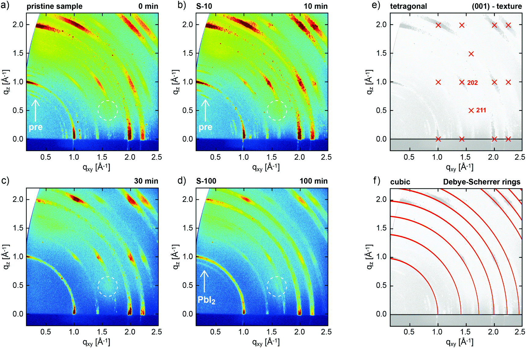 | ||
| Fig. 1 2D GIXRD patterns of CH3NH3PbI3−xClx perovskite films, as obtained from a precursor solution of CH3NH3I and PbCl2 (3:1) in DMF, (a) without annealing, and annealed at 100 °C for (b) 10 min, (c) 30 min, and (d) 100 min. (e) Simulated GIXRD pattern of tetragonal perovskite in (001) texture, and (f) calculated Debye–Scherrer rings (non-textured case) for (pseudo-)cubic perovskite.28 Arrows in (a and b) exemplarily mark additional diffraction features assigned to perovskite precursors, dotted circles highlight the expected position of the tetragonal (211) reflection, and the arrow in (d) marks a ring assigned to PbI2 related to the degraded perovskite. | ||
We investigated pristine (not-annealed) (Fig. 1a) films and those annealed at 100 °C for 10 min (S-10, Fig. 1b), 30 min (Fig. 1c), and 100 min (S-100, Fig. 1d). In all cases, GIXRD shows the growth of the perovskite in pronounced fiber texture, i.e., a common plane of its crystal structure is preferentially oriented parallel to the substrate (with random azimuthal orientation of the crystallites). This growth mode is deduced from the presence of regions of strongly enhanced intensity on the diffraction rings (Debye–Scherrer rings) in Fig. 1a–d, which, within the error margin of the present experiment, can be well indexed both with a (pseudo-)cubic and a tetragonal polymorph, as repeatedly observed for perovskite films.30Fig. 1e shows the expected peak positions calculated for the tetragonal polymorph in (001) texture as used to indexing our data. The observation of the (211) reflection at the indicated position acts as fingerprint for tetragonal instead of cubic perovskite. For the latter, this reflection would occur at a far different position.31 The structure factors calculated for the (211) and (202) reflections (cf.Fig. 1e), and, therefore, the expected diffraction intensities, are essentially identical in the tetragonal crystal structure. In the present GIXRD data, however, the diffraction intensity at the expected (211) position (dotted circles in Fig. 1a–d) is negligible compared to that of (202), which demonstrates that in our samples perovskite predominantly grows in a (pseudo-)cubic polymorph in (001)-texture; the corresponding calculated Debye Scherrer rings depicted in Fig. 1f match the experimental data reasonably well. Due to the high surface sensitivity of the technique, no contributions from the underlying ITO substrate are observed; GIXRD reference data for the bare PEDOT:PSS/ITO substrate are shown in the ESI,† Fig. S1.
Apart from the perovskite-derived diffraction pattern, for both the pristine sample and S-10 we observe additional features (cf.Fig. 1a and b), which, however, cannot be unambiguously assigned. Both the crystal structures of pristine CH3NH3I and PbCl2 cannot be held to index these additional reflections.32,33 In literature,24,34 the additional features were assigned to a “crystalline precursor structure” that readily transforms into perovskite upon thermal annealing but could not further be crystallographically specified. Interestingly, one of these diffraction features at q = 1.1 Å−1 does agree with the calculated position of MAPbCl3,25 which is an intermediate phase assumed to be crucial for the completion of film formation in solution-processed mixed-halide perovskite.24 Importantly, for annealing times over 30 min all precursor features vanish (Fig. 1c and d) and the film appears to be fully converted into MAPbI3 perovskite. For S-100 (100 min annealing), a faint ring at q = 0.9 Å−1 indicates the emergence of PbI2,35 a known degradation product of MAPbI3 upon annealing.24
Since the mixed-halide perovskite film structure at 10 min annealing time, i.e. before complete film formation, is significantly different from the film structure after 100 min, when the crystallization is completed and no further structure evolution is observed (except for growing PbI2 content), we applied spatially resolved chemical composition analysis to samples S-10 and S-100 in lateral and vertical direction.
3.2. Morphology, interface and composition analysis
ToF-SIMS analysis was conducted to characterize the perovskite sample composition in 3D before (S-10) and after complete crystallization (S-100). In ToF-SIMS profiles in the surface normal direction, for each sputter step (corresponding to a sputter time), the intensity of selected secondary ions over the analyzed area is represented as a data point in the profile. The sputter time can be directly translated into the probed sample depth if the sputtering rate is constant, i.e., within a given homogeneous material. A low-energy Cs+ beam has been demonstrated to allow for convenient sputtering rates both on organic and inorganic materials while preserving a high yield for characteristic high-mass molecular fragments.36,37Fig. 2 shows the ToF-SIMS profiles obtained for selected masses on S-10 and S-100. Fragments were carefully selected to identify the dominating MAPbI3 perovskite phase (PbI3−), the PEDOT:PSS layer (C4H4S−), and the ITO substrate (In2O2−) while avoiding mass overlaps. In the not-fully-crystallized perovskite (S-10), fragment ions from the inorganic compound (PbCl2 or its derivative) are still present. The distribution of PbCl2 and other related compounds was assessed by selecting and reconstructing the PbCl3− signal distribution. CN− was chosen to identify the organic MA; this low-mass fragment, however, is not specific to a structure as it could either come from the perovskite, or from other compounds such as MACl, MAI, MAPbCl3, etc.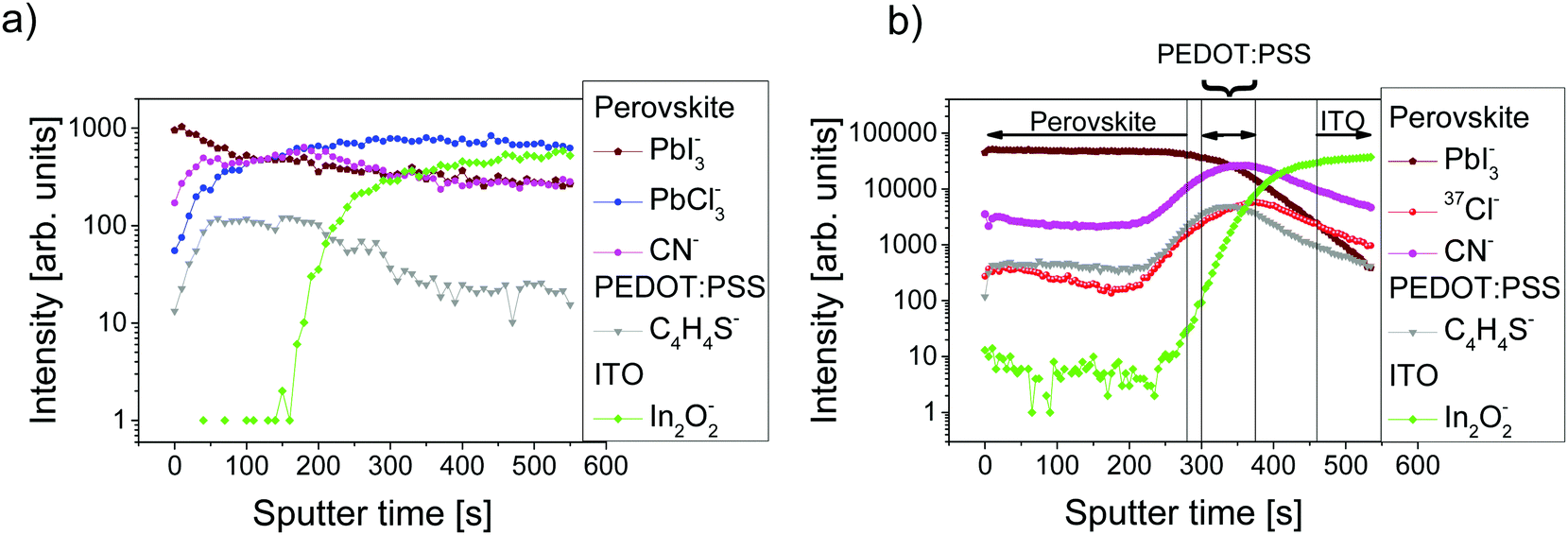 | ||
| Fig. 2 ToF-SIMS depth profiles of sample (a) S-10 and (b) S-100: interfaces between the different layers are identified by looking at the intensities of characteristic ion (PbI3−, C4H4S−, and In2O2− for the perovskite, PEDOT:PSS, and ITO layers, respectively), as shown by the vertical lines (intensity ≥80% of its respective maximum value). | ||
In the ToF-SIMS profile of S-10 (Fig. 2a), PbI3−, PbCl3−, and CN− are detected with relatively constant intensities during the whole sputtering process, in contrast to C4H4S− (indicative of PEDOT:PSS), which shows a drop of intensity after 250 s sputter time. Thus, the precursor/perovskite layer in S-10 consists of PbCl3-based compounds, MA, and already formed MAPbI3 perovskite (as inferred from GIXRD). The detection of C4H4S− already from the beginning of the experiment for both samples S-10 and S-100 (Fig. 2a and b) demonstrates the high sensitivity (up to 1 ppm) of ToF-SIMS, as no signal related to PEDOT:PSS was detected by XPS measurements (cf. S 2p core level spectra in Fig. S2, ESI†). While the intensities of the secondary ions of both samples are not quantitatively comparable, the trends of the depth profiles allow drawing qualitative conclusions. In the ToF-SIMS profile of S-10 (Fig. 2a), the signal from the PEDOT:PSS raises after few seconds of sputtering, while it increases only after 250 s for S-100 (Fig. 2b). This observation implies that the precursor/perovskite layer does not cover the PEDOT:PSS completely after 10 min annealing. AFM investigations confirm this hypothesis (Fig. 3). The AFM micrograph from S-10 evidences the presence of pinholes and cavities (circles and squares in Fig. 3b). The high surface corrugation of the precursor/perovskite film (root mean square roughness RS = 46 nm) explains the nearly simultaneous detection of both perovskite- and the PEDOT:PSS-related ions in ToF-SIMS (Fig. 2a). The sputtering process tends to carry on the high roughness of the initial surface. In contrast, the AFM micrograph of a not-annealed sample (Fig. 3a) shows needle structures with large voids in between; this translates into a substantially higher roughness (RS = 90 nm). With increasing annealing time the roughness of the films is significantly reduced (S-10: 46 nm, S-100: 23 nm), as shown in Fig. 3b and c. Annealing the sample leads to a more homogeneous surface coverage, thus explaining the initially much lower signal from the PEDOT:PSS layer in the ToF-SIMS profile of S-100, as mentioned above.
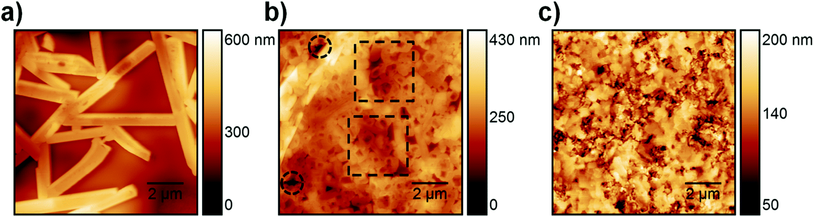 | ||
| Fig. 3 AFM micrographs of samples annealed during (a) 0 min, (b) 10 min (circles and squares indicate pinholes and cavities, respectively) and (c) 100 min with an overall root mean square roughness RS of 90 nm (0 min), 46 nm (10 min) and 23 nm (100 min), respectively. | ||
In contrast to S-10, we see from the ToF-SIMS profiles in Fig. 2b that the interfaces between the individual layers of S-100 can be better discriminated (see vertical lines in Fig. 2b), where each layer is identified by the region where the corresponding ion (perovskite: PbI3−, PEDOT:PSS: C4H4S−, ITO: In2O2−) has intensities higher than 80% of its maximum value. The interface with PEDOT:PSS marked by the C4H4S− intensity plateau is reached in S-100 after about 300 s sputtering (Fig. 2b) while it appears almost from the beginning of the depth profile in S-10.
Importantly, while the chlorine concentration in the perovskite layer deduced from the ToF-SIMS depth profiles for S-100 (Fig. 2b) is only slightly above the detection limit and can be well ascribed to contamination, we find a significant accumulation of chlorine (37Cl− signal) from the precursor/perovskite within the PEDOT:PSS layer (C4H4S− signal) and at the interface, as both signals have comparable trends. As an aside we note that it was argued before whether the term “mixed halide perovskite” is still tenable for perovskite obtained from chlorine-based precursors.12,38 Despite our results for the S-100 film, where chlorine is found to be only present at the substrate interface, we retain this wording here, in order to highlight the relevance of chlorine in the formation process of perovskite. Since the Cl− ionization yield is very high and the ToF-SIMS technique is semi-quantitative (as applied here), it is worthy to stress that in a reference film of pristine PEDOT:PSS (i.e., without a precursor/perovskite overlayer) on ITO, an 18 times lower relative chlorine content is found (ESI,† Fig. S3). This excludes that the chlorine signal measured in the PEDOT:PSS layer of S-100 is due to contamination. For S-10, the ToF-SIMS profile of 37Cl− follows that of PbCl3− suggesting that both ions represent the same species (ESI,† Fig. S4). For S-100, the profile of CN− has the same trend as that of 37Cl− (Fig. 2b), thus indicating that chlorine is present most likely in the form of MACl both at the precursor/perovskite-PEDOT:PSS interface and within the PEDOT:PSS layer.
It has been reported that even a low chlorine concentration allegedly can significantly improve the charge-transport properties of perovskite films.12 Particularly, the presence of chlorine at the perovskite interface to the substrate has been suggested to promote the charge collection at the interface.21 The “chlorine loss” in the final mixed-halide MAPbI3−xClx perovskite film has already been discussed in several studies,13,17,39 where a sublimation of, e.g., MACl, during the annealing step has been proposed to explain this loss.13,20,39 Fully in line with literature,13,20 our XPS measurements on S-100 did not reveal any presence of chlorine above the detection limit (see below). Nevertheless, the presence of residual chlorine within the final MAPbI3−xClx perovskite has been experimentally assessed by X-ray absorption near-edge structure (XANES).40 The chlorine location, however, could not be determined with precision yet. A strong spatial inhomogeneity in the chlorine concentration throughout a 60 nm thin perovskite film was deduced from hard X-ray photoelectron spectroscopy combined with fluorescence yield X-ray absorption spectroscopy.22 To test the theoretical assumption assessing the interfacial role of chloride, Colella et al. conducted angle-resolved XPS measurement on a 5 nm thin perovskite film and detected chloride at the perovskite TiO2 interface.21 However, such a film thickness does not reflect real device applications. As reported here, the ToF-SIMS analysis, in contrast to surface sensitive XPS techniques, allows to track the chlorine content throughout the entire perovskite layer depth and into the underlying hole transport layer in a sample with a perovskite film of device-relevant thickness (∼250 nm).8,14 This could support the notion of improved charge transport due to chlorine presence in devices based on MAPbI3−xClx perovskite films. The increase in 37Cl− signal intensity down towards and within the PEDOT:PSS layer itself, as observed here, resembles the chlorine diffusion observed in mesoporous TiO2 of a perovskite-based solar cell with the structure (Au/hole-transport-material/perovskite/TiO2).28 This congruence points towards similar chlorine diffusion dynamics, independent of substrate and device configuration, and thus also corroborates the idea that chlorine affects the interfacial electronic structure by modifying the perovskite/substrate interface.21 This provides support for the prominence of mixed-halide MAPbI3−xClx perovskite-based solar cells in comparison to their single halide MAPbI3 perovskite counterpart.
Further spatial analysis of the sample composition was performed by depth-integrating the intensity of the selected ion for a given area. These 2D ToF-SIMS maps for PbI3−, PbCl3− and CN− of S-10 (Fig. 4) disclose a lateral phase separation occurring in the precursor/perovskite layer after 10 min annealing. Two regions, A and B, can be distinguished: region A (red squares) is characterized by high PbI3− and low PbCl3− intensities while the opposite applies in region B (blue circles). Hence, we assign region A to the already formed perovskite MAPbI3, the presence of which was already established by GIXRD analysis (vide supra).
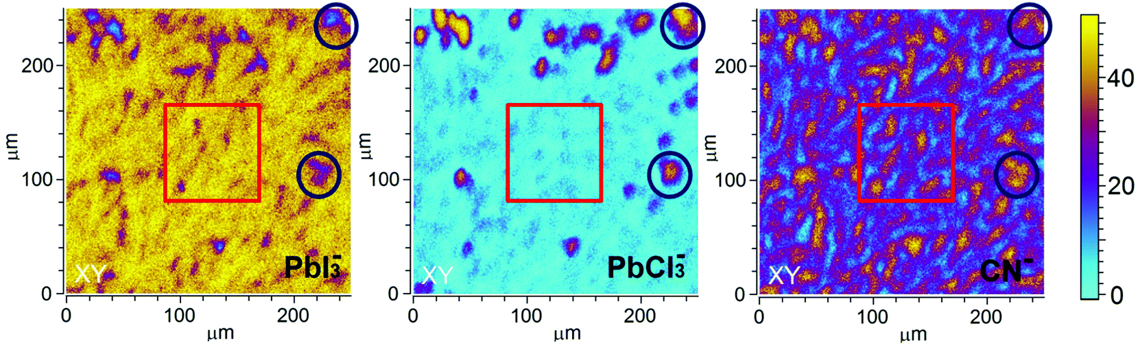 | ||
| Fig. 4 ToF-SIMS 2D (XY) maps taken on S-10 displaying the depth-integrated intensity of the selected ions. The lateral resolution is about 1 μm. Red squares indicate a region (A in the text) characterized by high PbI3− and CN− intensities and a low PbCl3− intensity; blue circles indicate regions (B in the text) where PbCl3− and CN− intensities are high and that of PbI3− low. | ||
We assume that the high PbCl3− ion intensity in region B could either be due to the fragmentation of MAPbCl3 or to the presence of the original inorganic compound PbCl2. Note that the latter rationale agrees well with the presence of PbCl2 nanoparticles in PbCl2-based perovskite precursor solution, as reported by Tidhar et al.27 It has been suggested that due to the lower solubility of PbCl2, such nanoparticles are still present in the precursor solution and serve as nucleation centers, promoting the formation of crystalline perovskite.
At this point, results do not allow ruling out the hypothesis that the measured PbCl3− signal comes from the fragmentation of MAPbCl3; the presence of MAPbCl3 acting as an intermediate phase has been indeed confirmed by the GIXRD analysis. To address this question, the distribution of organic MA halide species (MAX) in S-10 was monitored by following the high-yield CN− ion XY-distribution (see right panel in Fig. 4). Fig. 4 shows that regions exist (circles), where PbCl3− and CN− signals are simultaneously high, and, likewise, regions (squares) where this is true for the PbI2− and CN− signals. Therefore, CN− is present in both regions (A, B). In region A, CN− may originate from the fragmentation of MAPbI3 perovskite or MAI (compound in excess). This latter assumption is further supported by the XY-reconstruction of CH3NH2− (de-protonated MAI) in Fig. S5 (ESI†) that indicates a spatial distribution very similar to the one of PbI3−. In region B, CN− stems from the fragmentation of methyl ammonium from intermediate compounds such as MACl or MAPbCl3 related to the crystalline precursor structure,12,17,24 as observed by GIXRD analysis. Since such an XY-reconstruction of CH3NH2Cl− (MACl compound) could not be performed due to its extremely low intensity, we assume that region B is dominated by MAPbCl3 and possibly PbCl2. Our results are in line with the topotactic transformation proposed by Moore et al.19 and Williams et al.17 In their model, the authors suggest the co-presence of a chloride-rich phase with a peripheral iodide-rich phase during annealing. By diffusion of MA+ and I− from the latter to the former (with the chloride being volatile), a more stabilized iodide-rich phase evolves with an enhanced film crystallization, in contrast to chlorine-free single MAPbI3 perovskite. The intermediate chloride-rich phase therefore acts as a preceding structural template for the final MAPbI3 perovskite. In contrast to the study of Williams et al.17 describing a variation in the vertical composition of mixed-halide perovskite films during annealing, our results point towards the coexistence of lead chloride-rich and lead iodide-rich phases right throughout the film depth (see also the YZ cross-section map in Fig. S6 in the ESI†), as we schematically illustrate in Fig. 5a.
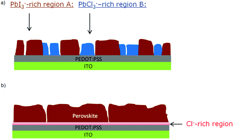 | ||
| Fig. 5 Simplified schematic cross-sections as resulted from ToF-SIMS 2D imaging: (a) illustrates the lateral phase separation between region A, corresponding to already formed MAPbI3 perovskite and region B, where perovskite has not formed yet for S-10; and (b) shows a homogeneous composition and a lower surface roughness for S-100. | ||
These findings underline the importance of chloride for the formation of highly textured films, which are crucial for enhancing the photovoltaic performance of perovskite-based solar cells.41 The annealing is associated with the chlorine migration towards the interface of perovskite and the PEDOT:PSS layer (which acts as hole transport layer here), while the remaining Pb recombines with MA+ and I− to form the MAPbI3 perovskite. As shown by the XY maps of S-100 (Fig. S7, ESI†), when the crystallization is completed, the perovskite film does no longer show any phase separation (see Fig. 5b).
3.3. Electronic structure and composition analysis by photoemission
By combining XPS and UPS, we independently explored the influence of the annealing time not only on the chemical composition but also on the electronic structure of the resulting films.For both S-10 and S-100 samples, no chlorine was detected from the Cl 2p core level spectra in Fig. 6a, evidencing the inadequacy of XPS in detecting minute amounts of an element as opposed to ToF-SIMS (vide supra); further core levels (I 3d, Pb 4f and N 1s) are shown in Fig. 6b–d. Notably, for S-10 the binding energy (BE) of the I 3d7/2 (at 619.1 eV) and the N 1s (at 401.9 eV) core levels increased by 0.7 eV, and that of Pb 4f (at 138.1 eV) by 0.6 eV with prolonged annealing time (S-100). Very much alike, the valence band onset (VBonset) shifted to the same direction relative to the Fermi level (EF) by 0.5 eV when going from S-10 to S-100, and the work function Φ decreased by ca. 0.4 eV (Fig. 6e and f). Since all electronic levels (core and valence) shift towards higher BE from S-10 to S-100 by approximately the same amount, the cause for the shift is most likely of electrostatic nature. Given the direction of the shift, the material becomes more n-type upon full conversion to the perovskite. The small difference in shift between core and valence levels is accounted for by the concomitant overall change of the valence electronic structure. The fact that the work function change is lower than the shift of all electronic levels points towards a change in the surface electrostatic potential due to structural/compositional changes in addition to the modified doping level.
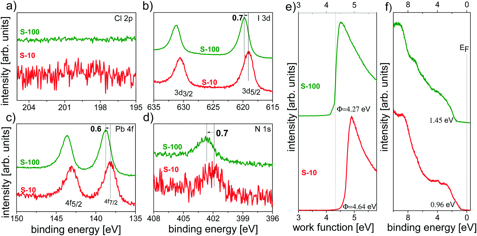 | ||
| Fig. 6 Photoemission spectra of perovskite samples annealed at 100 °C for 10 min (S-10) and 100 min (S-100). XPS core level spectra of (a) Cl 2p, (b) I 3d, (c) Pb 4f, and (d) N 1s. UPS (e) SECO spectra and (f) valence spectra. | ||
Note that such an electronic-structure modification with annealing time has been suggested before,25 based on the argument that an MAI deficit n-dopes perovskite films,42i.e., MA sublimation upon annealing renders the film more n-type. We further observe a concomitant (small) increase (+0.12 eV) in the ionization energy (IE = Φ + VBonset) with annealing time, which can be related to the variation of the perovskite-film stoichiometry (in particular, MA+ deficiency) as was recently suggested.43 This assumption is corroborated by ToF-SIMS analysis by displaying the CN− to PbI3−-ratio (CN−/PbI3−) XY image for S-10 and S-100 (Fig. S8, ESI†). In comparison to S-100, regions exist in S-10 where the relative CN− content is higher, indicating that an overall lower MA content is found after longer annealing time.
4. Conclusion
The present study provides insights into the nucleation of the MAPbI3−xClx mixed-halide perovskite. The evolution of structure, morphology, chemical composition, and electronic structure of precursor and perovskite films was investigated before, during, and after complete conversion. With annealing time, solution-processed perovskite films were found to evolve from an inhomogeneous composition characterized by laterally separated MAPbI3 perovskite and lead chloride-rich domains, to a single phase corresponding to a fully crystallized perovskite after 100 min of annealing at 100 °C. In particular, this very evolution of the film composition was associated with evident changes of its crystal structure, which corroborates the crucial role of PbCl2 for initiating perovskite nucleation and the importance of intermediate phases, particularly MAPbCl3, for the formation of highly uniform and textured perovskite film, which is essential for attaining high-performance perovskite solar cells.Relative deficiencies in MA content were found to modify the electronic structure and promote the formation of more n-type films with increasing annealing time. Noteworthy, some chlorine always stays in the annealed films even after the full crystallization process; this was enabled by the use of ToF-SIMS with much higher sensitivity than XPS. Before the complete perovskite conversion, chlorine from the inorganic lead chloride compound and intermediate phases was detected in isolated regions as evidenced by ToF-SIMS 2D maps, whereas after completion of the perovskite film formation, chlorine was mostly located at the interface to and within the underlying PEDOT:PSS layer. These results corroborate not only the key role of chlorine in the formation of solution-processed mixed-halide MAPbI3−xClx perovskite films but also its suggested implication in the optoelectronic properties of perovskite-based solar cells, thus highlighting the importance of controlling the annealing conditions and duration for optimizing perovskite film preparation.
Acknowledgements
This work was supported by the Helmholtz Energy Alliance “Hybrid Photovoltaics”, the SFB951 (DFG), and the HZB-HU Graduate School “hybrid4energy”.References
- M. A. Green, K. Emery, Y. Hishikawa, W. Warta and E. D. Dunlop, Prog. Photovolt. Res. Appl., 2016, 24, 905–913 CrossRef.
- J. Burschka, N. Pellet, S.-J. Moon, R. Humphry-Baker, P. Gao, M. K. Nazeeruddin and M. Grätzel, Nature, 2013, 499, 316–319 CrossRef CAS PubMed.
- M. Liu, M. B. Johnston and H. J. Snaith, Nature, 2013, 501, 395–398 CrossRef CAS PubMed.
- Q. Chen, H. Zhou, Z. Hong, S. Luo, H.-S. Duan, H.-H. Wang, Y. Liu, G. Li and Y. Yang, J. Am. Chem. Soc., 2014, 136, 622–625 CrossRef CAS PubMed.
- L. Liu, J. A. McLeod, R. Wang, P. Shen and S. Duhm, Appl. Phys. Lett., 2015, 107, 61904 CrossRef.
- A. Kojima, K. Teshima, Y. Shirai and T. Miyasaka, J. Am. Chem. Soc., 2009, 131, 6050–6051 CrossRef CAS PubMed.
- H. J. Snaith, J. Phys. Chem. Lett., 2013, 4, 3623–3630 CrossRef CAS.
- J. You, Z. Hong, Y. M. Yang, Q. Chen, M. Cai, T.-B. Song, C.-C. Chen, S. Lu, Y. Liu, H. Zhou and Y. Yang, ACS Nano, 2014, 8, 1674–1680 CrossRef CAS PubMed.
- H. Zhou, Q. Chen, G. Li, S. Luo, T. Song, H.-S. Duan, Z. Hong, J. You, Y. Liu and Y. Yang, Science, 2014, 345, 542–546 CrossRef CAS PubMed.
- D. P. McMeekin, G. Sadoughi, W. Rehman, G. E. Eperon, M. Saliba, M. T. Hörantner, A. Haghighirad, N. Sakai, L. Korte, B. Rech, M. B. Johnston, L. M. Herz and H. J. Snaith, Science, 2016, 351, 151–155 CrossRef CAS PubMed.
- M. M. Lee, J. Teuscher, T. Miyasaka, T. N. Murakami and H. J. Snaith, Science, 2012, 338, 643–647 CrossRef CAS PubMed.
- S. Colella, E. Mosconi, P. Fedeli, A. Listorti, F. Gazza, F. Orlandi, P. Ferro, T. Besagni, A. Rizzo, G. Calestani, G. Gigli, F. De Angelis and R. Mosca, Chem. Mater., 2013, 25, 4613–4618 CrossRef CAS.
- H. Yu, F. Wang, F. Xie, W. Li, J. Chen and N. Zhao, Adv. Funct. Mater., 2014, 24, 7102–7108 CAS.
- S. D. Stranks, G. E. Eperon, G. Grancini, C. Menelaou, M. J. P. Alcocer, T. Leijtens, L. M. Herz, A. Petrozza and H. J. Snaith, Science, 2013, 342, 341–344 CrossRef CAS PubMed.
- D. Song, J. H. Heo, H. J. Han, M. S. You and S. H. Im, J. Power Sources, 2016, 310, 130–136 CrossRef CAS.
- B. Park, B. Philippe, T. Gustafsson, K. Sveinbjörnsson, A. Hagfeldt, E. M. J. Johansson and G. Boschloo, Chem. Mater., 2014, 26, 4466–4471 CrossRef CAS.
- S. T. Williams, F. Zuo, C.-C. Chueh, C.-Y. Liao, P.-W. Liang and A. K.-Y. Jen, ACS Nano, 2014, 8, 10640–10654 CrossRef CAS PubMed.
- B. Philippe, B.-W. Park, R. Lindblad, J. Oscarsson, S. Ahmadi, E. M. J. Johansson and H. Rensmo, Chem. Mater., 2015, 27, 1720–1731 CrossRef CAS.
- D. T. Moore, H. Sai, K. W. Tan, L. A. Estroff and U. Wiesner, APL Mater., 2014, 2, 81802 CrossRef.
- E. L. Unger, A. R. Bowring, C. J. Tassone, V. L. Pool, A. Gold-Parker, R. Cheacharoen, K. H. Stone, E. T. Hoke, M. F. Toney and M. D. McGehee, Chem. Mater., 2014, 26, 7158–7165 CrossRef CAS.
- S. Colella, E. Mosconi, G. Pellegrino, A. Alberti, V. L. P. Guerra, S. Masi, A. Listorti, A. Rizzo, G. G. Condorelli, F. De Angelis and G. Gigli, J. Phys. Chem. Lett., 2014, 5, 3532–3538 CrossRef CAS PubMed.
- D. E. Starr, G. Sadoughi, E. Handick, R. G. Wilks, J. H. Alsmeier, L. Köhler, M. Gorgoi, H. J. Snaith and M. Bär, Energy Environ. Sci., 2015, 8, 1609–1615 CAS.
- M. Saliba, K. W. Tan, H. Sai, D. T. Moore, T. Scott, W. Zhang, L. A. Estroff, U. Wiesner and H. J. Snaith, J. Phys. Chem. C, 2014, 118, 17171–17177 CAS.
- K. W. Tan, D. T. Moore, M. Saliba, H. Sai, L. A. Estroff, T. Hanrath, H. J. Snaith and U. Wiesner, ACS Nano, 2014, 8, 4730–4739 CrossRef CAS PubMed.
- P. P. Atittaya Naikaew, Appl. Phys. Lett., 2015, 106, 232104 CrossRef.
- D. Khatiwada, S. Venkatesan, N. Adhikari, A. Dubey, A. F. Mitul, L. Mohammad, A. Iefanova, S. B. Darling and Q. Qiao, J. Phys. Chem. C, 2015, 119, 25747–25753 CAS.
- Y. Tidhar, E. Edri, H. Weissman, D. Zohar, G. Hodes, D. Cahen, B. Rybtchinski and S. Kirmayer, J. Am. Chem. Soc., 2014, 136, 13249–13256 CrossRef CAS PubMed.
- F. Matteocci, Y. Busby, J.-J. Pireaux, G. Divitini, S. Cacovich, C. Ducati and A. Di Carlo, ACS Appl. Mater. Interfaces, 2015, 7, 26176–26183 CAS.
- B. Yang, J. Keum, O. S. Ovchinnikova, A. Belianinov, S. Chen, M.-H. Du, I. N. Ivanov, C. M. Rouleau, D. B. Geohegan and K. Xiao, J. Am. Chem. Soc., 2016, 138, 5028–5035 CrossRef CAS PubMed.
- C. C. Stoumpos, C. D. Malliakas and M. G. Kanatzidis, Inorg. Chem., 2013, 52, 9019–9038 CrossRef CAS PubMed.
- T. Baikie, Y. Fang, J. M. Kadro, M. Schreyer, F. Wei, S. G. Mhaisalkar, M. Graetzel and T. J. White, J. Mater. Chem. A, 2013, 1, 5628–5641 CAS.
- O. Yamamuro, T. Matsuo, H. Suga, W. I. F. David, R. M. Ibberson and A. J. Leadbetter, Acta Crystallogr., Sect. B: Struct. Sci., 1992, 48, 329–336 CrossRef.
- R. L. Sass, E. B. Brackett and T. E. Brackett, J. Phys. Chem., 1963, 67, 2863–2864 CrossRef CAS.
- Y.-C. Huang, C.-S. Tsao, Y.-J. Cho, K.-C. Chen, K.-M. Chiang, S.-Y. Hsiao, C.-W. Chen, C.-J. Su, U.-S. Jeng and H.-W. Lin, Sci. Rep., 2015, 5, 13657 CrossRef PubMed.
- Z. Zheng, A. Liu, S. Wang, Y. Wang, Z. Li, W. M. Lau and L. Zhang, J. Mater. Chem., 2005, 15, 4555–4559 RSC.
- Y. Busby, S. Nau, S. Sax, E. J. W. List-Kratochvil, J. Novak, R. Banerjee, F. Schreiber and J.-J. Pireaux, J. Appl. Phys., 2015, 118, 75501 CrossRef.
- C. Noël and L. Houssiau, J. Am. Soc. Mass Spectrom., 2016, 27, 908–916 CrossRef PubMed.
- M. Grätzel, Nat. Mater., 2014, 13, 838–842 CrossRef.
- A. Dualeh, N. Tétreault, T. Moehl, P. Gao, M. K. Nazeeruddin and M. Grätzel, Adv. Funct. Mater., 2014, 24, 3250–3258 CrossRef CAS.
- V. L. Pool, A. Gold-Parker, M. D. McGehee and M. F. Toney, Chem. Mater., 2015, 27, 7240–7243 CrossRef CAS.
- P. Docampo, F. C. Hanusch, N. Giesbrecht, P. Angloher, A. Ivanova and T. Bein, APL Mater., 2014, 2, 81508 CrossRef.
- Q. Wang, Y. Shao, H. Xie, L. Lyu, X. Liu, Y. Gao and J. Huang, Appl. Phys. Lett., 2014, 105, 163508 CrossRef.
- J. Emara, T. Schnier, N. Pourdavoud, T. Riedl, K. Meerholz and S. Olthof, Adv. Mater., 2016, 28, 553–559 CrossRef CAS PubMed.
Footnote |
| † Electronic supplementary information (ESI) available. See DOI: 10.1039/c6cp06347k |
| This journal is © the Owner Societies 2017 |