
 Open Access Article
 This Open Access Article is licensed under a Creative Commons Attribution-Non Commercial 3.0 Unported Licence
Energy harvesting and conversion mechanisms for intrinsic upconverted mechano-persistent luminescence in CaZnOS
Bolong
Huang
Department of Applied Biology and Chemical Technology, The Hong Kong Polytechnic University, Hung Hom, Kowloon, Hong Kong SAR, China. E-mail: bhuang@polyu.edu.hk
First published on 25th August 2016
Abstract
We interpreted the mechanisms of energy harvesting and conversion for intrinsic upconverted mechano-persistent luminescence in CaZnOS through a native point defects study. We found that vacancy defects such as Zn and O vacancies, as well as Schottky pair defects, act as energy harvesting centers; they are very readily formed and very active. They are found to be extra deep electron or hole trap levels near the valence or conduction band edges, respectively. This leads to a coupling and exchange effect to continuously collect and transport host charges along a path via localized states to deep recombination levels. The initiating energy barrier is small and can be overcome by ambient thermal stimulation or quantum tunneling. Native activators such as V2+O, V2+ZnO, and V2+CaZnOS function as energy conversion centers to transfer energy into photon emissions. This gives a solid theoretical reference for developing upconverted mechano-persistent luminescence.
Introduction
Mechanoluminescence (ML) is related to an optical phenomenon where the charge carriers from the host lattice in a material are usually excited with higher energy piezoelectricity in the form of friction-related tribo-stimulation or external man-made stress/pressure.1–6 Such materials can accommodate external UV light (ultraviolet) photo-irradiation or near-infra-red (NIR) photo-stimulation with a wavelength of 980 nm. The resulting visible luminescence occurs by photon emission. The excited charge carriers will be released for further recombination through the delocalized conduction states of the host lattice by a small amount of thermal stimulation or quantum tunneling effects. With accurate modulation of external mechanical stimulation in terms of physical parameters, ML will provide a wide platform of applications in the fields of earthquake prediction, stability tests of large buildings or bridges, and hand-input oriented multi-touch technology in smartphones or other mobile devices, combined with electronics and magneto-opt-electronics.7–9Recent studies performed by Xu et al.5,10 demonstrated a substantial leap in this field, showing that some ML materials, such as oxy-sulfides, can also be applied as persistent luminescence materials through transition metal doping and have flexible color manipulations.11 This requires us not only to understand the electronic structures that originate from extrinsic doping, but also makes it highly necessary to plot the photon-electron dynamic transitions based on the subtle energy conversion mechanisms during the process of persistent luminescence.
Currently, stronger intensity, longer time and lower cost with flexible wavelength in persistent luminescence are increasingly needed as the demands of electronic device integration, biochemistry and materials engineering rapidly expand.12–22 Upconverted mechano-persistent luminescence (UMPL), which is based on the long-decay-time phosphorescence concept,14,15,23,24 is challenging to downscale to smaller nanosized particle synthesis with faster charge response, lower cost and longer time for luminescence or mechanical signal imaging. For a long time, the luminescence of lanthanide oxide materials has actually been an important subject in optical applications and spectroscopy studies.25–29 The lanthanide rare-earth (RE) ions-assisted phosphor luminescence technique has aroused tremendous interest in biological, chemical and physical applications; this technique plays a leading role in modulating luminescence properties.30 Therefore, it is a feasible technology to achieve by smart combinations, as explored by Pan et al.,3,6 based on rare-earth ion doping. The similar host materials they used (CaZnOS) with activated Eu2+ can give high color rendering when excited by blue LED.31
However, this technique remains the pattern of experimental attempts, with combinations of host materials and RE-based activating dopant ions.32 Although over 200 combinations have been achieved, with a steady increase in production, the performance modulations still lack solid theoretical support and guidance regarding chemical trends during synthesis.15 Moreover, the relationship between their native defect level-assisted electron transport and their upconverted persistent luminescence properties is also still far from being well understood, especially at the electronic level. This knowledge gap not only impedes the process of designing new generations of persistent luminescence based on UMPL, but also prevents the further development of existing technology. Further investigations to fill this gap are of great significance to the relevant science and technological applications.
The interplay effect of different point defect levels is a significant issue. In a previous study,33 we found that native point defects in the host materials not only produce a local lattice distortion or charge density anomalies, but also induce unique localized electronic levels in the optical fundamental band gaps, which are either occupied or empty. Therefore, the stabilities and concentrations of native point defects of the host materials in persistent phosphor studies are quite important. Our previous study shows that some lathandide oxides themselves present persistent luminescence, especially based on the unusual up-conversion character of their electron transport.34 Accordingly, this persistent luminescence is attributed to the subtle interplay of different native point defect states, based on the findings of our previous investigations.33,35,36
A driving force for extensive theoretical investigation relates to the current consensus summarized by experiments, which is that two dominant factors determine the performance of UMPL materials: activators and traps. The emission is controlled by the activator, and the width of the inter-levels determines the wavelength (photon energy). The trap center given by either native point defects or dopants is the factor that modulates the duration time and intensity of the persistent luminescence. Significantly, Maldiney et al. accomplished the modulation of the time-decay parameter of persistent luminescence37 in their recent work, which indicated to us that it is possible to modify the performance of these materials through systematic modification of the depths of charge trap levels relative to the conduction band (CB) edge. Our new interest in the native point defects of luminescent solids is firmly supported by progress.
The exact inter-levels of activators and traps within the electronic structures suggested by theoretical study will provide a reference for the selection of such structures with optimal performance.33,34,38,39 Therefore, it is necessary to open a preliminary discussion on the different native point defects in a potential UMPL to examine its energy conversion mechanism and to provide a useful reference for further experiments and various applications.33,34,38,39
In this work, we discuss luminescence models covering the range from the typical oxygen vacancy (VO) related F-center to other potential energy conversions through different optical transitions. Due to strong electron-phonon coupling, widened optical transitions result from the Stokes shift between the absorption and emission spectra,40 and the analytical mechanism is still not clear by current theoretical methods. Accordingly, another important issue to be addressed is the energy conversion-related defect reaction model for persistent luminescence, to find the nearly continuous energy source supporting long-time optical transition and lengthened electronic transport.
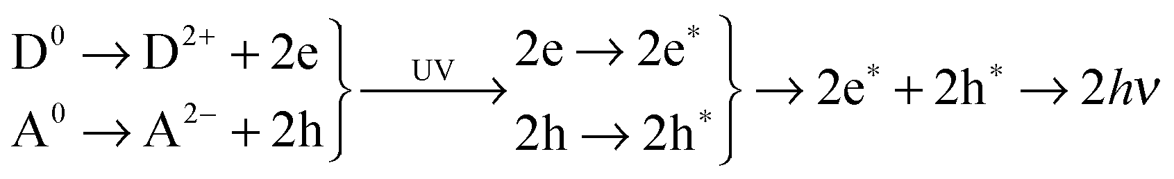
Our previous study shows if defect-related transitions follow the closed cycle of the zero-phonon line (ZPL) between different optical transition states, the optical absorption and emission will be accomplished with a large efficiency in both optical quantum yield and energy conversion.34 The lattice distortions between these reactions will support electron transfer between different optical transition levels with exact amounts of negative effective correlation energy (−Ueff), ideally, as shown in Fig. 1. The native complementary charged point defects form a time-accumulated donor–acceptor pair (DAP) and produce band-like levels within the optical band gaps of the host materials. They pin the activator inter-levels at specific positions of the band gap in the form of a −Ueff optical transition along this closed-ZPL-cycle. A similar concept has been successfully utilized in other solid functional materials in our theoretical modeling.34,41–43
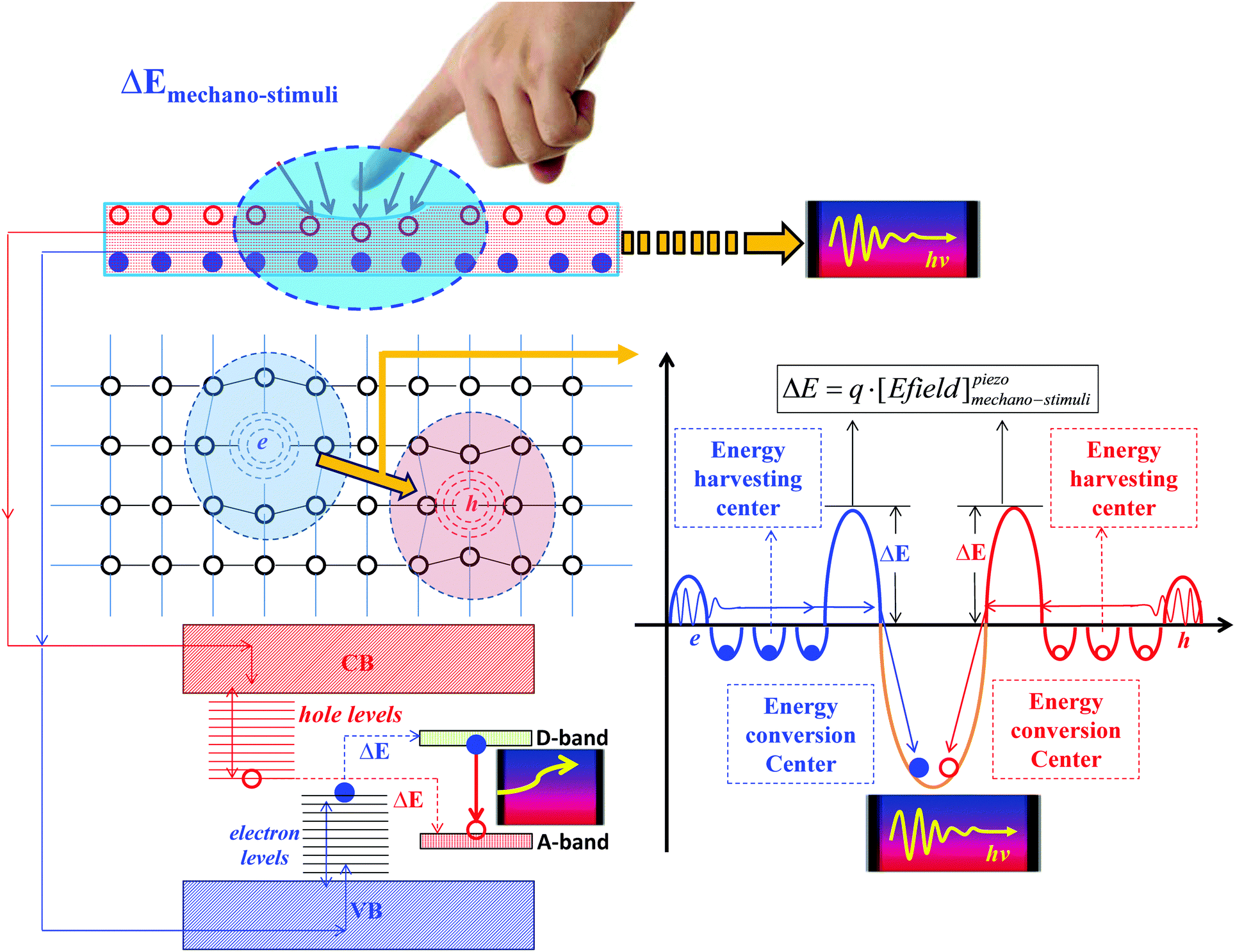 | ||
| Fig. 1 Schematic of the native point defect-induced energy harvesting and conversion model for upconverted mechano-persistent luminescence. | ||
The key difference between UMPL materials and conventional PL materials is that the electrons and holes can be separated and allocated at the deep localized levels in the optical band gap area, due to the extra deep trap levels near the valence band maximum (VBM) and the extra hole traps near the conduction band maximum (CBM), as shown in Fig. 1. This leads to a coupling and exchange effect with bounded charge from the VB (for electrons) and CB (for holes), respectively, to further continuously transport the electrons and holes along the path contributed by localized defect states to the deep recombination levels with a small energy barrier which can be overcome by ambient thermal stimulation or a quantum tunneling effect. These deep recombination levels for both electrons and holes are given by native point defect states, which are the native activator sites for energy conversion of UMPL. However, conventional PL materials have limitations compared with UMPL, as they usually have fewer extra deep trap levels and usually rely on larger external energy excitations as the driving force to transport the trapped charge carriers, such as NIR (980 nm, ∼1.3 eV) or UV photo-irradiation (3 to 4 eV).
Phosphorescence has also recently been applied in visible light communication and data transmission (Li-Fi) technology, based on the perovskite system, in order to prolong the light emission time.44 However, as commented by Chemical & Engineering News, the recovery times between excitation and emission are usually too long, within ∼10−6 s.45 This may arise from native point defect migration through the host lattice for charge transport and recombination, as the time magnitude is very similar.
Experimental section
(1) Stability of experimental synthesis
Although there have been many experiments reporting the synthesis of CaZnOS phosphor, it is very difficult to produce single-phase CaZnOS because stability and purity control based on the synthesis conditions are still challenging, especially for prevention of phase separation. This arises because CaZnOS experiences a series of reversible reactions to undergo partial decomposition, as follows:| ZnS + CaO ⇌ CaZnOS ⇌ ZnO + CaS | (1) |
In conventional solid-state experimental synthesis, ZnS and ZnO are found to decompose into vapor gases of S, O2 and Zn over 1100 K. For the synthesis of CaZnOS, CaCO3 is a popular precursor material for contributing the Ca and O elements. However, this material will further accelerate these decompositions, as found by Hsu et al.46 Because of the reversible reactions described in eqn (1), the four binary compounds are relatively interacting and competing with each other. Meanwhile, the element S is more active than O2 at 1200 K, and it will quickly partially transform CaO into CaS after the extraction of pure S through the decomposition of ZnS. Further, energy dispersive X-ray spectroscopy (EDX) shows that the widely used synthesis based on CaCO3 and ZnS, after Sambrook et al.,47 will contain substantial Zn element. This reflects the existence of phase competitions due to the different trends of chemical potential. Therefore, it is also a necessary task to study the native point defects of CaZnOS as well as their influence on the electronic structures.
(2) Thermodynamic limits on chemical potentials of components
The formula in eqn (1) shows a difference in the competence of the formation enthalpies and chemical potentials of the elements and compounds. To determine the chemical potentials of elements in these quaternary compounds, we need to consider the experimental synthesis details. It is unusual that CaZnOS is a quaternary compound that mainly consists of two classes of binary compounds (ZnS, CaO) or (ZnO, CaS). Thus, it is necessary to start with the work of Sambrook et al. and that of others.48Following the approach of Ding et al.,49 we expand the chemical potentials for Ca, Zn, O and S as μCa, μZn, μO, and μS, respectively. To prevent solid/gas precipitation of these elements in the host lattice, they must be: μCa ≤ 0, μZn ≤ 0, μS ≤ 0, and μO ≤ 0. In a realistic equilibrium growth process, the chemical potentials of each constituent species can be varied; however, they are constrained by the formation enthalpy of the host lattice in order to maintain a stable CaZnOS compound. Thus, the first requirement is as follows:
| μCa + μZn + μO + μS = μCaZnOS = −11.29 eV | (2) |
μ CaZnOS is actually also constrained, to prevent CaZnOS from undergoing reversible or partial decomposition into ZnO, ZnS, CaO, and CaS. These four binary compounds, with further consideration of their decomposition and substitution reactions, are also bound by thermodynamic relationship formulas, as follows:
 | (3) |
Eqn (2) and (3) also indicate that the differences in their standard formation enthalpies may lead to different stabilities under high temperature synthesis conditions. The aforementioned limitations of the chemical potentials can thus be utilized to discuss the stable area for CaZnOS with respect to the constituent chemical potentials of μCa, μZn, μO, and μS, respectively, as constraints (shown in Fig. 2). Fig. 2(a–c) shows the stable area for different combinations of constituent chemical potential limits. Fig. 2(d) also shows a very limited stable area in three-dimensional view with respect to μCa, μZn, μO as constraints, in agreement with the experimental synthesis of CaZnOS discussed by Lian et al.48 Because Zn and S are relatively active compared with Ca and O, we thus list the limits of the constituent chemical potentials as S-rich and Zn-rich, respectively, as shown in Table 1.
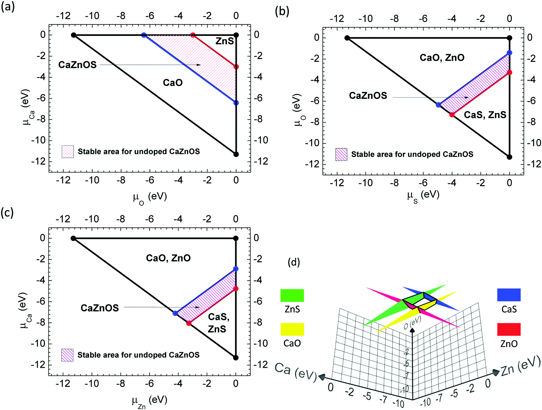 | ||
| Fig. 2 Calculated phase diagrams with respect to the chemical potentials of Ca (μCa), Zn (μZn), O (μO) and S (μS). | ||
| μ Ca | μ Zn | μ O | μ S | |
|---|---|---|---|---|
| Zn-rich | −3.04 | 0.00 | −6.28 | −3.00 |
| S-rich | −6.39 | −1.97 | −1.56 | 0.00 |
We found that the electronic states in the optical fundamental gap are less sensitive to the nonlinearity of Hubbard U parameters. Therefore, we used the Anisimov-type rotational-invariant DFT+U method.54 To minimize the effect of the localized hole states produced by the 2p orbitals of the O sites, the self-consistently determined Hubbard U potentials were also applied to the O-2p orbitals, which have reached a consensus55–58 in many oxide materials. Thus, it is necessary to consider both self-energy corrections on semicore orbitals for oxides.35,36,59
However, the non-self-consistently determined Hubbard U parameters usually induce an extra error in the lattice due to the non-zero residue of the second-order partial derivative to the charge density. It is necessary to consider our established self-consistent determination of the U parameters on the electronic structures35,36,52,58–60 in order to minimize the error in the lattice.
We chose the (3s, 3p, 3d, 4s) states as the valence states of Ca, (3d, 4s, 4p) for Zn, (3s, 3p) for S, and (2s, 2p) for O. We used OPIUM code in the Kleinman–Bylander form of norm-conserving pseudopotential61 with non-linear partial core correction62 to minimize the systematic error due to overlap of the atomic core-valence electron densities. Further, the RRKJ method was chosen to optimize the basis sets and the ionic minimization of the pseudopotentials.63 The norm-conserving pseudopotential was chosen because it can reproduce the all-electron behavior for outer shell valence electrons with |S-matrix| = 1 compared to ultrasoft pseudopotentials.64,65 As all of the constituent elements (Ca, Zn, S, and O) are light elements, the spin–orbit coupling effect was not implemented over the calculations. The kinetic cutoff energy was 850 eV, which expands the valence electron states in a plane-wave basis set. To prevent the charge-spin out-sync sloshing effect and guarantee the electronic minimization and convergence, the ensemble DFT (EDFT) method of Marzari et al.66 was used to solve the Kohn–Sham equation. The reciprocal space integration was performed by k-point sampling with a grid of 10 × 10 × 4 k points in the Brillouin zone of the CaZnOS unit cell, and a grid of 3 × 3 × 2 for defect electronic structure calculations in supercells. We further selected the (1/4, 1/4, 0) special k-point67 in the simple cubic 3 × 3 × 1 supercell. This converges the total energy to under 5.0 × 10⁻⁷ eV per atom. The Hellmann–Feynman force on each atom was converged to lower than 0.01 eV Å−1. The geometry optimization used the Broyden–Fletcher–Goldfarb–Shannon (BFGS) algorithm through all bulk and defect supercell calculations.
Another key setting is the pseudopotential for Ca. We generated the norm-conserving pseudopotential orbitals of 3s23p64s2 for Ca using OPIUM code. The 3d0 configuration was also considered in the generation. This does not change the valence distribution but will increase the accuracy of the valence electron interaction of Ca. In real DFT calculations, the 3d0 and 4s2 orbitals of Ca will have a certain overlap with an occupancy of 0.4 to 0.5 e through Mulliken analysis. This led us to consider an on-site Hubbard U energy reserved for this fractionally occupied empty 3d orbital for Ca. This consideration of 3dδ (0 < δ < 1) is also verified in the electronic structure calculations and experiments for CaB6, which is a new semiconductor for spin electronics.68–70 In that compound, the structure shows that the 3d orbital of Ca is hybridized with the 2p orbitals of the anions, affecting the band gap size of the Brillouin zone.71 For the total plane wave basis set for Ca, we used 850 eV, which was suggested by Clark et al. for similar norm-conserving generations.72 With our self-consistent determination process,33–36,52,53,59 the on-site Hubbard U parameters are 2.50 eV and 13.45 eV for the 3d orbitals of Ca and Zn, respectively, 2.87 eV for 3p of S, and 3.44 eV for 2p of O.
To calculate the defect formation energies at different charge states (q), we consider that the overall supercell was established and remained constant, based on the ground state relaxed primitive cell, to avoid the thermodynamic effect of enthalpy changes by cell variations. The formation energy of a targeted defect (Hq) at the specific charge state q can be described as a relationship of the positions of Fermi energy (EF) and the chemical potential Δμ of species with defects α, which is shown as follows:
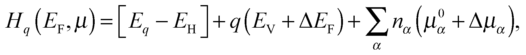 | (4) |
Results and discussion
Bulk CaZnOS
The crystal lattice of CaZnOS with a space group of P63mc has been studied by many groups. It was initially obtained by Sambrook et al. through the synthesis of CaCO3 (decomposed to CaO) and ZnS (reaction of Zn metal and S).47 It is noncentrosymmetric, like wurtzite ZnO, and its topology seems to be formed by similar compositions of CaO and ZnS in the forms of two puckered hexagonal layers, respectively. It is reported that the structure has good applications in piezoelectric luminescence and excellent second harmonic generation (SHG) capabilities due to the polar properties that are intrinsically induced by its noncentrosymmetric lattice symmetry.47,74 We recall that wurtzite ZnO has the same symmetry space group as P63mc. The 4-fold tetrahedral coordination of both the Zn and O sites in ZnO results in this noncentrosymmetric structure; consequently, ZnO possesses intrinsic piezoelectricity and pyroelectricity. This feature further induces a polar surface in ZnO; the most common polar surface is the basal plane, like ZnO (0001), which has been widely studied.53,75,76 Therefore, we can have a preliminary understanding of the piezoelectric properties of CaZnOS, and its coefficient is found to be three times larger than that of wurtzite ZnO.47The crystal lattice parameters of synthesized CaZnOS were found to be a = 3.76 Å and c = 11.40 Å.47 The relaxed structure of the ground state by our DFT+U calculation shows lattice parameters of a = 3.76 Å and c = 11.52 Å, with a very small error of 1%. Electronically, it has wide band gap semiconductor behavior, with a direct gap of 3.71 to 4.16 eV. From Fig. 3, the electronic band structure calculations based on the optimized cell give a direct band gap of 3.895 eV, which is very close to the data of 3.88 eV by the diffuse reflectance spectrum experimentally measured by Zhao et al.30 This calculated optical fundamental band gap is larger than the value of 3.71 eV found by Sambrook et al.,47 close to that of 4.0 eV found by Hintzen et al.,77 and much lower than that of 4.16 eV found by Wang et al.11 Therefore, our DFT+U calculation with ab initio-determined Hubbard-U parameters for fully-occupied Zn 3d10, as well as the p orbitals for the S and O sites, are self-consistent and reliable, as has also been illustrated in our previous work.33–36,52,53,59,78
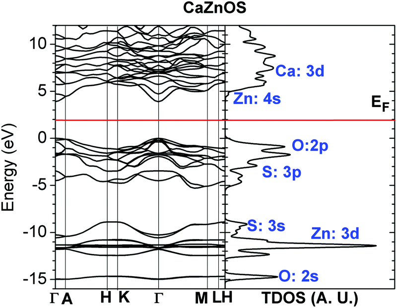 | ||
| Fig. 3 Band structure and total density of states (TDOSs) of CaZnOS. | ||
Fig. 3 also shows the orbital components of CaZnOS in TDOS. We can see that the top of the valence band consists of levels from the O-2p and S-3p orbitals. The lower conduction band is contributed by the Zn-4s and Ca-3d orbitals. The Zn-3d fully occupied level (3d10) is overlapping with the S-3s filled orbitals and remains in nearly the same energy range, while the O-2s orbital level remains lower.
Currently, due to the lack of available valence band X-ray photoemission spectrum data (XPS) for CaZnOS by experiment, we can only compare the qualitative trend result with BaZnOS, which has a similar chemical trend to CaZnOS. As we know, the optical fundamental band gap between CaZnOS (3.71 eV)47 and BaZnOS (3.91 eV)79 has a relatively small difference. Clarke et al. have performed a combined study of DFT calculations and XPS measurements on BaZnOS.79 In their valence band measurement, the top valence band is contributed by the O-2p and S-2p orbital levels and covers the related valence band width of about 6 eV below the VBM (valence band maximum) and above the t2g component of Zn-3d10. The repulsion between t2g of the Zn-3d10 and O-2p levels is usually underestimated in LDA and overestimated by hybrid functionals. Therefore, the band gap of 4.5 eV for BaZnOS estimated by Clarke et al. is overestimated by B3LYP. From the measured valence XPS, the peak of Zn-3d10 is located around 10 eV below the VBM in the BaZnOS system.79 From our calculated band structure and density of states, the Zn-3d10 level is at about 11 eV below the VBM, in good agreement with the trend found by XPS experiments.79
In the last section of this paper, we will also compare the X-ray diffraction (XRD) data between our simulated defective structures and experimentally synthesized samples (from two different groups). This will more clearly demonstrate the influence of the defects in the structure found by XRD.
For the bulk formation enthalpy of crystal CaZnOS, we have already shown that the calculated formation enthalpy of CaZnOS is −11.29 eV in the Experimental section, considering eqn (2) and (3).
S vacancy (VS)
The local structure of the S sites in the lattice is 6-fold coordinated, with 3 long S–Ca bonds with bond lengths of 3.036 Å and 3 short S–Zn bonds with lengths of 2.382 Å, 0.4% longer than the experimental data.47 The VS in the neutral state left two electrons bounded at nearby cation sites, such as Ca, Zn, or both. We accordingly studied its three different charge states (0, +1, and +2).Fig. 4(a) shows the TDOSs of CaZnOS with VS in the 0, +1, and +2 states. We can see that it is a deep donor-like trap center for V0S in CaZnOS. We found that the behaviors of the defect levels are very different from the VS in CaS based on our previous work.33 The formation of V0S-induced lattice relaxation gives two localized hole states next to the nearby cation sites, 0.35 eV and 0.72 eV below the CBM, respectively. The localized electronic defect levels of V0S show antiferromagnetic (AFM) behavior with 2.22 eV below the lowest localized hole state, which also denotes the highest occupied level (0 eV in Fig. 4(a)) of the system. For the V+S, there are five localized hole states with ferromagnetic (FM) behavior in the band gap. The spin-up hole states are 0.31 eV and 0.60 eV below the CBM, respectively. The third hole state is spin-down next to the localized electronic state (0 eV), with energy intervals of +0.76 eV. The remaining hole states (the fourth and fifth) are 0.17 eV and 0.50 eV below the CBM with spin-down, respectively, and are similar to the hole states with spin-up next to the CB edge. The localized electronic state given by V+S is 1.86 eV below the lowest localized hole state. For the V2+S in CaZnOS, there are only two pairs of spin-aligned levels with an energy interval of 0.95 eV with the highest hole levels 0.16 eV below the CBM, where the VBM acts as the highest occupied level (0 eV) under the +2 charge state.
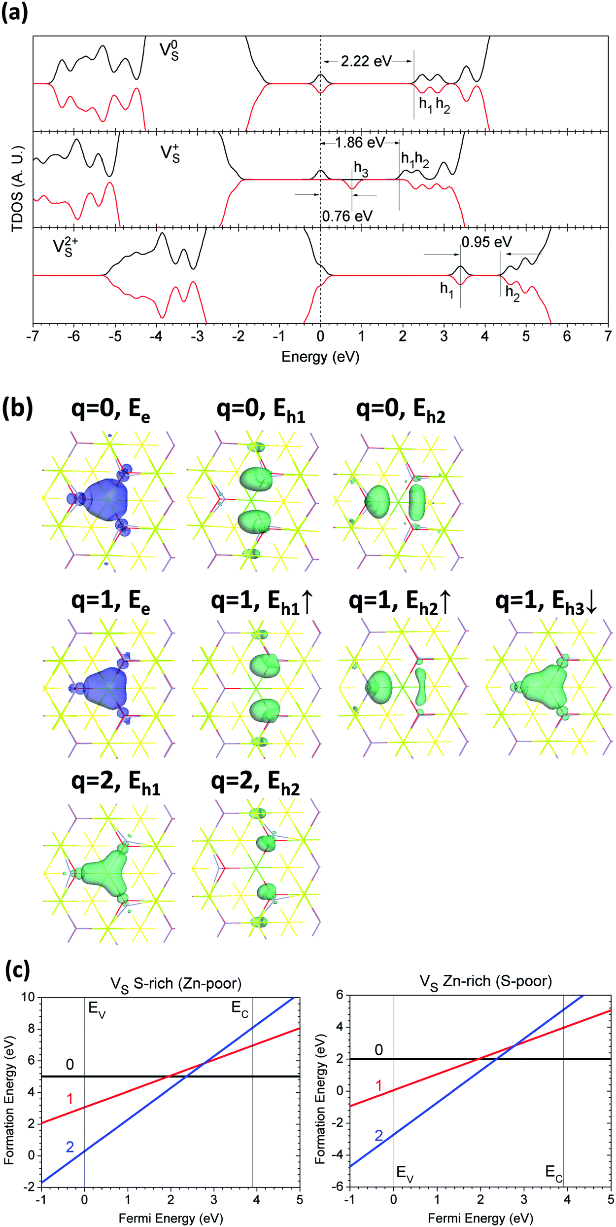 | ||
| Fig. 4 (a) TDOSs of VS in neutral (V0S), singly positive (V+S), and doubly positive (V2+S) states. The dashed line denotes the highest occupied level for electrons. (b) Localized electron and hole orbitals at the relaxed VS site (Zn = gray, O = red, S = yellow, Ca = green). (c) Formation energies of VS under S- and Zn-rich chemical potential limits. | ||
Fig. 4(b) shows the orbitals for localized electrons and holes that are induced by the VS in CaZnOS. We see that the local lattice relaxations at the ground state around the VS in different charge states are very different. This is rather evident in charge states 0 and +2, which are attracted to each other and repulsed by each other, respectively, as they move forward. Within the ground state, we confirm that the localized electrons left by VS are indeed localized at the nearby Zn sites instead of the Ca sites. Meanwhile, the electronic state is shared within the three Zn sites in both the V0S and V+S states. However, the localized hole states are spin-polarized and are found be complicated when given by VS, especially in V+S. This scenario is rather different from our previous work on the VS in CaS33 and from other similar anion vacancies, such as VO in oxides.34,35 The first hole state below the CBM remains at two Zn sites and the second hole below the CBM localizes on a Zn site, sharing between the other two Zn sites (for either V0S or V+S). The third hole given by V+S in the spin-down state is shared between the three Zn sites. V2+S induces two types of localized holes which have similar orbitals to V0S and V+S. These as-shown localized hole states arise because of the local distortions of Zn-sites induced by the perturbed hole states (PHS) next to the CB edge.80,81
The formation energy calculation in Fig. 4(c) shows that the S vacancy (VS) in CaZnOS possesses negative effective correlation energy (negative-Ueff) of −0.84 eV, which is exothermal for the defect reaction process of 2V+S → V0S + V2+S and is nearly undetectable by ESR measurement at a realistic concentration. This implies that the dominant charge states of VS in CaZnOS are 0 and +2. The V+S state can temporarily exist in the host lattice due to external UV photo-irradiation or other excitations. The neutral state V0S has formation energies of 5.01 eV and 2.01 eV under S-rich and Zn-rich chemical potential limits, respectively. The thermodynamic transition level of VS is 2.36 eV for (0/2+) above the VBM, which indicates that it is a deep donor-like trap center that binds the two localized electrons left by neutral V0S. Accordingly, VS here is unlikely to be a F-center, as F+ does not stably exist in the host lattice, due to the evident lattice relaxations of neighboring Zn sites given by negative-Ueff.
O vacancy (VO)
Fig. 5(a) shows the TDOSs of CaZnOS with VO in the 0, +1, and +2 states. We find that it is also a deep donor-like trap center, and it is slightly deeper than VS. This may arise because the localized hole states ascend toward to the CBM or because the Coulomb repulsive potentials between localized electrons and the CB edge states become stronger. We see that the local lattice relaxation given by V0O induces six localized hole states that are spin-paired near the Ca and Zn sites, overlapping with the CBM; these are more than the states observed in VS. These three pairs of localized holes are 0.15 eV, 0.22 eV, and 0.49 eV below the CBM. The localized electronic states left by neutral VO (V0O) in CaZnOS are 2.46 eV below the CBM, with similar AFM behavior. V+O ionizes one electron out from the site and produces one extra localized hole state; meanwhile, the left electron is localized 2.90 eV below the lowest localized hole state. This is different from the case of V+S, as V+O has an electronic state 0.54 eV further away from the CBM, while V+S is 0.36 eV further away, which is much closer to the lowest localized hole level. Three of the subsequent four localized hole states induced by V+O are 0.20 eV, 0.30 eV, and 0.45 eV below the CBM, respectively. The fourth one, in the spin-down state, has energy intervals 1.15 eV higher than the localized electronic level. The remaining three localized hole state levels are 0.14 eV, 0.25 eV, and 0.52 eV below the CBM, respectively, in the spin-down state. For V2+O, there are only two pairs of spin-aligned levels, with an interval of 1.47 eV, and the highest localized hole levels are 0.26 eV below the CBM. This arises because V2+O ionizes all of the electrons, and three localized hole states degenerate into a triplet state next to the CB edge.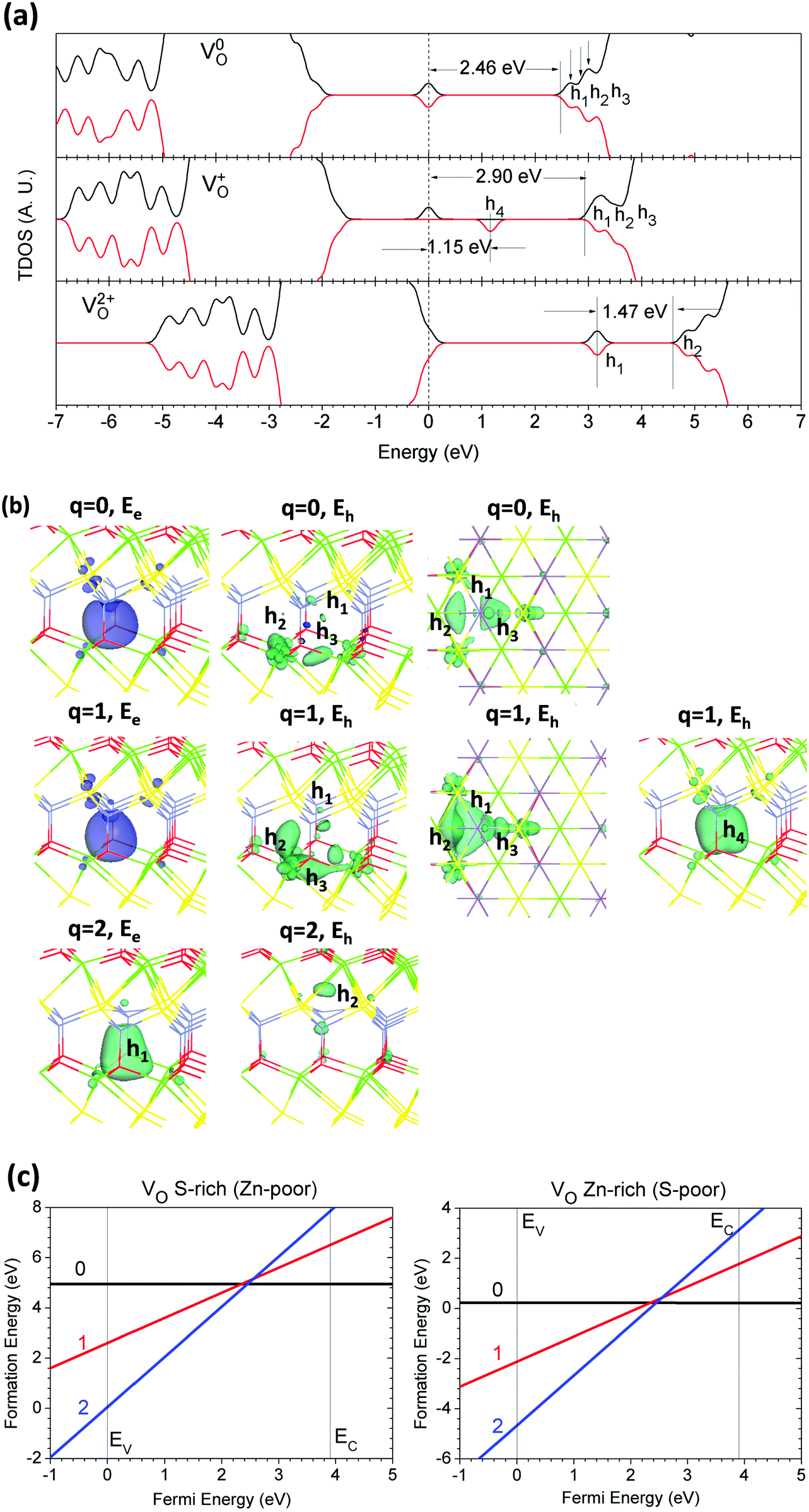 | ||
| Fig. 5 (a) TDOSs of VO in neutral (V0O), singly positive (V+O), and doubly positive (V2+O) states. The dashed line denotes the highest occupied level for electrons. (b) Localized electron and hole orbitals at the relaxed VO site with side and top views (Zn = gray, O = red, S = yellow, Ca = green). Note that h1, h2, and h3 are combined in the same figure; actually, they present independently to each other based on their own orbital levels. (c) Formation energies of VO under S- and Zn-rich chemical potential limits. | ||
Fig. 5(b) shows the localized orbitals of localized electrons and holes induced by VO in the relaxed host lattice. The relaxations on the Zn site at 0 and +2 are more obvious than those on the Ca sites near the VO site. The relaxed Zn site moves downward to the center of the VO site. The localized electrons left by V0O are localized around the Zn site and the three Ca sites. The three localized holes are mainly distributed around the three Ca sites, except the first hole, which remains at the distorted Zn site. The second hole is shared by two Ca sites, while the third hole is shared by three Ca sites, respectively. In the case of V+O, the electronic orbital is similar to that of V0O with slight distortion, and the Zn site has almost no relaxation. The three localized holes have nearly the same distribution as in V0O, while the second hole is shared between two Ca sites and the Zn site. The deeper fourth hole remains near the center of VO, shared between three Ca sites and the Zn site. For V2+O, the first localized hole also remains at the center of VO, while the second hole near the CBM only sits at the Zn site and acts like a back-bonding orbital.
The formation energy of VO, shown in Fig. 5(c), shows that it is also a negative-Ueff defect, with −0.20 eV. This indicates that VS in the host lattice has only 0 and +2 as the dominant charge states, similar to VS. The formation energies of neutral VS are 4.95 eV and 0.23 eV under the S-rich and Zn-rich chemical potential limits, respectively. We found that under the S-rich limit, the formation energies of VO and VS are nearly the same, while VO is much lower than VS (0.23 eV vs. 2.01 eV) under the Zn-rich limit. This indicates that VO is more easily formed than VS, even under S-poor chemical conditions, and is more dominant as a native point defect in the CaZnOS lattice. The thermodynamic transition level is 2.45 eV for (0/2+) above the VBM, which is also a deep donor trap for the localized electrons at the V0S site. Thus, VO has similar electronic behavior to VS; however, it induces more localized hole states. Moreover, it cannot be the F-center because the formation of F+ has a higher energy cost.
Interstitial S (Si)
As we know, there are many possible sites where excess S can act as an interstitial in the CaZnOS host lattice, as well as O interstitial defects, which we will discuss in the following section. This arises because the local structures are very different from the conventional ZnS or ZnO structures, as analyzed by Sambrook et al.47 Considering the lattice character, we examined five possible Si sites in CaZnOS. These sites may act as acceptor traps to capture electrons and release holes.Fig. 6(a) shows the TDOSs of the five Si in CaZnOS in the neutral state (S0i). We can see that they have almost identical TDOSs. Their localized electronic states are about 0.2 eV higher than the VBM and 0.4 eV below the CBM for the localized holes. Further formation energy calculation shows that Si3 has the lowest formation energy in the neutral state (S0i3).
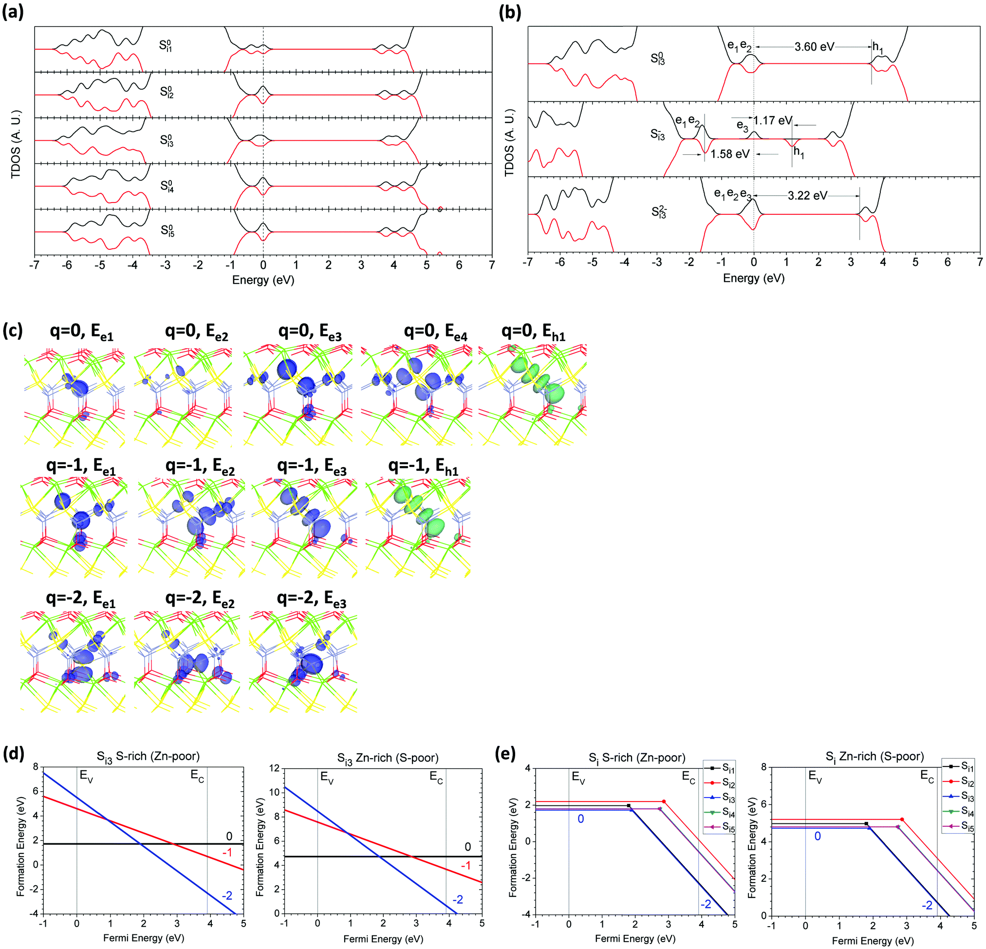 | ||
| Fig. 6 (a) TDOSs of five possible Si sites in the neutral (S0i) state. (b) TDOSs of Si3 in neutral (S0i3), singly negative (S+i3), and doubly negative (S2+i3) states. The dashed line denotes the highest occupied level for electrons. (c) Localized electron and hole orbitals at the relaxed Si3 site with side and top views (Zn = gray, O = red, S = yellow, Ca = green). (d) Formation energies of Si3 under S- and Zn-rich chemical potential limits. (e) Summary of the formation energies of five possible Si sites under S- and Zn-rich limits. | ||
Fig. 6(b) illustrates the TDOSs of Si3 in charge states of 0, −1, and −2. In the neutral state, there are four localized electronic states, two of which overlap, with an interval of 0.21 eV from peak to peak. The highest localized electronic state remains at 0.68 eV higher than the VBM and 3.60 eV below the localized hole state, while the hole sits 0.26 eV below the CBM. For S−i3, an excess electron remains 1.58 eV higher than the previous two localized electronic states, while the previous two electronic states are almost fixed to a position 0.68 eV higher than the VBM. The excess electron also induced an empty state (hole level) with an interval of 1.15 eV. For S2−i3, two excess electrons terminate the excess hole level near the mid-gap and show three overlapping localized electronic states with 0.03 eV and 0.24 eV as intervals, respectively. The lowest electronic level is 1.16 eV higher than the VBM.
Fig. 6(c) shows the orbitals of localized defect levels induced by Si3 in CaZnOS. As we know, the anion interstitial defect in sulfides or oxides usually forms a local peroxide structure. We can see from Fig. 6(c) that the S interstitial (Si) induces evident lattice relaxation and reconstruction near the Si3 sites, with formation of a homopolar S–S bond. The p–π orbitals localize along this S–S bond, induced by the relaxed Si site at the ground state. S0i3 in CaZnOS has two localized electronic states, which are spatially distributed between two S sites connected by S–S bonds, respectively. The localized hole level arises from the p–π* antibonding orbital longitudinally along the S–S bond. S−i3 induces different local lattice distortions as strong electron–lattice coupling. The electronic orbitals become polarized along the distorted lattice sites. The localized electronic and hole states within the mid-gap area have nearly the same orbitals, showing a strong coupling effect for these polarons. For S2−i3, it can be seen that the two captured electrons are localized at the Si3 site itself. The two excess electrons which have been captured and localized actually generate three different localized p–π orbital components on the Si3 site, with a slight distribution on nearby S and O sites.
The formation energies of S0i3 in CaZnOS are 1.73 eV and 4.73 eV respectively under the S-rich and Zn-rich chemical potential limits, as shown in Fig. 6(d). S0i3 shows a negative-Ueff behavior with −1.97 eV. The transition level of the state (2−/0) of Si3 is 1.89 eV above the VBM. This indicates a deep acceptor trap whose level is at the mid gap. We find that all of the S interstitial defects present similar strong electron–lattice coupling effects with negative-Ueff within the range of −0.23 eV to −1.97 eV, as shown in Fig. 5(e). We further illustrate the related transition levels distributed within the range of 1.80 to 2.86 eV above the VBM.
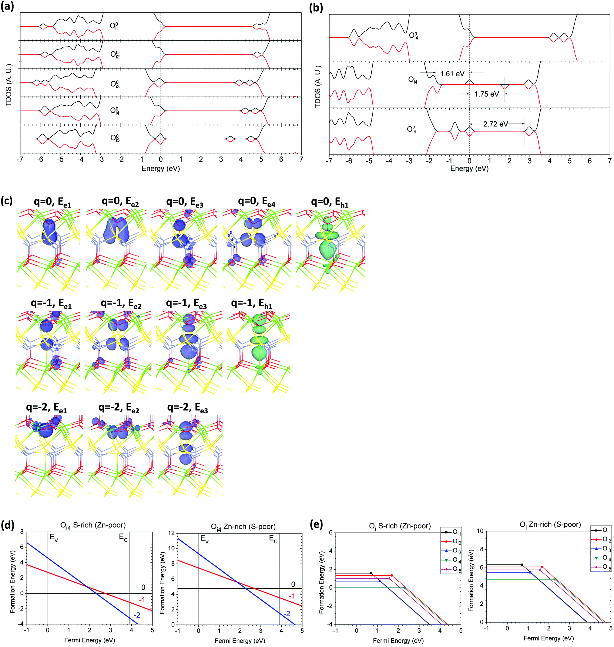
Interstitial O (Oi)
Oi in CaZnOS within different local bonding and charge states actually induces more complicated localized electronic and hole states coupling with nearby lattice sites than interstitial S. As illustrated in previous studies, Oi in metal oxides such as CeO235 and Er2O334 forms peroxides with O–O homopolar bonds, which localizes π-electrons along these bonds surrounding the Oi site. Here, we find that an S–O bond is formed for some Oi, depending on the different local positions of interstitial O.As shown in Fig. 7(a), in the neutral state of Oi, the occupied defect levels remain closer to the VBM than in Si. Other localized levels sit 5.8 to 6.2 eV below the VBM. The localized hole levels remain deeper or shallower, from 0.2 eV to 1.0 eV, in contrast to the states produced in Si. By calculating the formation energies, Oi4 is most likely to form because it has very low formation energy, where Oi is surrounded by three Ca sites and one S site. This strong Ca–O bonding leads to an evident relaxation process which is nearly spontaneous and provides local stabilization.
 | ||
| Fig. 7 (a) TDOSs of five possible Oi sites in the neutral (O0i) state. (b) TDOSs of Oi4 in neutral (O0i4), singly negative (O−i4), and doubly negative (O2−i4) states. The dashed line denotes the highest occupied level for electrons. (c) Localized electron and hole orbitals at the relaxed Oi4 site with side and top views (Zn = gray, O = red, S = yellow, Ca = green). (d) Formation energies of Oi4 under S- and Zn-rich chemical potential limits. (e) Summary of formation energies of five possible Oi sites under S- and Zn-rich limits. | ||
Fig. 7(b) shows that in the neutral state of Oi4, there are four localized electronic states; three remain near the top of the VB, about 0.31 eV higher than the VBM, while the fourth state is below the VB. The total weighted area is about 6.3 localized electrons, which is consistent with the six total electrons induced in the host lattice produced by the O interstitial defect. The O−i4 in the lattice has a clear localized hole state in the band gap, 1.75 eV higher than the localized electronic state or 3.36 eV above the VBM. The other occupied electronic states are localized near the VBM, about 0.2 eV higher. The localized VB edge states show minor ferromagnetic behavior with spin-polarization. The O2−i4 in the lattice shows that all of the excess electronic states are localized within the band gap, 0.90 eV and 1.63 eV higher than the VBM.
Fig. 7(c) shows the orbitals of localized electronic and hole levels (occupied and unoccupied, respectively) within different charge states for Oi. The electronic orbitals localized along the O–S bond present a coupled π-orbital for the state below the VBM, while the VB edge states show two individual localized π-orbitals with two different directions. The localized hole state of O0i4 gives hybridized orbitals between dz2 and p–π orbital components from Ca and S sites, respectively. In the O−i4 state, the O–S bond has been broken and has pushed the S site downward to form a vertical Ca–S bond. The p–π orbitals become more localized individually on the Oi and S sites, with two different directions; meanwhile, the localized hole states are redistributed vertically along the Oi–S–Ca bonds. The O2−i4 in the lattice has three different localized electronic states; two are localized between Oi and three Ca sites with an O–Ca bond. The third one produces weak π–π coupling given by the p–π orbitals of the Oi and S sites, respectively.
We consider the formation energy of Oi, shown in Fig. 7(d) and (e). We found that Oi4 has formation energies of 0.02 eV and 4.74 eV under the S-rich and Zn-rich limits. The thermodynamic transition level of (2−/0) of Oi4 is 2.29 eV above the VBM and acts as a deep acceptor trap center in the lattice. In Fig. 6(e), we show that all of the possible Oi sites in the lattice present negative-Ueff effects. We found that the transition level of (2−/0) varies from 0.70 eV to 2.29 eV above the VBM, dependent on the positions of Oi. This shows that Oi4 is energetically favorable to localize and stabilize within the cage of (3Ca + S), where the strong Ca–O bonds will enhance the charge transfer to stabilize the system. It is also consistent that O has relatively small ionic radii compared to S. Thus, it costs less energy for O to penetrate the ideal lattice and stabilize near the Ca and S sites.
Calcium vacancy (VCa)
We turn to cation-related defects. We firstly studied the Ca vacancy (VCa). The neutral VCa in CaZnOS (V0Ca) left two localized holes occupying nearby O-sites. This arises because the formation of a cation vacancy normally induces electron–hole separation while suppressing the occupied electronic states downward to lower energy levels, simultaneously resulting in localized hole states within the band gap.The single particle levels in the form of TDOSs are shown in Fig. 8(a), which confirms the deep localized hole trapping levels at about 1.68 eV above the VBM, which are both spin-down. These holes mainly occupy the p-orbitals of nearby O-sites. Due to the relaxation of O-sites near the VCa, the strong coupling between p-electrons and the lattice will also affect the occupied p-orbital levels and the consequent redistribution of the orbital charge densities near the defect sites and relaxed lattices. There are six localized electronic states; two remain 5.4 eV and 5.6 eV below the VBM, while the other four states remain 0.06 eV, 0.11 eV, 0.28 eV, and 0.32 eV above the VBM, respectively. For the V−Ca in the lattice, one of the localized hole states was released by capturing an electron. The remaining holes are localized 1.57 eV above the VBM. Due to the local lattice relaxation, the p-orbital levels on the local under-coordinated S and O sites are re-aligned, as shown in Fig. 8(a). We can see that one of the low-lying p-orbital levels is pushed to the highest occupied state, and the occupied levels above the VBM are updated as 0.07 eV, 0.08 eV, 0.28 eV, 0.32 eV, and 0.36 eV, respectively. Through further passivation of the hole, the V2−Ca in the lattice pushed all of the localized p-orbitals on the nearby S and O sites toward the highest occupied range above the VBM, with energy intervals of 0.06 eV, 0.08 eV, 0.24 eV, 0.28 eV, 0.34 eV, and 0.38 eV, respectively.
 | ||
| Fig. 8 (a) TDOSs of VCa in neutral (V0Ca), singly negative (V−Ca), and doubly negative (V2−Ca) states. The dashed line denotes the highest occupied level for electrons. (b) Localized electron and hole orbitals at the relaxed VCa site (Zn = gray, O = red, S = yellow, Ca = green). (c) Formation energies of VCa under S- and Zn-rich chemical potential limits. | ||
Fig. 8(b) shows the localized orbitals of the corresponding defect states induced by the VCa in the lattice at different charge states. We illustrated that both the positions and directions of the localized electronic orbitals are varied at the different energy levels discussed above. At the neutral charge state, two localized holes individually remain at the p-orbitals of the under-coordinated O sites neighboring VCa. Similarly, V−Ca shows a single hole state localized on one of the O sites near the VCa. The localized electronic orbitals present subtle electron–lattice coupling at different energy levels. We found that some states about 3.2 eV below the VBM induced differences in the TDOSs; however, we did not observe any localized orbitals.
The formation energies of the VCa in the lattice within different charge states are shown in Fig. 8(c). The neutral state of VCa (V0Ca) costs 3.88 eV and 7.22 eV under the S-rich and Zn rich limits, respectively. It has a very small negative-Ueff effect of −0.05 eV. This arises because the transition levels between the states of (2−/−) and (−/0) are very close. Meanwhile, the degrees of lattice relaxation near VCa within three different charge states (0, +1, and +2) are nearly the same. The thermodynamic transition level of the state (2−/0) locates inside the VB, which is 0.51 eV below the VBM, or EV − 0.51 eV (EV = 0 for VBM). This indicates that the trap level of the VCa, acting as an acceptor trap, is buried in the VB, which releases the free holes.
Zinc vacancy (VZn)
The Zn vacancy (VZn) in the lattice induces more complicated electron–hole separation and interactions. The local lattice geometry is different from the VCa in the lattice due to the different local coordinations between the Zn and Ca sites. VZn only has three Ca sites and one O site nearby. Thus, the localized electronic state arrangement is different and degenerates, as the number of under-coordinated O-sites is lower than that in the case of VCa.The TDOSs of CaZnOS with VZn have some differences compared with the lattice with VCa. As shown in Fig. 9(a), there are two localized hole states within the band gap in the neutral state (V0Zn), 1.22 eV and 2.19 eV above the VBM, respectively. Their spin states are all spin-down and un-paired. There are five localized electronic states induced by the relaxed lattice near the VZn; three are 5.05 eV, 3.37 eV, and 3.27 eV below the VBM, while two are 0.16 eV and 0.20 eV above the VBM. For the V−Zn in the lattice, the alignment of the localized electronic states is nearly unchanged; three are 5.46 eV, 3.59 eV, and 3.55 eV below the VBM, and two are 0.16 eV and 0.50 eV above the VBM. We can also see that the electronic states above the VBM become more localized toward the levels deep in the gap. One of the localized hole states is released, and the other one remains at 1.74 eV above the VBM. The scenario is more evident in the TDOS of CaZnOS with V2−Zn; the localized electronic states remain above the VBM, with energy intervals of 0.09 eV, 0.15 eV, 0.21 eV, 0.50 eV, and 0.63 eV, respectively.
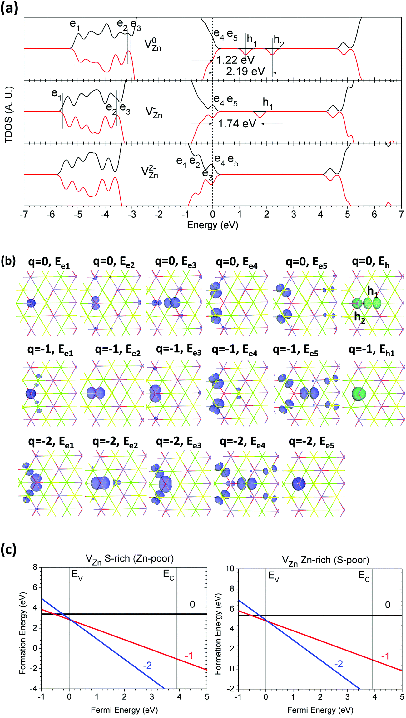 | ||
| Fig. 9 (a) TDOSs of VZn in neutral (V0Zn), singly negative (V−Zn), and doubly negative (V2−Zn) states. The dashed line denotes the highest occupied level for electrons. (b) Localized electron and hole orbitals at the relaxed VZn site (Zn = gray, O = red, S = yellow, Ca = green). (c) Formation energies of VZn under S- and Zn-rich chemical potential limits. | ||
We further examined the localized orbitals of the electronic and hole states given by VZn as well as the relaxed lattice sites, as shown in Fig. 9(b). We can see that the shallower localized hole state in CaZnOS with V0Zn is at the S site near VZn, while the 3-fold coordinated O site has another hole state deep in the mid-gap. In CaZnOS with V−Zn, the remaining localized hole state is localized near the mid-gap, with 0.45 eV movement toward to the VBM due to the Coulomb attractive potentials from localized electronic states at the relaxed lattice sites neighboring VZn.
The formation energy calculations of VZn in CaZnOS also show differences compared to VCa in the lattice. We can see from Fig. 9(c) that Ueff is positive (+0.61 eV). This arises because the local lattice sites have minor relaxation near VZn within different charge states. The thermodynamic transition levels of the states (−/−0) and (2−/−) remain at 0.54 eV below and 0.07 eV above the VBM, respectively. This indicates that VZn will cause the lattice to capture electrons and release free holes ranging from the top to deep inside the VB, which will continuously transport the free holes to the VB edge for excitation into or across the optical band gap.
Calcium interstitial (Cai)
Excess Ca in CaZnOS acting as an interstitial defect (Cai) may be a donor-like source center to release excess electrons into the lattice. Neighboring anion sites such as O and S will be vastly affected, resulting in bonding hybridizations and lattice reconstructions. The local distorted sites will also influence the electronic and hole states in the band gap or edges that accommodate the charge carriers.Fig. 10(a) shows that the neutral Cai (Ca0i) in CaZnOS induces an electronic state that is localized in the band gap 2.43 eV above the VBM. The Ca+i in CaZnOS in the lattice gives a localized hole state 0.53 eV below the CBM; the other localized electronic states remain 3.05 eV higher than the VBM. The Ca2+i in CaZnOS ionized two excess electrons and produced very shallow hole states that overlap with the CB edge, remaining right below the CBM.
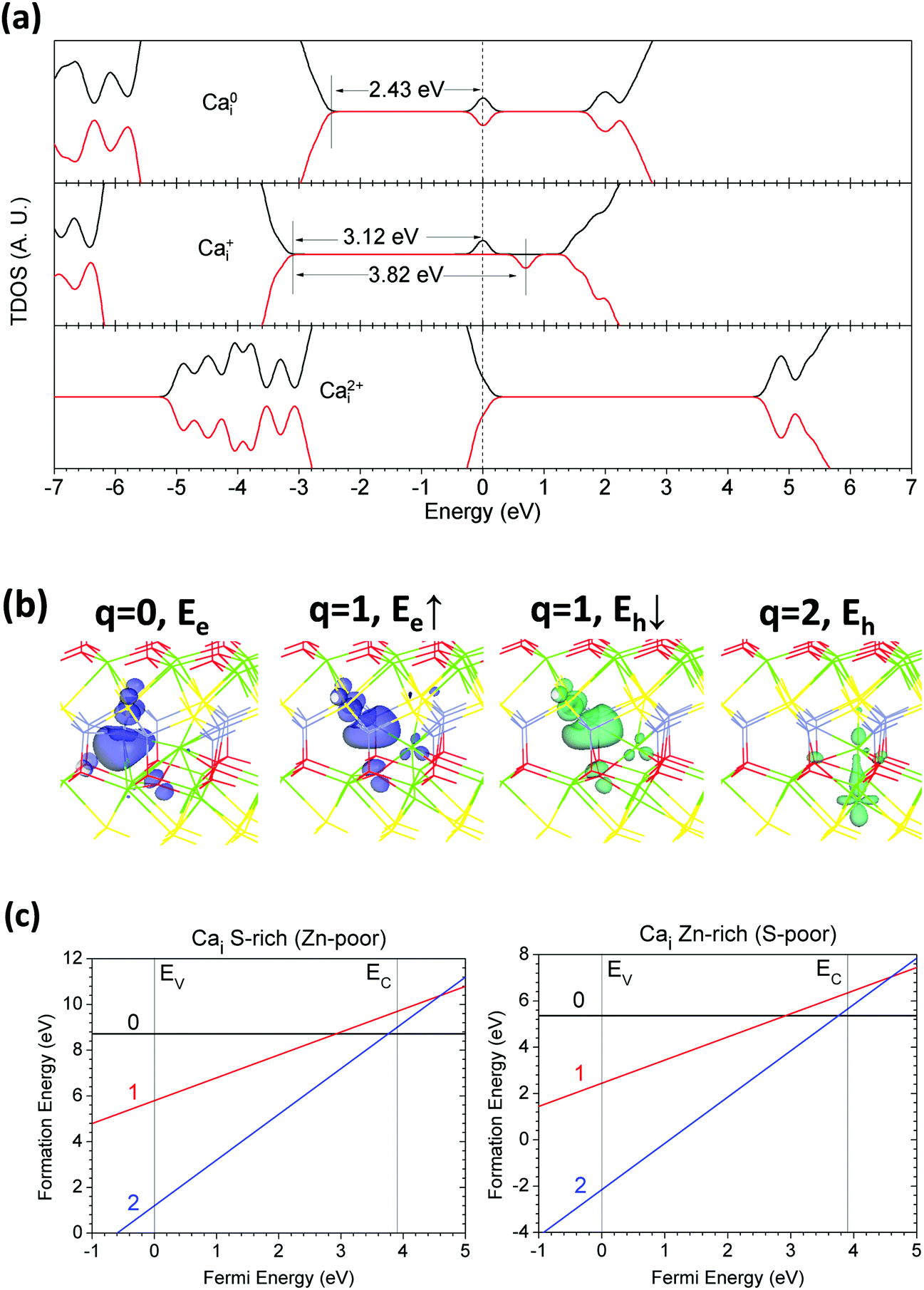 | ||
| Fig. 10 (a) TDOSs of Cai in neutral (Ca0i), singly positive (Ca+i), and doubly positive (Ca2+i) states. The dashed line denotes the highest occupied level for electrons. (b) Localized electron and hole orbitals at the relaxed Cai site (Zn = gray, O = red, S = yellow, Ca = green). (c) Formation energies of Cai under S- and Zn-rich chemical potential limits. | ||
We found that the Cai in the lattice induced relaxation, leading to a large displacement of the adjacent Zn site. The distorted Zn site shows electronic orbital localization at the 0 and +1 states, as shown in Fig. 10(b). The Ca2+i induced two localized hole states sitting on the Cai and adjacent Ca sites (from the lower layer). We can see that the hole orbitals consist of the d orbitals with components of hybridized dz2 and dx2−y2 remaining at the Cai sites. This arises because the 3d orbitals of Ca2+ ion are not ideally empty and partially overlap with other orbitals, acting like a d-acceptor center, as reported previously.33,71
For the formation energy calculation in Fig. 10(c), we see that the lowest formation energies of Cai among different possible local sites are 8.72 eV and 5.37 eV under the S-rich and Zn-rich limits, respectively. We also found that this interstitial defect also presents a negative-Ueff effect, with an energy of −1.68 eV. This arises because the incidence of Cai and results in vast lattice relaxation toward to the ground states at the charge states of 0 and +2. Therefore, Cai in CaZnOS only has two different possible charge states (0 and +2, respectively).
Zinc interstitial (Zni)
The Zn interstitial (Zni) in the CaZnOS lattice has slightly different electronic properties. As shown in Fig. 11(a), the TDOS calculation tells us that neutral Zni (Zn0i) induces additional electronic states localized in the band gap 2.74 eV above the VBM, while also providing localized hole states 0.20 eV below the CBM. The Zn+i in the lattice gives one shallow electronic state localized 1.00 eV below the CBM, with only one localized spin-down hole state remaining 0.59 eV below the CBM. The Zn2+ in the lattice does not provide any localized defect levels in the band gap, nor any localized hole states in the band gap or edges, as it ionized two excess electrons originating from the 4s2 orbital. Due to the fully-occupied 3d10 orbitals 0.30 eV below the VBM, Zn2+ is less likely to generate a d-acceptor center than the Cai in the host lattice.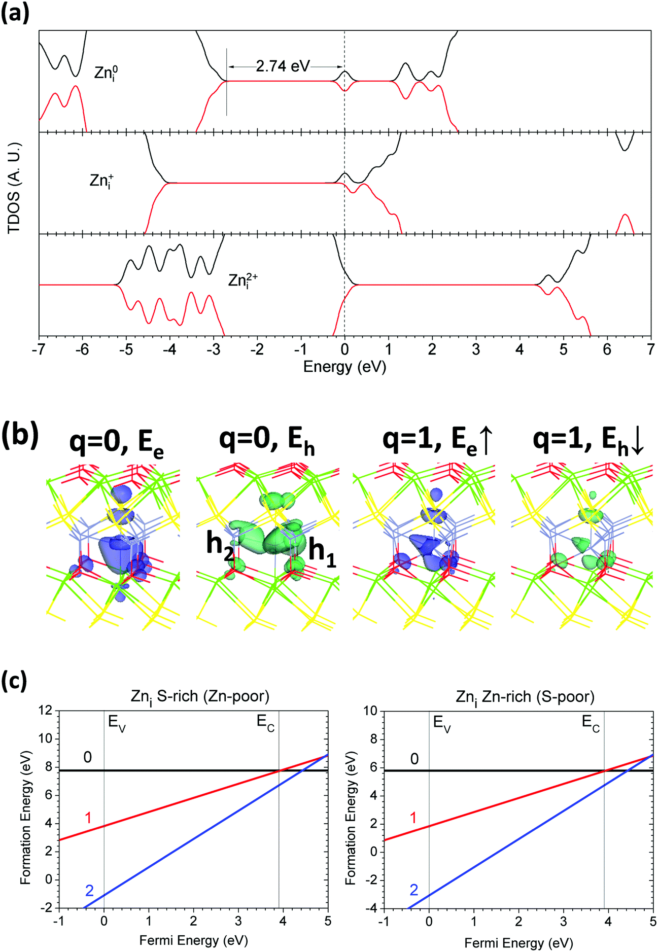 | ||
| Fig. 11 (a) TDOSs of Zni in neutral (Zn0i), singly positive (Zn+i), and doubly positive (Zn2+i) states. The dashed line denotes the highest occupied level for electrons. (b) Localized electron and hole orbitals at the relaxed Zni site (Zn = gray, O = red, S = yellow, Ca = green). (c) Formation energies of Zni under S- and Zn-rich chemical potential limits. | ||
Through further study of the localized orbitals, as shown in Fig. 11(b), we found that the localized electronic state at the neutral state is localized at the Zni site and spread vertically along the S–Zn–Ca bonds, which is mainly the sp orbital hybridization. We can also see that the two localized hole states remain along the Zn–Zn homopolar bond. For Zn+i, the localized electrons and holes remain at the Zni site. There is no orbital sitting at Zn2+i, as there are no localized states within the band gap at this charge state in the host lattice.
Zni has different formation energies when it is located in different lattice sites. As we found, the difference is as high as 1.77 eV. We can see from Fig. 11(c) that the lowest energy Zni in the lattice also presents a negative-Ueff behavior, showing a strong electron–lattice coupling, and the energy scale is about −0.48 eV. The lattice relaxation mainly occurs at Zni and the nearby Zn, S and Ca sites. The formation energies of Zn0i in the lattice are 6.01 eV and 4.04 eV under the S-rich and Zn-rich limits, respectively. The thermodynamic transition level of the state (0/2+) is 4.00 eV above the VBM, which actually slightly overlaps with the CB edge or is buried in the CB. This indicates that Zni is a possible donor-like center that readily releases free electrons. Due to the negative-Ueff effect, the possible charge states of Zni are 0 and +2 in the host lattice.
Anion Frenkel defects (a-Fr) and Schottky defects (STK)
Based on the aforementioned native point defects, we further examined the charge complementary pair defects, which are usually a class of lattice distortions induced by conditions of external thermal fluctuation. The dominant types of these defects are Frenkel (Fr) defects (including cation and anion Fr defects) and Schottky (STK) defects. Among these types of defects, the anion Fr (a-Fr) and STK defects are the main pair defects that affect the electronic and optical properties of CaZnOS. This arises because the cation Fr (c-Fr) requires more formation energy to generate the interstitial cation, as discussed above. Meanwhile, the formation energies of the cation vacancies are not primarily low compared with those of the anion vacancies. This may result from the differences in the ionic radii of the elements. For further consideration, two different kinds of a-Fr will be considered; one is O-related, while the other is S-related. Meanwhile, for the STK defects, we specified five different kinds, which are VZnO, VZnS, VCaO, VCaS, and VCaZnOS, respectively.We summarized the formation energies of these defects in neutral states under the S-rich and Zn-rich limits, as shown in Table 2. We found that in the a-Fr pair defects, the O related a-Fr has lower formation energy (2.39 eV per O defect site) than the S a-Fr (3.32 eV per S defect site), and these remain constant under both chemical potential limits. The VZnO has the lowest formation energy under the Zn-rich limit, which is 0.42 eV per defect site; this denotes the dominant type of defect under this chemical potential limit compared with the other pair defects. VCaZnOS also shows consistent formation energy, with 1.03 eV per defect site regardless of the different chemical potential limits, as it also contains the sub-component of VZnO. Therefore, we direct our focus on the electronic properties of VZnO in the following discussion.
| S-rich | Zn-rich | |
|---|---|---|
| a-Fr(O) | 2.39 | 2.39 |
| a-Fr(S) | 3.32 | 3.28 |
| VZnO | 1.79 | 0.42 |
| VZnS | 2.31 | 1.79 |
| VCaO | 2.13 | 1.44 |
| VCaS | 2.67 | 2.84 |
| VCaZnOS | 1.07 | 1.07 |
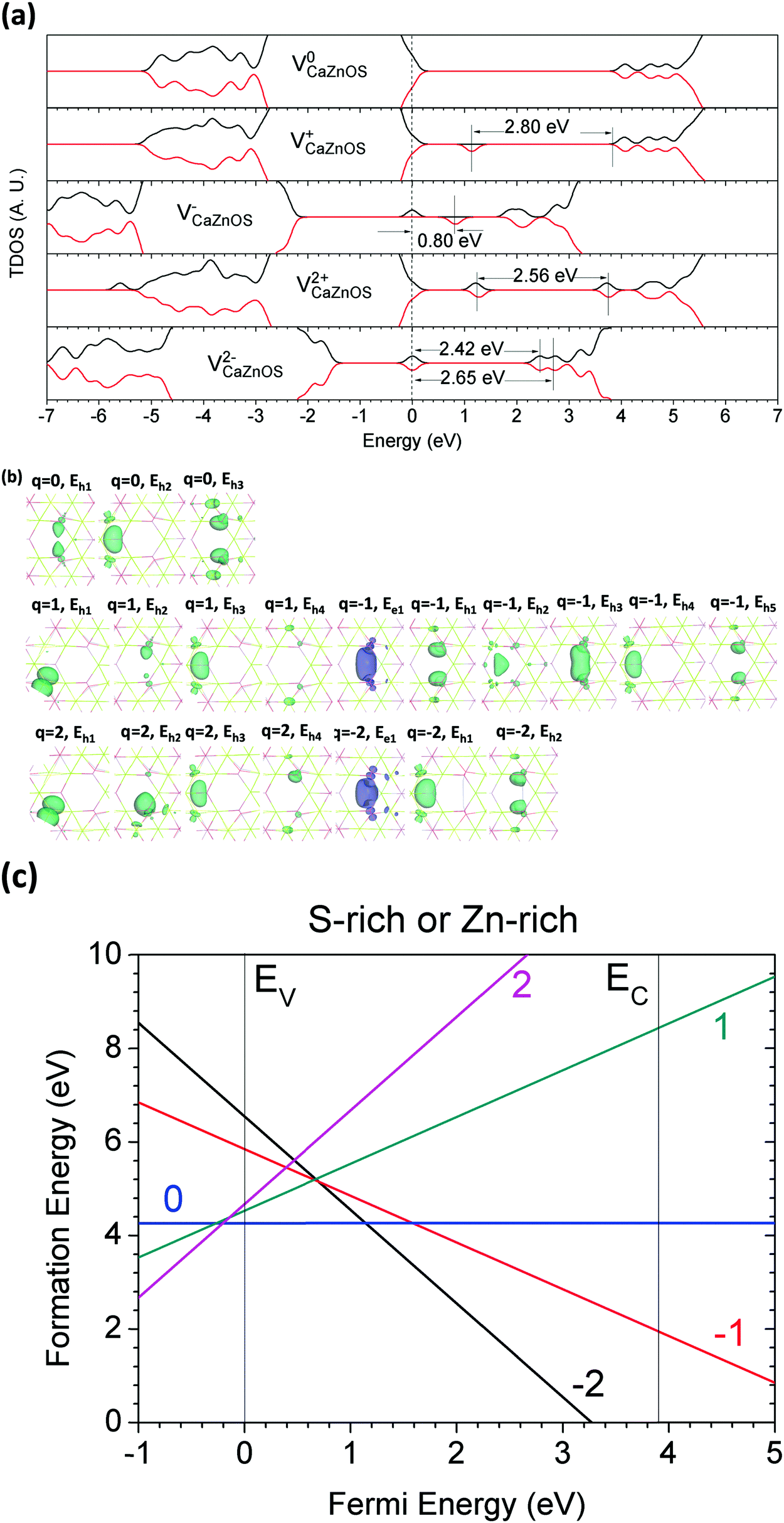
As shown in Fig. 12(a), we studied the TDOSs of five charge states of VZnO in the CaZnOS lattice (0, +1, −1, +2, and −2). V0ZnO in the lattice produces localized electronic and hole states with energy intervals of 3.24 eV, and the electronic level is about 0.2 eV above the VBM. In the V+ZnO state, an extra hole state is induced in the lattice, about 1.0 eV higher than the VBM, and the original localized hole states move toward to the CBM, with 0.3 eV. The energy interval between the hole states is 2.57 eV. In the V−ZnO state, the excess electronic state remains 2.60 eV above the VBM, and the CB edge states show ferromagnetic (FM) behavior. For the V2+ZnO state, two pairs of hole states are localized within the band gap area, with an energy interval of 2.50 eV. We recall that the intrinsic persistent luminescence of CaZnOS has a broad peak centered at 500 nm (2.48 eV). Thus, V2+ZnO accounts for the activator site of the intrinsic persistent luminescence. For the V2−ZnO state, two pairs of electronic states are localized within the band gap, with an energy interval of 3.54 eV. This arises because of the increased Coulomb repulsive potentials due to the increased electrons localized at the VZnO site.
 | ||
| Fig. 12 (a) TDOSs of VZnO in charge states of 0, +1, −1, +2, and −2. The dashed line denotes the highest occupied level for electrons. (b) Localized electron and hole orbitals at the relaxed VZnO site (Zn = gray, O = red, S = yellow, Ca = green). (c) Formation energies of VZnO under S- and Zn-rich chemical potential limits. | ||
Fig. 12(b) shows the localized orbitals of the electronic and holes states induced by the VZnO in the lattice. For the neutral state, the electronic and hole states remain at the interlayer under-coordinated S and Ca sites, respectively. In the V+ZnO state, the excess hole state remains at the one of the under-coordinated S sites, while the other states remain at the same sites. For the V−ZnO state, the excess electronic state surrounds the three under-coordinated Ca sites; the other orbitals remain at the same sites, with a slight distortion of the original hole state. For the V2+ZnO state, the localized hole states are located at the under-coordinated S and Ca sites. The lower energy hole state (close to the VBM) is at two of the three under-coordinated S sites, with spin-up and spin-down, respectively. The higher energy hole (close to the CBM) is low lying around the three under-coordinated Ca sites below the lower energy holes. For the V2−ZnO state, the excess electronic states are localized at the same sites as introduced in V2+ZnO, while the three under-coordinated S sites are all occupied.
In the formation energy calculation (Fig. 12(c)), we found that VZnO costs 3.59 eV and 0.84 eV to form in the neutral state under the S-rich and Zn-rich chemical potential limits, respectively. This is the second lowest energy defect after VO in the host lattice. This denotes that the Zn and O vacancies easily form at the same time and provide contributions to the optical excitations and luminescence. VZnO shows all positive-Ueff behavior among the different charged defect reactions of 2V0ZnO → V2+ZnO + V2−ZnO, 2V0ZnO → V+ZnO + V−ZnO, 2V+ZnO → V0ZnO + V2+ZnO, and 2V−ZnO → V0ZnO + V2−ZnO, respectively.
The calculations of the electronic structures and the formation of a-FrO are shown in Fig. 13(a–c); it was found that a-FrO is also a deep donor trap center. Fig. 13(c) shows that the transition state (2−/0) of a-FrO occurs earlier than the (2−/2+) state, even they both have negative-Ueff. We believe this arises because |Ueff| is actually larger than the (2−/2+) state of a-FrO. The stoichiometric vacancy (Schottky) defect, VCaZnOS, was studied, as shown in Fig. 14(a–c). Fig. 14(a) indicates that VCaZnOS is an acceptor trap center that captures a pair of electrons and frees the paired hole. Fig. 14(c) presents the two negative-Ueff behaviors for the (2−/0) and (0/2+) transitions of VCaZnOS.
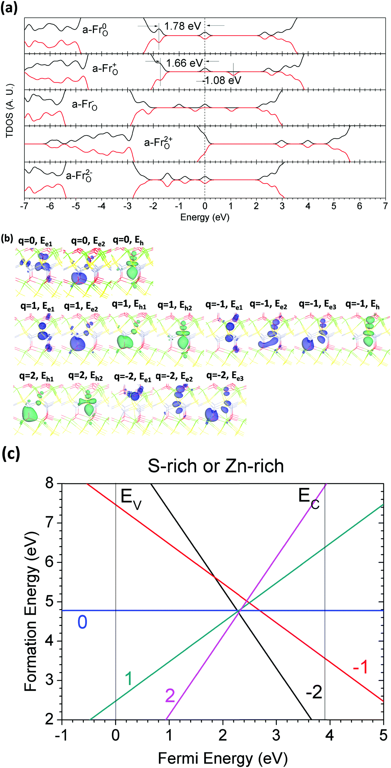 | ||
| Fig. 13 (a) TDOSs of a-Fr(O) in charge states of 0, +1, −1, +2, and −2. The dashed line denotes the highest occupied level for electrons. (b) Localized electron and hole orbitals at the relaxed a-Fr(O) site (Zn = gray, O = red, S = yellow, Ca = green). (c) Formation energies of a-Fr(O) under S- and Zn-rich chemical potential limits. | ||
 | ||
| Fig. 14 (a) TDOSs of VCaZnOS in charge states of 0, +1, −1, +2, and −2. The dashed line denotes the highest occupied level for electrons. (b) Localized electron and hole orbitals at the relaxed VCaZnOS site (Zn = gray, O = red, S = yellow, Ca = green). (c) Formation energies of VCaZnOS under S- and Zn-rich chemical potential limits. | ||
Native defect-induced luminescence properties
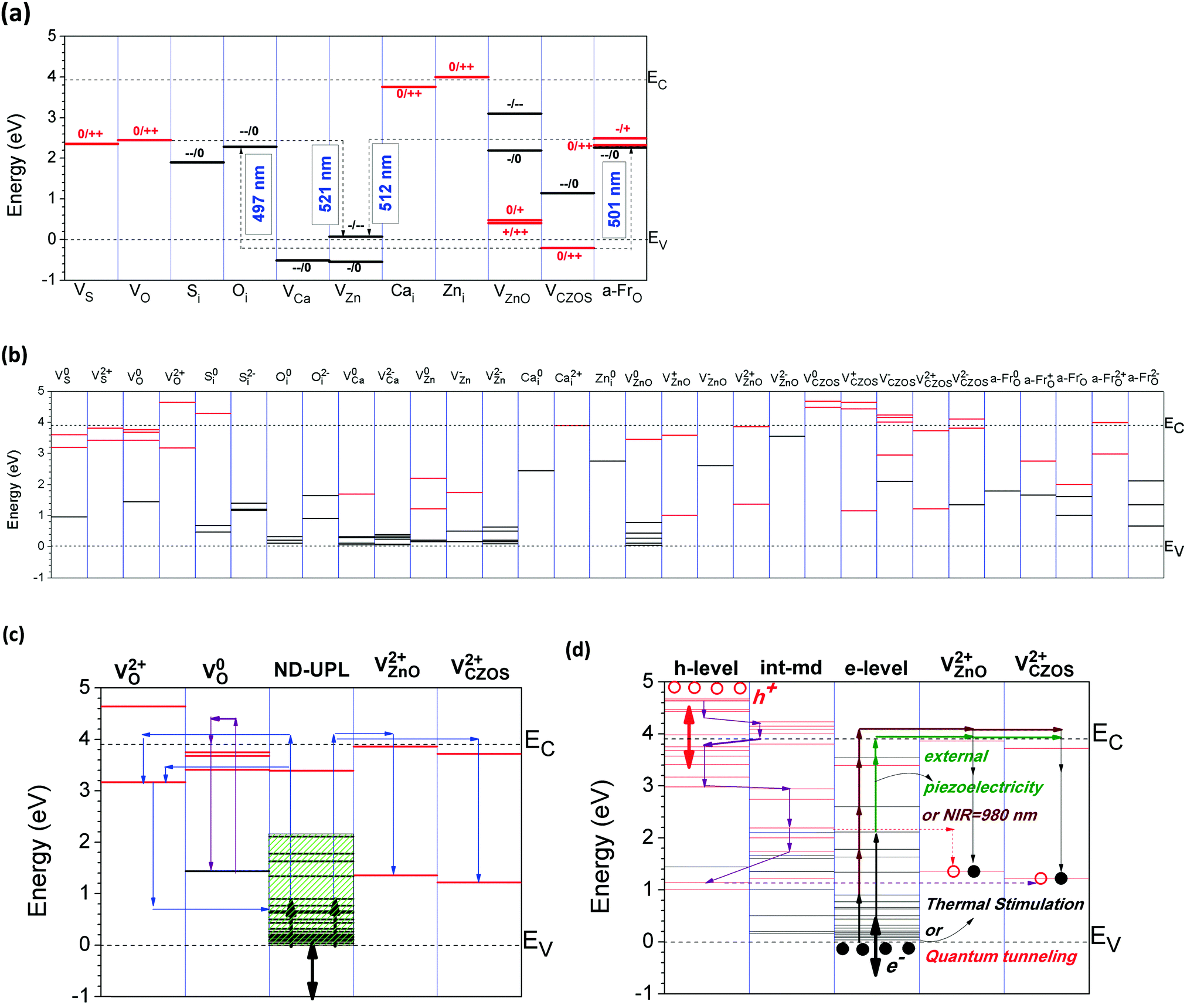 | ||
| Fig. 15 (a) Summary of thermodynamic transition levels of different charge states of the intrinsic defects of CaZnOS. The red lines denote donor-type transition levels and the black lines show the acceptor levels. (b) Summarized single-particle levels of intrinsic defects in CaZnOS with different charge states (empty states = red, filled states = black). (c) Native defects (N. D.) and dopant levels related to the upconverted persistent luminescence (UPL) mechanism. The black arrow denotes the electronic excitation directions through thermal stimulation or quantum tunneling effects. The green shaded area converse the lengthened optical transition path for persistent luminescence, which is an intact “supply line” for electron transport. The blue folded line shows the three different electronic transport paths for upconverted persistent luminescence. The violet folded line shows the O-related F-center fluorescence. (d) The transport mechanism of charge carriers and energy conversions for upconverted mechano-persistent luminescence. | ||
The experimentally observed broadened persistent luminescence peak is due to many possible native point defect levels, which participate in or assist the processes of optical excitation and emission. However, the essential point for persistent luminescence is the energy release at the activator/sensitizer site in the form of photon radiations, whose energies are originally transported from the storage sites of the excited energy. Actually, when native point defects are studied, this excited energy storage can be seen to arise from the trapping and transporting of excited electrons between different localized defect levels within the fundamental optical band gap. In previous work, we illustrated the energy conversion mechanism of intrinsic upconverted persistent luminescence in Er2O3.34 Here, we use this model to illustrate the descent mechanism of the intrinsic phosphorescence of CaZnOS, with the assistance of the calculation results of the single-particle levels and thermodynamic transition levels (ionization energy).
Here, we elucidate the intrinsic persistent luminescence mechanism of CaZnOS. From Table 3 and Fig. 15(a), we find that the VO and VZnO account for the lowest and the second lowest energy defects under the Zn-rich chemical potential limit, while Oi is the lowest energy defect under the S-rich limit. According to the related single particle levels, we found that only V2+O, V2+ZnO, and VCaZnOS correspond to the native activators which enable the localized levels to accommodate the transported charge carriers. The resulting recombination of charge carriers between the localized levels will release corresponding photon energies that are close to the experimental data, which is 2.48 eV (500 nm). The transport of charge carriers is accomplished by the localized electrons and hole levels near the VBM and CBM, respectively.
| S-rich | Zn-rich | S-rich | Zn-rich | ||||
|---|---|---|---|---|---|---|---|
| VS | 0 | 5.01 | 2.01 | VCa | 0 | 3.88 | 7.22 |
| +1 | 3.07 | 0.07 | −1 | 3.39 | 6.74 | ||
| +2 | 0.29 | −2.71 | −2 | 2.85 | 6.20 | ||
| VO | 0 | 4.95 | 0.23 | VZn | 0 | 3.41 | 5.38 |
| +1 | 2.60 | −2.12 | −1 | 2.86 | 4.83 | ||
| +2 | 0.05 | −4.67 | −2 | 2.93 | 4.90 | ||
| Si | 0 | 1.73 | 4.73 | Cai | 0 | 8.72 | 5.37 |
| −1 | 4.60 | 7.59 | +1 | 5.80 | 2.45 | ||
| −2 | 5.52 | 8.48 | +2 | 1.20 | −2.15 | ||
| Oi | 0 | 0.02 | 4.74 | Zni | 0 | 6.01 | 4.04 |
| −1 | 2.74 | 7.46 | +1 | 2.26 | 0.28 | ||
| −2 | 4.60 | 9.32 | +2 | −1.98 | −3.96 | ||
| VZnO | −2 | 4.44 | 3.07 | a-Fr(O) | −2 | 4.66 | 4.66 |
| −1 | 2.89 | 1.52 | −1 | 3.73 | 3.73 | ||
| 0 | 1.79 | 0.42 | 0 | 2.39 | 2.39 | ||
| +1 | 1.55 | 0.18 | +1 | 1.24 | 1.24 | ||
| +2 | 1.35 | −0.02 | +2 | 0.06 | 0.06 | ||
| VCaZnOS | −2 | 1.64 | 1.64 | a-Fr(S) | 0 | 3.28 | 3.28 |
| −1 | 1.46 | 1.46 | VCaS | 0 | 2.67 | 2.84 | |
| 0 | 1.07 | 1.07 | VCaO | 0 | 2.13 | 1.44 | |
| +1 | 1.13 | 1.13 | VZnS | 0 | 2.31 | 1.79 | |
| +2 | 1.17 | 1.17 | |||||
There are four possible luminescence mechanisms with different energy conversion and electron transport paths, as shown in Fig. 15(c): one is oxygen vacancy (VO) related F-center fluorescence, and the other three involve upconverted phosphorescence with different activator sites and electron transport paths. As we know, in luminescent materials, VO is usually a color center (or F-center).34,39 In CaZnOS, VO can be formed with very low formation energy under the Zn-rich chemical limit. This F-center dominant fluorescence by VO with −Ueff means that the emission is a two-electron process. The experimental reported UV photo-irradiation excitation wavelength of 378 nm (3.28 eV) provides high enough photon energies to activate the electrons that are trapped at the VO site to be excited into the CB or the state near the CB edge. The electrons will be de-excited back to the original ground states, with four possible emissions with energies of 2.03 eV (611 nm), 2.24 eV (554 nm), 2.31 eV (537 nm), and 2.46 eV (504 nm), which originate from three localized hole states and the CB edge, respectively. The experimentally reported intrinsic persistent luminescence from the host lattice is a wide green emission centered at 2.48 eV (500 nm). We can see that the photon emission from the CB edge to the localized electronic level has relatively high potential, as the external excitation energy is sufficiently high to pump electrons into the CB (3.28 eV). Thus, the emission spectrum we found is confirmed to have partial contributions of F-center excitations and emissions to the fluorescence at the V0O site, which is shown as a violet folded line in Fig. 15(c).
However, the F-center dominated fluorescence by the electronic transitions at the VO site usually possesses a time duration of luminescence in the magnitude of 10−9 s (∼ns), which means the intrinsic persistent luminescence does not essentially rely on this energy conversion and charge carrier transport. Therefore, it is unlikely that the VO alone contributes to the intrinsic persistent luminescence. The thermodynamic transition level of the VO site also supports this, as shown in Fig. 15(b), since the electronic transition along the zero-phonon-line between the CB edge and (0/2+) of VO does not match the required photon energy from the experimental emission spectrum.48 Therefore, although the ladder-like fine levels given by the native point defect states provide storage levels for electronic upconversion transport, the energy still decays quickly by depletion of energy mismatch.
Two other mechanisms we proposed are based on an energy conversion model related to different defect reactions within different charge states.34 The electrons in the excitation and de-excitation are transported along the zero-phonon line (ZPL), where the released energy contributes the photon energies with the largest quantum yields. In Fig. 14(c), the blue and pink folded lines denote the possible paths for electron excitation and de-excitation corresponding to the absorption and emission of the optical spectrum, in agreement with the experimental photon energy of 2.48 eV.
The formation energy calculations within different charge states are summarized in Table 3. In the neutral state under the S-rich limit, Oi is the lowest energy defect, with nearly zero formation energy, which denotes an almost spontaneous process. Meanwhile, under the Zn-rich limit, V0O has the lowest formation energy in the neutral state and VZnO has the second lowest formation energy. From Fig. 15(a) and (c), we can also confirm that V2+O, V2+ZnO, and V2+CaZnOS can all function as activator sites; in luminescence, the key requirement is deep electron trap levels as a storage center, where electrons can be continuously transported to the excited states and release photons by recombination with the holes at the activator sites or energy transfer from a higher excitation state to the lower ground state levels. Especially for V2+O, the localized hole states will accommodate the excited electrons going through and transferring back to the ground state electronic levels near the VBM, which remain near each other. The energy released in the form of photon energy indeed has a relatively wide range, as shown in Fig. 15(c), which agrees with the experimentally reported broad green emission peak.48
These three upconverted phosphorescence processes arise because with the formation of native point defects, the fine electronic levels are localized near the VBM. The electrons from the VBM easily interact with the localized defect levels of Oi and VZn, as their electronic levels remain near the top of the VB. The electrons will be transported to the higher levels gradually through upconverted energy conversions, with an energy scale of thermal stimulation (0.1 to 0.2 eV) or quantum tunneling effects. The electrons will finally be excited to the delocalized states in the CB by 378 nm UV photo-irradiation and release photons (2.50 eV) in the emission transfer from the higher localized state to lower levels at the V2+ZnO site. Meanwhile, the electrons will continuously fill the occupied localized levels of VO through thermal stimulation or tunneling effects with ladder-like levels localized near the VBM contributed by the native point defects, such as Oi and VZn, within different charge states. These electrons are available as storage levels to supply enough charge carriers to be excited for long-lasting energy conversions during persistent luminescence.
From the single particle levels in Fig. 15(a), we can see that the electrons can be easily excited by thermal perturbation from the VBM to the localized levels produced by the Zn-vacancy (VZn). We have already shown the native point defects in terms of the various charge states. We can see that the charge transition level of (0/2+) of VO is located at EV + 2.45 eV, where the VBM is EV = 0. We have found that in lattice presentations similar to the ZnO wurtzite lattice, Schottky pair defects have lower formation energies than Frenkel pair defects (both cation and anion types). We also found that the reported phosphor in ZnO may be provided by the energy transfer between VO and VZn from (0/2+) to (2−/0), respectively, in a two-photon process. Similar observations have been made by Stehr et al.82 The vacancies of Ca and Zn in the CaZnOS lattice are acceptor (hole trap) centers that capture electrons. We can see that the transition level (2−/−) of Zn is at EV + 0.07 eV, which means that it almost remains at the VBM. This will provide a large amount of freely conductive or delocalized holes at the VB as activators.
Fig. 15(d) shows the mechanism for the energy conversion of the intrinsic upconverted mechano-persistent luminescence in CaZnOS. We see that various type of native point defects within different charge states contribute different roles to transport the bounded charges to the positions for recombination, as summarized in Table 4. The e-levels shown in Table 4 and Fig. 15(d) act as extra deep donors localized near the VBM, while the h-levels are extra deep holes next to the CBM. The int-mid levels are native point defect levels acting as intermediates to combine the holes from the CBM and the electrons from the VBM to a deeper range in the band gap. The charges will then move uphill through a very small energy barrier, aided by thermostimulation or a quantum tunneling effect, to reach deeper levels within the band gap area. With further external excitations, such as mechano-stimuli, friction, piezoelectric fields, NIR, or UV light, the charges will further alternate with each other, as shown in Fig. 15(d). The recombination of these opposite charges will release the energy as photons.
| h-level | O0i | O2−i | V2−Zn | V0ZnO | V−ZnO | V2−ZnO | a-Fr0O | a-Fr2−O |
| int-mid | V0O | V2+O | V+ZnO | V0CaZnOS | V+CaZnOS | a-Fr2+O | ||
| e-level | V0Zn | V−Zn | V−CaZnOS | V2−CaZnOS | a-Fr+O | a-Fr−O |
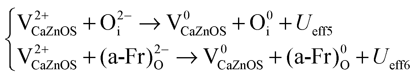
However, we believe it is still not very clear how the energy conversion and electrons are transported during the process of persistent luminescence, and how the energy is converted in the three different luminescence mechanisms. We proposed the ECCR (energy converted chain reaction) model in a previous study on intrinsic upconverted persistent luminescence in Er2O3.34 This model bridges the relationship between single particle levels and thermodynamic transition levels, and it projects the essential electron transitions along the zero-phonon line, which matches the experimental emissions and upconverted conversions, through a series of defect reactions. Therefore, based on Fig. 15(c), we here consider the related native point defect reactions within different charge states under external excitation. The persistent luminescence occurs in the energy transfer by the transport of charge carriers between the deep levels near the mid-gap, as demonstrated with the following defect reactions in the form of a two-electron process for each defect reaction along the zero-phonon line:
 | (5) |
 | (6) |
 | (7) |
 | (8) |
From eqn (5), a V0O state will release two electrons from the site which will be captured by two V0Zn, as VZn is a shallow acceptor site; each V0Zn captures the electrons and transforms into V−Zn, with an even lower energy (Table 3 and Fig. 15(b)). The reaction of V0Zn to V−Zn releases a hole at the same time. The remaining V0O will further continue the electron transfer with the two V−Zn, with further reaction of V−Zn to V2−Zn when V0O transforms to V2+O. This will release the as-discussed Ueff1 and Ueff2 from the above reactions.
Moreover, we know the Ueff from these reactions are released/absorbed energy with effective correlation energy in form of the energy cost of electrons pairing at the same point defect sites. This is necessary to consider within the framework of chemical thermodynamics. Firstly, the system (the CaZnOS host lattice) contains different types of native point defects. We modeled these under ideal conditions where all of the defects are perfectly solved in the solvent where the host lattice is located and are freely dynamically mobile under thermal stimulation or external UV excitation. Accordingly, these native point defects mutually react with each other to convert the energy as well as transport the excited electrons.
The experimentally reported intrinsic phosphorescence of CaZnOS is centered at about 500 nm, with a broad peak from 480 nm to 520 nm. The related photon energies are in the range from 2.38 eV to 2.58 eV. We learned that this wide wavelength range of phosphorescence is attributed to electrons continuously recombining with holes at a level near the VB edge. Without applying any external stress, the (2−/−) of VZn is at the VBM; when there is UV photo-irradiation or an external stress-induced piezoelectric field forms, local charge separation occurs. The defects will undergo a series of charge chemical reactions, with associated energy conversion. As we know, VZn is the site that captures electrons with released holes as an acceptor trap according to the reaction V0Zn → V−Zn + h → V2−Zn + 2h, where h denotes the holes. In contrast to the acceptor trap site, the VO acts as a deep donor trap site and has a defect reaction of V0O → V2+O + 2e. The two electrons released from the original V+O sites will automatically transform themselves to V0O and V2+O respectively due to negative-Ueff, with a reaction of 2V+O → V0O + V2+O. Therefore, the electrons at VO are doubly occupied or empty, and the related emissions given by this charge carrier recombination are usually two-photon processes.
From the defect reactions shown in eqn (5), (6) and (8), the effective correlation energies for these two-electron related defect reactions are Ueff1 = −6.00 eV, Ueff2 = −4.76 eV, Ueff3 = +1.22 eV, Ueff4 = +9.54 eV, Ueff5 = −4.98 eV, and Ueff6 = −4.94 eV, respectively. This shows the coexistence of exothermal and endothermal reactions. The negative effective correlation energies show that the two electrons will overcome the repulsive Coulomb potential to correlate with each other as a pair to be doubly occupied at the defect site, such as V2−CaZnOS, O2−i, or a-Fr2−O. Then, the energies released or absorbed per electron from each defect reaction above are 3.00 eV, 2.38 eV, 0.61 eV, 4.77 eV, 2.49 eV, and 2.47 eV, respectively. The experimental reported intrinsic wide green luminescence has a peak centered at 500 nm (2.48 eV). If our predicted energies can be released in wavelength in terms of photons, the value with 521 nm (2.37 eV) has a mean relative error (MRE) of 4%. Considering that the acceptable error usually found in experimental measurements is 30% to 50%,83 this prediction is confirmed from our energy conversion model with good consistency and in agreement with experimental observations.48Eqn (5), (6) and (8) actually show a defect reaction cycle. In ideal cases, the reactions with Ueff1 and Ueff2 will combine and are found to be exactly the same as the energy barrier given by the reaction with Ueff3 and Ueff4. Therefore, the native point defects will repeatedly participate in the reaction cycle with specific quantum yield (reaction efficiency) in a practical scenario. The intrinsic persistent luminescence will continue until all of the energies released from eqn (5), (6) and (8) decay to zero.
The defect reactions shown above in eqn (7) support the possible energy conversion of electrons transported from the VB to the higher excited states near the CB or in the CB. These electrons originally initiated from either the Oi site, the VCaZnOS site, or the a-Fr(O) site, which are the source centers supplying electrons. On the other hand, they can very readily form in the host lattice due to the relatively low formation energy per defect site (shown in Table 3). As we can see from the Oi site, O0i provides the localized electronic states near the VBM. As discussed in previous sections, these are actually fine levels which facilitate the migration of electrons from the VBM through thermal stimulations and quantum tunneling effects. Under external UV excitation (378 nm), the charges (including electrons and holes) are separately excited to states near the CB and VB, respectively, so as to ionize the native point defect sites. Consequently, V2+O, V2+ZnO, and V2+CaZnOS are activator sites that accommodate recombination of these charge carriers. Further supported by our single particle level calculations, we found that the electronic states of VZnO near the VBM can also participate in this process by coupling with different defect levels to accomplish charge transformation through the native point defect site.
We can see that the transition level of VO is at EV + 2.45 eV and the VZn transition level is at about EV + 0.07 eV, while EV = 0 for VBM. Therefore, it is continuously extracting electrons from the valence band or exchanging electrons/holes at the VBM. The recombination path is between the transition level of VO and the VBM. With external UV excitations of 378 nm, the electrons at the VBM are excited to higher occupied states localized near the CB or far away from the VBM, while the holes from the CB are also excited to the localized empty states near the VBM. Therefore, the process of charge separation and rearrangement is based on the native point defect levels in the host lattice. Therefore, for the activator site V2+ZnO, the lower localized hole state can accommodate the holes excited from the CB.
| A(t) = (1 − η)tA0 | (9) |
In most phosphor materials, if η is a very small constant (0 < η ≪ 1), eqn (9) can be approximately simplified into the first order chemical reaction rate equation, as follows:
 | (10) |
Ideally, the number of photons generated is in proportion to the concentration of a-Fr defects at each time moment. Then, regardless of the approximation of eqn (10), the number of photons generated by CCR at the t-th cycle is shown exactly as:
| Nphoton(t) = (η)tNphoton(0) | (11) |
If we simply assume the emission intensity is proportional to the number of photons, this allows IPL(t) ∝ Nphoton(t). Thus, the persistent luminescence decay spectrum can be simulated as the given equation based on eqn (11):
IPL(t) = (η)tIPL(0) and t1/2 = −(ln![[thin space (1/6-em)]](https://www.rsc.org/images/entities/char_2009.gif) 2/lnη) 2/lnη) | (12) |
(a) Independent energy conversion model. For the experimentally reported wide green emission peak, we can model this as three persistent luminescence mechanisms with three independent energy conversion models with a simple linear combination. Fig. 16(a) is an example for eqn (5) and (6), while eqn (8) can also follow the scheme shown in Fig. 15(a). This means that if we consider eqn (8) as relatively independent of the chain reactions of eqn (1) and (2), the rate of reaction at a moment t is provided:
| A(t) = A1(t) + A2(t) + A3(t) = (1 − η1)tA10 + (1 − η2)tA20 + (1 − η3)tA30 | (13) |
 | (14) |
A(t) is actually the total concentration of the VZnO, VCaZnOS, and a-FrO defects related to the time after the external photo-excitations; A10, A20, and A30 are their initial concentrations, respectively. We can see that eqn (14) is the linear combination of three different first-order chemical reactions, which is similar to the radiation decay phenomenon.
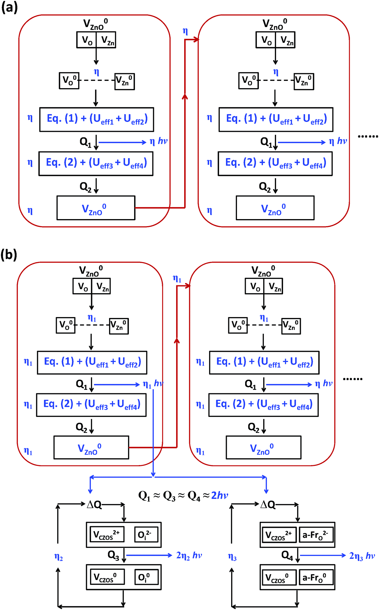 | ||
| Fig. 16 (a and b) Detailed schematics of the process of energy conversion within a group of native point defects between different charge states. | ||
We find the behavior of eqn (14) is very similar to the experiments of persistent luminescence.20,21,37,83Eqn (9) and (10) show the cases of single luminescence peaks within different charge states due to the subtle interplay of multi-defect reactions. For a single persistent luminescence peak with −Ueff for O-defects, eqn (11) seems to be valid in many cases. Considering eqn (5a), the intensity of three independent chain reactions is shown as follows:
| IPL(t) = (2η1)tIPL1(0) + (2η2)tIPL2(0) + (2η3)tIPL3(0) | (15) |
2/ln2(η1 + η2 + η3)] if the approximation (2η1)t + (2η2)t + (2η3)t ≈ 2t(η1 + η2 + η3)t is valid for small η.
(b) Serial-type energy conversions. Considering Fig. 15(c), it seems the energy conversion of eqn (8) is originally sourced from eqn (5) and (6) with further efficiencies of η2 and η3. We accordingly further modify the chain reactions with consideration of the ECCR model, as shown in Fig. 16(b). Therefore, eqn (9) is re-directed to become a new equation if the chain reactions from eqn (5)–(8) are a serial type of ECCR model whose driving energies are originally sourced from the defect reactions of eqn (5); the rate equation is updated as follows:
| A(t) = A1(t) + A2(t) + A3(t) = (1 − η1)tA10 + [η1(1 − η2)]tA20 + [η1(1 − η3)]tA30 | (16) |
| IPL(t) = (2η1)tIPL1(0) + (2η1η2)tIPL2(0) + (2η1η3)tIPL3(0) | (17) |
From eqn (15) and (17), the so-called half-life of persistent luminescence is a parameter that reflects the intrinsic properties of the as-synthesized phosphor materials. With consideration of both cases above (independent and serial type), enlarging the η is actually the core factor that prolongs the duration time of the persistent luminescence. However, it is wise to increase the defect concentration and reduce the defect reaction activation barrier. Usually, this involves increasing the defect concentration of materials in a packed structure.84–87
Role of defect determination and comparison
We also considered a lattice with various defects with low formation energies and compared this with experimental synthesized samples using X-ray diffraction patterns. Although the comparison is qualitative, the physical and chemical trends for the influence of defects will be consistent with experimental synthesized results and potentially be a reference for future modulations of properties.Fig. 17(a) shows the theoretical X-ray diffraction (XRD) pattern of the ideal CaZnOS lattice. It shows an evident match with the experimental measured XRD from Pan et al.6 and Lian et al.48
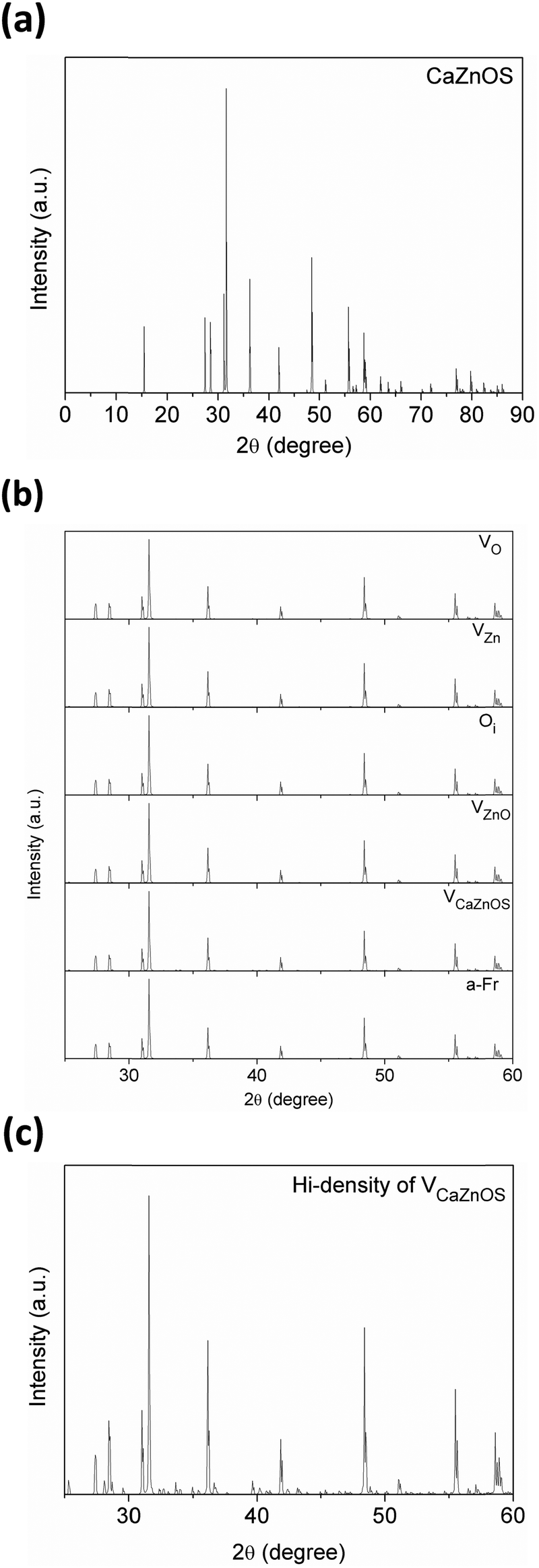 | ||
| Fig. 17 (a) Theoretical XRD pattern of the ideal CaZnOS lattice. (b) Theoretical XRD patterns of CaZnOS with VO, VZn, Oi, VZnO, VCaZnOS, and a-FrO in relatively low amounts. (c) Theoretical XRD pattern of CaZnOS with a high density of VCaZnOS. | ||
To consider this further, we included the low formation energy defects such as VO, VZn, Oi, VZnO, VCaZnOS, and a-FrO in CaZnOS for the XRD simulation. As shown in Fig. 17(b), the XRD peaks at about 27° show a trend of broadening similar to the work of Lian et al.48 As we know, the experiments by Lian et al. were performed in an atmosphere of N2 flow for both single phase CaZnOS and doped CaZnOS.48 They further showed that the twin peaks at 27° merge to a single peak under H2/N2 flow, denoting that H will passivate the defect sites, in accordance with our defect analysis. The twin peaks at 32° become wider in defective CaZnOS in our simulated XRD, in a similar trend to that of Pan et al.6 The powder samples synthesized by Pan et al. experienced sintering under Ar atmosphere and were ground again after cooling of the sintered powder. These different treatments of the CaZnOS samples may be the cause of the slight differences in the XRD spectra of Pan et al.6 and Lian et al.48
To approach a more realistic situation, we increased the amount of VCaZnOS (Schottky type defect) in the same size CaZnOS supercell. Fig. 17(c) shows that the newly induced satellite peaks at 27° and 32° are more obvious and are in good agreement with the sample synthesized by Pan et al.6 Thus, experimentally grinding the sintered sample after cooling it will vastly increase the amount of VCaZnOS or form other, similar vacancy defects.
Conclusion
We have studied the native point defect levels of CaZnOS to interpret its intrinsic persistent luminescence mechanism. We found that low energy vacancy-type defects, such as Zn and O vacancies, and Schottky defects mutually interplay through a series of defect chemical reactions to transport charges and convert the energies within different lattice sites and charge states. Under the S-rich limit, interstitial O has a very low formation energy and readily captures paired electrons to release holes. The CaZnOS stoichiometric vacancy (Schottky type) is the second lowest energy defect, with 1.07 eV per defect site, and the ZnO vacancy is the third lowest. Under the Zn-rich chemical potential limit, the O vacancy is the lowest energy defect with 0.23 eV, and the ZnO vacancy is the second lowest with an energy of 0.42 eV, similar in magnitude to the O vacancy. The Zn vacancy is an active hole center with a +Ueff because it releases about 0.55 eV to free a hole by capturing a localized electron near the anion (S, O) sites. In defect reaction-related energy conversion, the ZnO and CaZnOS vacancies are the native activator sites to accommodate the recombination of the excited electrons and holes and release the energy by photon emission.Acknowledgements
The author gratefully acknowledges the support of the Natural Science Foundation of China (NSFC) for the Youth Scientist grant (Grant No. NSFC 11504309), the initial start-up grant support from the Department General Research Fund (Dept. GRF) from ABCT in the Hong Kong Polytechnic University, and the Early Career Scheme (ECS) fund (Grant No. PolyU 253026/16P) from the Research Grant Council (RGC) in Hong Kong.References
- Z. L. Wang, Nano Today, 2010, 5, 540 CrossRef CAS.
- W. Wu and Z. L. Wang, Nature Reviews Materials, 2016, 16031 CrossRef.
- X. Wang, et al. , Adv. Mater., 2015, 27, 2324 CrossRef CAS PubMed.
- D. Peng, B. Chen and F. Wang, ChemPlusChem, 2015, 80, 1209 CrossRef CAS.
- D. Tu, C.-N. Xu, Y. Fujio and A. Yoshida, Light: Sci. Appl., 2015, 4, e356 CrossRef CAS.
- H. Zhang, D. Peng, W. Wang, L. Dong and C. Pan, J. Phys. Chem. C, 2015, 119, 28136 CAS.
- Y. Zhang, G. Gao, H. L. W. Chan, J. Dai, Y. Wang and J. Hao, Adv. Mater., 2012, 24, 1729 CrossRef CAS PubMed.
- M.-C. Wong, L. Chen, M.-K. Tsang, Y. Zhang and J. Hao, Adv. Mater., 2015, 27, 4488 CrossRef CAS PubMed.
- L.-B. Huang, G. Bai, M.-C. Wong, Z. Yang, W. Xu and J. Hao, Adv. Mater., 2016, 28, 2744 CrossRef CAS PubMed.
- J.-C. Zhang, C.-N. Xu, S. Kamimura, Y. Terasawa, H. Yamada and X. Wang, Opt. Express, 2013, 21, 12976 CrossRef CAS PubMed.
- J.-C. Zhang, L.-Z. Zhao, Y.-Z. Long, H.-D. Zhang, B. Sun, W.-P. Han, X. Yan and X. Wang, Chem. Mater., 2015, 27, 7481 CrossRef CAS.
- T. Aitasalo, P. Dereń, J. Hölsä, H. Jungner, J. C. Krupa, M. Lastusaari, J. Legendziewicz, J. Niittykoski and W. Stręk, J. Solid State Chem., 2003, 171, 114 CrossRef CAS.
- T. Matsuzawa, Y. Aoki, N. Takeuchi and Y. Murayama, J. Electrochem. Soc., 1996, 143, 2670 CrossRef CAS.
- K. Van den Eeckhout, P. F. Smet and D. Poelman, Materials, 2010, 3, 2536 CrossRef CAS.
- K. Van den Eeckhout, D. Poelman and P. Smet, Materials, 2013, 6, 2789 CrossRef CAS.
- Z. Pan, Y.-Y. Lu and F. Liu, Nat. Mater., 2012, 11, 58 CrossRef CAS PubMed.
- T. Maldiney, et al. , Nat. Mater., 2014, 13, 418 CrossRef CAS PubMed.
- A. Abdukayum, J.-T. Chen, Q. Zhao and X.-P. Yan, J. Am. Chem. Soc., 2013, 135, 14125 CrossRef CAS PubMed.
- Z. Li, Y. Zhang, X. Wu, L. Huang, D. Li, W. Fan and G. Han, J. Am. Chem. Soc., 2015, 137, 5304 CrossRef CAS PubMed.
- D. C. Rodriguez Burbano, E. M. Rodriguez, P. Dorenbos, M. Bettinelli and J. A. Capobianco, J. Mater. Chem. C, 2014, 2, 228 RSC.
- D. C. Rodríguez Burbano, S. K. Sharma, P. Dorenbos, B. Viana and J. A. Capobianco, Adv. Opt. Mater., 2015, 3, 551 CrossRef.
- G.-Y. Adachi and N. Imanaka, Chem. Rev., 1998, 98, 1479 CrossRef CAS.
- P. F. Smet, I. Moreels, Z. Hens and D. Poelman, Materials, 2010, 3, 2834 CrossRef CAS.
- J. Hölsä, Electrochem. Soc. Interface, 2009, 18, 42 Search PubMed.
- F. Auzel, Chem. Rev., 2004, 104, 139 CrossRef CAS PubMed.
- L.-D. Sun, Y.-F. Wang and C.-H. Yan, Acc. Chem. Res., 2014, 47, 1001 CrossRef CAS PubMed.
- X. Liu, C.-H. Yan and J. A. Capobianco, Chem. Soc. Rev., 2015, 44, 1299 RSC.
- L.-D. Sun, H. Dong, P.-Z. Zhang and C.-H. Yan, Annu. Rev. Phys. Chem., 2015, 66, 619 CrossRef CAS PubMed.
- H. Dong, L.-D. Sun and C.-H. Yan, Chem. Soc. Rev., 2015, 44, 1608 RSC.
- Z.-J. Zhang, A. Feng, X.-Y. Chen and J.-T. Zhao, J. Appl. Phys., 2013, 114, 213518 CrossRef.
- T.-W. Kuo, W.-R. Liu and T.-M. Chen, Opt. Express, 2010, 18, 8187 CrossRef CAS PubMed.
- P. Gluchowski, W. Strek, M. Lastusaari and J. Holsa, Phys. Chem. Chem. Phys., 2015, 17, 17246 RSC.
- B. Huang, Inorg. Chem., 2015, 54, 11423 CrossRef CAS PubMed.
- B. Huang, Phys. Chem. Chem. Phys., 2016, 18, 13564 RSC.
- B. Huang, R. Gillen and J. Robertson, J. Phys. Chem. C, 2014, 118, 24248 CAS.
- B. Huang, Philos. Mag., 2014, 94, 3052 CrossRef CAS.
- T. Maldiney, A. Lecointre, B. Viana, A. Bessière, M. Bessodes, D. Gourier, C. Richard and D. Scherman, J. Am. Chem. Soc., 2011, 133, 11810 CrossRef CAS PubMed.
- A. De Vos, K. Lejaeghere, D. E. P. Vanpoucke, J. J. Joos, P. F. Smet and K. Hemelsoet, Inorg. Chem., 2016, 55, 2402 CrossRef CAS PubMed.
- B. Qu, B. Zhang, L. Wang, R. Zhou and X. C. Zeng, Chem. Mater., 2015, 27, 2195 CrossRef CAS.
- K. Huang and A. Rhys, Proc. R. Soc. London, Ser. A, 1950, 204, 406 CrossRef CAS.
- B. Huang and J. Robertson, Phys. Rev. B: Condens. Matter Mater. Phys., 2012, 85, 125305 CrossRef.
- B. Huang and J. Robertson, J. Non-Cryst. Solids, 2012, 358, 2393 CrossRef CAS.
- B. Huang, Phys. Status Solidi B, 2015, 252, 431 CrossRef CAS.
- I. Dursun, C. Shen, M. R. Parida, J. Pan, S. P. Sarmah, D. Priante, N. Alyami, J. Liu, M. I. Saidaminov, M. S. Alias, A. L. Abdelhady, T. K. Ng, O. F. Mohammed, B. S. Ooi and O. M. Bakr, ACS Photonics, 2016, 3, 1150–1156 CrossRef CAS.
- M. Peplow, C&EN News, 22nd June 2016.
- H. C. Hsu, C. I. Lin and H. K. Chen, Metall. Mater. Trans. B, 2004, 35, 55–63 CrossRef.
- T. Sambrook, C. F. Smura, S. J. Clarke, K. M. Ok and P. S. Halasyamani, Inorg. Chem., 2007, 46, 2571 CrossRef CAS PubMed.
- Z. Qiu, C. Rong, W. Zhou, J. Zhang, C. Li, L. Yu, S. Liu and S. Lian, J. Alloys Compd., 2014, 583, 335 CrossRef CAS.
- Y. Ding, J. Gu, J. Ke, Y.-W. Zhang and C.-H. Yan, Angew. Chem., Int. Ed., 2011, 50, 12330 CrossRef CAS PubMed.
- S. J. Clark, M. D. Segall, C. J. Pickard, P. J. Hasnip, M. I. J. Probert, K. Refson and M. C. Payne, Z. Kristallogr., 2005, 220, 567 CAS.
- C. J. Pickard, B. Winkler, R. K. Chen, M. C. Payne, M. H. Lee, J. S. Lin, J. A. White, V. Milman and D. Vanderbilt, Phys. Rev. Lett., 2000, 85, 5122 CrossRef CAS PubMed.
- B. Huang, Solid State Commun., 2016, 230, 49 CrossRef CAS.
- B. Huang, Solid State Commun., 2016, 237–238, 34 CrossRef CAS.
- I. A. Vladimir, F. Aryasetiawan and A. I. Lichtenstein, J. Phys.: Condens. Matter, 1997, 9, 767 CrossRef.
- S. Lany and A. Zunger, Phys. Rev. B: Condens. Matter Mater. Phys., 2009, 80, 085202 CrossRef.
- S. Lany and A. Zunger, Phys. Rev. B: Condens. Matter Mater. Phys., 2010, 81, 205209 CrossRef.
- B. J. Morgan and G. W. Watson, J. Phys. Chem. C, 2010, 114, 2321 CAS.
- P. R. L. Keating, D. O. Scanlon, B. J. Morgan, N. M. Galea and G. W. Watson, J. Phys. Chem. C, 2011, 116, 2443 Search PubMed.
- B. Huang, J. Comput. Chem., 2016, 37, 825 CrossRef CAS PubMed.
- T. Zacherle, A. Schriever, R. A. De Souza and M. Martin, Phys. Rev. B: Condens. Matter Mater. Phys., 2013, 87, 134104 CrossRef.
- L. Kleinman and D. M. Bylander, Phys. Rev. Lett., 1982, 48, 1425 CrossRef CAS.
- S. G. Louie, S. Froyen and M. L. Cohen, Phys. Rev. B: Condens. Matter Mater. Phys., 1982, 26, 1738 CrossRef CAS.
- A. M. Rappe, K. M. Rabe, E. Kaxiras and J. D. Joannopoulos, Phys. Rev. B: Condens. Matter Mater. Phys., 1990, 41, 1227 CrossRef.
- P. J. Hasnip and C. J. Pickard, Comput. Phys. Commun., 2006, 174, 24 CrossRef CAS.
- K. Laasonen, A. Pasquarello, R. Car, C. Lee and D. Vanderbilt, Phys. Rev. B: Condens. Matter Mater. Phys., 1993, 47, 10142 CrossRef CAS.
- N. Marzari, D. Vanderbilt and M. C. Payne, Phys. Rev. Lett., 1997, 79, 1337 CrossRef CAS.
- M. I. J. Probert and M. C. Payne, Phys. Rev. B: Condens. Matter Mater. Phys., 2003, 67, 075204 CrossRef.
- J. D. Denlinger, J. A. Clack, J. W. Allen, G. H. Gweon, D. M. Poirier, C. G. Olson, J. L. Sarrao, A. D. Bianchi and Z. Fisk, Phys. Rev. Lett., 2002, 89, 157601 CrossRef CAS PubMed.
- H. J. Tromp, P. van Gelderen, P. J. Kelly, G. Brocks and P. A. Bobbert, Phys. Rev. Lett., 2001, 87, 016401 CrossRef CAS PubMed.
- Z. Wu, D. J. Singh and R. E. Cohen, Phys. Rev. B: Condens. Matter Mater. Phys., 2004, 69, 193105 CrossRef.
- S.-P. Gao, J. Jiang, M. Cao, J. Zhu and J. Yuan, Phys. Rev. B: Condens. Matter Mater. Phys., 2004, 69, 214419 CrossRef.
- S. J. Clark and J. Robertson, Phys. Rev. B: Condens. Matter Mater. Phys., 2010, 82, 085208 CrossRef.
- S. Lany and A. Zunger, Phys. Rev. B: Condens. Matter Mater. Phys., 2008, 78, 235104 CrossRef.
- S. A. Petrova, V. P. Mar'evich, R. G. Zakharov, E. N. Selivanov, V. M. Chumarev and L. Y. Udoeva, Dokl. Chem., 2003, 393, 255 CrossRef CAS.
- Z. L. Wang and J. Song, Science, 2006, 312, 242 CrossRef CAS PubMed.
- W. Zhong Lin, J. Phys.: Condens. Matter, 2004, 16, R829 CrossRef.
- C. J. Duan, A. C. A. Delsing and H. T. Hintzen, Chem. Mater., 2009, 21, 1010 CrossRef CAS.
- B. Huang, H. Dong, K.-L. Wong, L.-D. Sun and C.-H. Yan, J. Phys. Chem. C, 2016, 120, 18858–18870 CAS.
- S. Broadley, Z. A. Gál, F. Corà, C. F. Smura and S. J. Clarke, Inorg. Chem., 2005, 44, 9092 CrossRef CAS PubMed.
- S. Lany and A. Zunger, Phys. Rev. Lett., 2004, 93, 156404 CrossRef PubMed.
- S. Lany and A. Zunger, Phys. Rev. B: Condens. Matter Mater. Phys., 2005, 72, 035215 CrossRef.
- J. E. Stehr, S. L. Chen, N. K. Reddy, C. W. Tu, W. M. Chen and I. A. Buyanova, Adv. Funct. Mater., 2014, 24, 3760 CrossRef CAS.
- J. Wang, J. H. Hao and P. A. Tanner, J. Lumin., 2015, 164, 116 CrossRef CAS.
- D. A. Pejaković, J. Lumin., 2010, 130, 1048 CrossRef.
- J. Zhang, Z. Zhang and T. Wang, Chem. Mater., 2004, 16, 768 CrossRef CAS.
- P. G. Baranov, N. G. Romanov, D. O. Tolmachev, C. de Mello Donegá, A. Meijerink, S. B. Orlinskii and J. Schmidt, JETP Lett., 2006, 84, 400 CrossRef CAS.
- A. S. Gurin, N. G. Romanov, D. O. Tolmachev and P. G. Baranov, Phys. Solid State, 2015, 57, 280 CrossRef CAS.
| This journal is © the Owner Societies 2016 |