Dominant factors limiting the optical gain in layered two-dimensional halide perovskite thin films†
Received
24th March 2016
, Accepted 28th April 2016
First published on 28th April 2016
Abstract
Semiconductors are ubiquitous gain media for coherent light sources. Solution-processed three-dimensional (3D) halide perovskites (e.g., CH3NH3PbI3) with their outstanding room temperature optical gain properties are the latest members of this family. Their two-dimensional (2D) layered perovskite counterparts with natural multiple quantum well structures exhibit strong light–matter interactions and intense excitonic luminescence. However, despite such promising traits, there have been no reports on room temperature optical gain in 2D layered perovskites. Herein, we reveal the challenges towards achieving amplified spontaneous emission (ASE) in the archetypal (C6H5C2H4NH3)2PbI4 (or PEPI) system. Temperature-dependent transient spectroscopy uncovers the dominant free exciton trapping and bound biexciton formation pathways that compete effectively with biexcitonic gain. Phenomenological rate equation modeling predicts a large biexciton ASE threshold of ∼1.4 mJ cm−2, which is beyond the damage threshold of these materials. Importantly, these findings would rationalize the difficulties in achieving optical gain in 2D perovskites and provide new insights and suggestions for overcoming these challenges.
Introduction
Organic–inorganic lead halide perovskites have emerged as technologically important semiconductors due to recent discoveries of their outstanding optoelectronic properties.1–4 They can be categorized based on their structural dimensionality, with 2D (A2BX4 formula) and 3D (ABX3 formula) perovskites being the most studied materials. While disproportionate attention has been given to 3D perovskites for photovoltaics, there has also been a recent surge of interest in their light emitting1,5–7 and optical gain properties.3,8–11 2D perovskites had dominated the limelight in the past decades due to their potential for applications in light emitting diodes.12–16 Nonetheless, reports of optical gain in solution-processed 2D perovskite thin films are few and far between: out of 28 perovskite optical gain reports available to date, there is only one early report by Kondo et al.17 that claimed 2D perovskite cavity lasing at 16 K (see Fig. S1, ESI†). Although this report showed evidence of narrow emission linewidth at higher pump intensity, the light-in–light-out data presented did not indicate a clear transition from spontaneous emission to stimulated emission. As Samuel et al. pointed out, the lasing phenomenon should satisfy four criteria,18 namely: (1) narrow emission linewidth, (2) clear threshold associated with emission intensity and linewidth, (3) tunable light emission with laser cavity and gain medium, and (4) beam-like output (see Fig. S2, ESI†). It is important to ensure that all these criteria are fulfilled to eliminate phenomena with similar signatures from luminescent micro-cavities and waveguiding effects that could be mistakenly assigned as lasing. As such, it is highly possible (in view of the limited data available from the manuscript) that the “lasing” reported by Kondo et al.17 could in fact be a case of a luminescent microcavity or waveguiding effect (or a combination of both). Although the possibility of attaining lasing from 2D perovskites cannot be totally ruled out, it is surprising that reports on optical gain from 2D perovskites are scarcely available. 2D perovskites (e.g., (C6H5C2H4NH3)2PbI4 (hereafter called PEPI)), which exhibit a strong excitonic green emission, could be potential gain materials for overcoming the “green gap” in semiconductor lasers.19 In particular, PEPI has been extensively investigated for light emission applications in the 1990s and early 2000.13,14,20 The naturally formed quantum well in 2D perovskites is also attractive for integration into electrically pumped gated green lasers.21 The excellent in-plane mobility experienced by charge carriers in the inorganic quantum well is also expected to be better than four-level conjugated organic semiconductor systems which exhibit ASE.22 Unfortunately, the limited reports on 2D perovskite lasing clearly unpin the challenges in achieving optical gain from these materials. Detailed photophysical insights into the relaxation processes of the photoexcited species, as well as the dominant factors limiting the optical gain, are therefore urgently required.
Herein, we present a detailed photophysical study on solution-processed PEPI thin films using temperature and pump-fluence dependent photoluminescence (PL) spectroscopy. Room temperature PL spectroscopy using high laser pump fluence (of the order of 100 μJ cm−2) revealed a dominating free excitonic emission peak (peak 1) with a notable absence of ASE. Low temperature PL revealed a more significant bound excitonic emission peak (peak 2) with a third biexcitonic emission peak (peak 3) appearing at higher laser excitation fluence (∼30 μJ cm−2). Nonetheless, no optical gain (i.e., ASE) can be observed from PEPI at low temperatures using high laser fluence (of the order of 100 μJ cm−2). The Arrhenius plot from the temperature dependent PL revealed a small energy difference (∼10 meV) between peak 1 and peak 2 emission levels and suggests dependencies between these levels. Significant PL quenching of peaks 2 and 3 upon surface passivation of PEPI points to a surface origin of these two peaks. Importantly, our findings shed light on the interplay between competing relaxation channels in PEPI, which could potentially limit biexcitonic ASE in PEPI. This limitation concurs with theoretical modeling which shows a large biexcitonic ASE threshold beyond the damage threshold of PEPI. From these findings, we provided suggestions for overcoming the optical gain challenges in 2D perovskites.
Experimental
Thin film fabrication
All the chemicals were purchased from Sigma-Aldrich. C6H5C2H4NH3I was prepared by adding 5.45 ml of HI (57%) to the mixture of 5 g of C6H5C2H4NH2I and 5 ml of methanol at 0 °C. The reaction mixture was further stirred for an hour at room temperature. Excess solvent was then removed using the rotary evaporator at 50 °C to obtain a white powder mass. The powder was then washed with cold ether several times and dried to obtain C6H5C2H4NH3I powder. PEPI solution was subsequently obtained by dissolving stoichiometric amounts (2![[thin space (1/6-em)]](https://www.rsc.org/images/entities/char_2009.gif) :1) of C6H5C2H4NH3I and PbI2 in N,N-dimethylformamide. The weight concentration of this solution was fixed at 25 wt% for PL measurements. Two samples are fabricated for PL measurements. The first sample was fabricated by spin-coating the solution on a cleaned quartz substrate at 4000 rpm for 30 seconds. The resulting film was subsequently annealed at 100 °C for 30 minutes. The second sample was fabricated by spin-coating an additional PMMA (10 mg mL−1 in chloroform) layer on the perovskite film and subsequently annealing it at 100 °C for 15 minutes. Both samples are fabricated in a glovebox filled with inert nitrogen gas.
:1) of C6H5C2H4NH3I and PbI2 in N,N-dimethylformamide. The weight concentration of this solution was fixed at 25 wt% for PL measurements. Two samples are fabricated for PL measurements. The first sample was fabricated by spin-coating the solution on a cleaned quartz substrate at 4000 rpm for 30 seconds. The resulting film was subsequently annealed at 100 °C for 30 minutes. The second sample was fabricated by spin-coating an additional PMMA (10 mg mL−1 in chloroform) layer on the perovskite film and subsequently annealing it at 100 °C for 15 minutes. Both samples are fabricated in a glovebox filled with inert nitrogen gas.
Low temperature steady-state and time-resolved photoluminescence spectroscopy
Femtosecond excitation pulses (wavelength, 400 nm) were obtained via second harmonic generation of pulses from a Coherent Libra regenerative amplifier (1 KHz, 50 fs), which was seeded by a Coherent Vitesse oscillator. The samples were mounted in a cryostat and cooled using a continuous flow cryocooler (CRYO Industries) fed with helium gas (99.9997% purity, Air Products). For steady-state PL spectroscopy, the backscattered PL emission was collected and dispersed using a 600 g mm−1 spectrometer (Princeton Instruments). For TRPL spectroscopy, the backscattered PL emission was collected and dispersed using a 600 g mm−1 spectrometer (Princeton Instruments) and temporally resolved using an Optronis streak camera system (∼10 ps resolution).
Steady-state absorption spectroscopy
The UV-Vis absorption spectrum was collected using a Shimadzu UV3600 spectrophotometer. The sample absorbance is scanned from 280 nm to 900 nm with 1 nm interval. The reference absorbance spectrum for the quartz substrate is also collected to correct for any contributions from it.
X-ray photoelectron spectroscopy (XPS)
XPS was performed using a home-built UHV multi-chamber system with a base pressure of at least 1 × 10⁻⁹ Torr (∼10−7 Pa). The perovskite is grown on an indium tin oxide substrate and excited using a photon energy of 1486.7 eV. The X-ray photons originate from a monochromatic Al Kα source while the ejected photoelectrons are measured using an Omicron EA125 electron analyzer.
X-ray diffraction (XRD) spectroscopy
XRD was performed to identify the structural and phase properties of the PEPI thin film. The XRD pattern was recorded using a Bruker AXS (D8 ADVANCE) X-ray diffractometer using a Cu Kα radiation source with 2θ from 0° to 90°.
Results and discussion
Power dependent PL characterization
The structure of PEPI consists of alternating organic (C6H5C2H4NH3+) and inorganic layers (PbI64− octahedron), forming quantum wells that strongly confine excitons in the inorganic part – Fig. 1a. The self-assembled layered structure, which can be easily obtained via spin coating, is confirmed using XRD (see Fig. S3a, ESI†). The spin coated film is also shown to possess good substrate coverage and sample morphology (see Fig. S3b, ESI†). A strong excitonic absorption peak, arising from dielectric confinement in PEPI, can be seen in the steady-state absorption spectrum. The strong excitonic behavior also results in a large exciton binding energy of ∼180 meV (see Fig. S3c, ESI†). Correspondingly, a strong excitonic emission peak (peak 1: ∼525 nm) could be observed at room temperature in the PL spectrum – Fig. 1b. The room temperature laser fluence dependent PL spectrum clearly shows the absence of ASE in PEPI, even at high laser fluence. In the low temperature regime (i.e., 10 K), where the ASE threshold is expected to be lower, ASE is still not observed and only three spontaneous emission peaks are observed (peaks 1 and 2: ∼535 nm and peak 3: ∼545 nm) – Fig. 1c. Although peak 3 becomes more intense with increasing laser fluence, no superlinear increase in PL intensity (characteristic of ASE) could be observed. In both room temperature and low temperature PL measurements, the measurements were stopped at laser fluence just below the damage threshold. Here, the damage threshold using 400 nm excitation is of the order of 100 μJ cm−2 or 1019 cm−3 incident photon density, beyond which the sample is damaged irrevocably and the PL emission diminishes (see Fig. S4, ESI†). These studies demonstrate and affirm the difficulties in obtaining ASE from PEPI at both room- and low-temperatures.
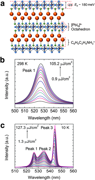 |
| | Fig. 1 Absence of ASE in PEPI. (a) Schematic structure of PEPI, which consists of alternating organic C6H5C2H4NH3+ and inorganic [PbI6]4− layers. The naturally formed quantum well structure enables the formation of tightly bound excitons with binding energy (Eb) ∼ 180 meV in the inorganic layers. (b) Room temperature pump fluence dependent PL spectrum of PEPI. (c) 10 K pump fluence dependent PL spectrum of PEPI showing three distinct emission peaks (peaks 1, 2 and 3). There is no superlinear increase in PL intensity for both temperatures. These optical experiments were conducted using 400 nm wavelength pump pulses (50 fs, 1 KHz). | |
PL peak assignments
Prior to modeling the recombination kinetics in PEPI, we need to establish the identities of peaks 1, 2 and 3 (see Fig. 1c). The identity of peak 1 is well established to originate from free exciton recombination. The energy of peak 1 remains almost unchanged with a slight unconventional red shift with decreasing temperature – Fig. 2a. The red-shifting behavior, which has previously been observed in 3D perovskite, can be attributed to effects from the negative Varshni parameter.23 Unfortunately, the origins of peaks 2 and 3 are still a matter of debate in the literature.
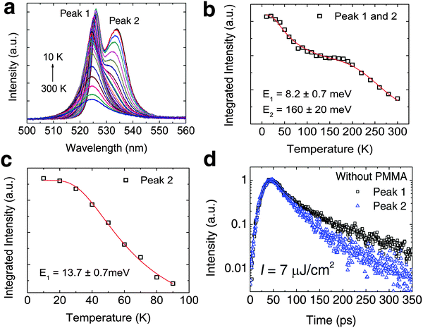 |
| | Fig. 2 Low temperature bound exciton formation in PEPI. (a) Temperature dependent PL spectrum of PEPI showing two distinct emission peaks (peaks 1 and 2). (b) Integrated PL intensity at different temperatures for peak 1 and peak 2. The plot is fitted with a biexponential Arrhenius equation:  Here, I is the integrated PL intensity, I0 is the integrated PL intensity at 0 K, A1 and A2 are the amplitudes, E1 and E2 are the activation energies, kB is the Boltzmann constant and T is the temperature. The larger energy (E1) is consistent with the exciton binding energy in PEPI. (c) Integrated PL intensity at different temperatures for peak 2. The small activation extracted with a single exponential Arrhenius equation is consistent with E1 in (b). (d) Lifetime of peak 1 and 2 emission. These optical experiments were conducted using 400 nm wavelength pump pulses (50 fs, 1 KHz, 2.6 μJ cm−2 (steady-state PL) or 7.0 μJ cm−2 (time-resolved PL)). Here, I is the integrated PL intensity, I0 is the integrated PL intensity at 0 K, A1 and A2 are the amplitudes, E1 and E2 are the activation energies, kB is the Boltzmann constant and T is the temperature. The larger energy (E1) is consistent with the exciton binding energy in PEPI. (c) Integrated PL intensity at different temperatures for peak 2. The small activation extracted with a single exponential Arrhenius equation is consistent with E1 in (b). (d) Lifetime of peak 1 and 2 emission. These optical experiments were conducted using 400 nm wavelength pump pulses (50 fs, 1 KHz, 2.6 μJ cm−2 (steady-state PL) or 7.0 μJ cm−2 (time-resolved PL)). | |
For peak 2, its origin was attributed to either a phonon replica or bound excitons. Gauthron et al.24 observed two low temperature PL peaks (peak 1 and peak X (2.337 eV or 530.5 nm, which is not observed by us)) and found a significant interaction between the free excitons (peak 1) and optical phonons from their phenomenological model. From the established relation between peak 1 and peak X, they attributed peak X to be a phonon replica of peak 1. Peak X (at 530.5 nm) observed by Gauthron et al. at 10 K need not correspond to peak 2 (535 nm) in our study. Furthermore, peak X also lacks the characteristic features of phonon replicas. On the other hand, Hong et al.25 observed multiple evenly spaced peaks (phonon replicas) at 2 K that are red-shifted from peak 1. However, Kitazawa et al.26 attributed a bound exciton origin to peak 2. They found a large characteristic exciton binding energy (∼200 meV) for (C6H5C2H4NH3)2PbI4 as well as a much smaller binding energy of ∼10 meV, which they attributed to the trapping–detrapping energy for bound excitons. This small energy is equivalent to a temperature of ∼120 K and corresponds well to the temperature at which peak 2 becomes prominent. These latter findings are consistent with our observations – Fig. 2b and c. In addition, the decay rates for peaks 1 and 2 (Fig. 2d) are different and this suggests that peak 2 is unlikely to be a phonon replica of peak 1. The bound exciton origin for this red-shifted peak was also evident in a similar 2-D perovskite ((C10H21NH3)2PbI4).27 Next, significant quenching of peak 2 at low temperatures (77 K and 10 K – see Fig. S5a and b, ESI†) is also observed after depositing a layer of PMMA on top of PEPI. The variable degrees of surface quenching for different sample batches at 77 K (see Fig. S5b, ESI†) suggest large surface trapping contribution to peak 2 with some bulk trapping contribution – implying the significant presence of surface bound excitons. The passivation of surface trapping on PEPI by PMMA is consistent with the broadening of peak 1 (i.e., free exciton peak), a PL intensity increase by ∼37% and free exciton lifetime lengthening at ∼10 K (see Fig. S5a, c and d, respectively, ESI†). X-ray photoelectron spectroscopy (XPS) revealed the presence of organic surface vacancies in PEPI (see Fig. S6 and Table S1, ESI†), which may be responsible for the surface trapping in PEPI. These findings suggest that surface trapping in PEPI cannot be neglected and could potentially have an adverse effect on the optical gain.
For peak 3 that appears at high excitation fluence, Shimizu et al. attributed the emission to originate from tri-excitons based on the 2.5 proportionality relation28,29 between the emission intensity and the excitation fluence. However, based on the quadratic increase in peak 3 emission with laser fluence at low temperatures, our result suggests a biexcitonic origin to peak 3 (see Fig. S7, ESI†). Such biexcitonic emission has also been previously reported for (C6H13NH3)2PbI4.17 The biexcitons in PEPI, with a binding energy of 40 meV (see the ESI† for biexciton binding energy determination), more likely reside at the surface as bound biexcitons since peak 3 is suppressed with significant quenching of peak 2 (see Fig. S8, ESI†).
In summary, our findings show that peak 1 originates from free excitons, peak 2 arises from surface bound excitons, and peak 3 from surface bound biexcitons.
Theoretical modeling of charge carrier relaxation
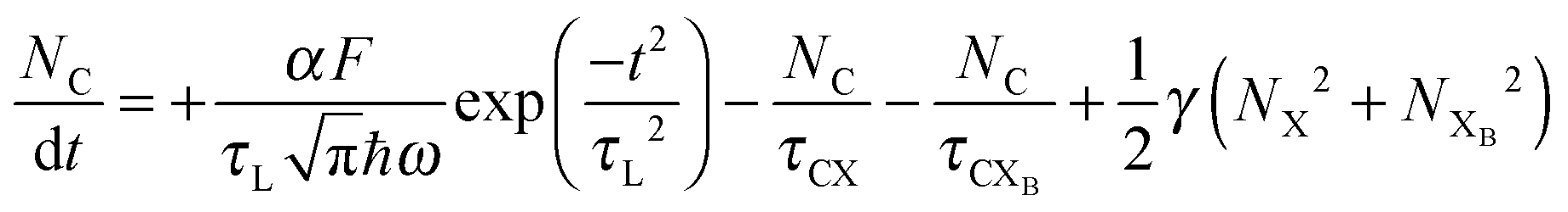
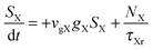
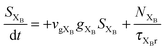
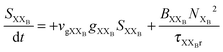
To investigate the factors affecting ASE in PEPI, we developed a model for carrier and emission dynamics in PEPI. This model is modified based on a well-established model of ASE in semiconductor nanostructures to account for our peak assignment.30 A schematic of the model is shown in Fig. 3a below, which comprises three emissive levels: free exciton, bound exciton and bound biexciton levels. This model involves the following relaxation processes following carrier excitation to the free carrier band |C〉: (1) formation of free excitons |X〉 and bound excitons |XB〉, (2) capture of free excitons from bound excitons, (3) non-radiative relaxation of free and bound excitons, (4) emission of free excitons, (5) emission of bound excitons, (6) formation and emission of bound biexcitons |XXB〉 and (7) non-radiative exciton–exciton annihilation. These processes are illustrated in Fig. 3a. From this model, the dynamics of the system are described by the following rate equations:| |  | (1) |
| |  | (2) |
| |  | (3) |
| |  | (4) |
| |  | (5) |
| |  | (6) |
The descriptions of the terms in eqn (1)–(6) are listed in Table 1. Meanwhile, the optical gain (g) is modeled by the competition between the absorption and the stimulated emission:| | | gXB = gXB0(2NXB/DX − 1) | (8) |
| | | gXXB = gXXB0(2BXXBNXB2/DX − 1) | (9) |
Here, the initial gain i.e., gX0, gXB0 and gXXB0 used are obtained from the linear absorption coefficient measurements, since gain =−absorption when N = 0. The density of states DX is estimated by the density of valence electrons of the lead cation, which is the main contributor for the valence states. The parameters used in this model are either taken from experimental parameters or obtained from experimental data (see Table S2, ESI†, for the parameters). The free exciton lifetime (peak 1) from the pristine PEPI film can be well-fitted with the numerical solution of eqn (3) – Fig. 4b. We also found that the numerical solution of eqn (1)–(3) as a function of laser pump fluence can be well-fitted by the deconvolved PL integrated intensity for the respective peaks – Fig. 3c. Our model also predicts an absence of ASE in the pump fluence range used in our studies – consistent with our experimental data. The behavior of the respective peaks is also extrapolated to the regime above the damage threshold (above the laser fluence range used) – Fig. 3c inset. Our model predicts an ASE onset for peak 3 at a laser fluence of 1.4 mJ cm−2 originating from biexcitonic ASE in PEPI. This value is approximately 1 order of magnitude higher than the experimental damage threshold. Here, we also explored the possibility of single excitonic gain.31 While the single excitonic gain in caesium lead halide perovskite QDs9 and in CdSe-based32 colloidal quantum dots have previously been proposed, such single excitonic ASE onsets are not experimentally observed for peak 1 (free exciton) and peak 2 (bound exciton) in the PEPI system. This is understandable from the model that the dominant competing relaxation channels in PEPI (i.e., free exciton to bound exciton relaxation and bound exciton to bound biexciton relaxation) would not favor the formation of metastable states. These competing channels are pre-requisites for the bound biexciton formation and for the subsequent bound biexciton gain build-up. Such competing channels are also not representative of a four-level lasing system found in excitonic organic semiconductor gain media.22
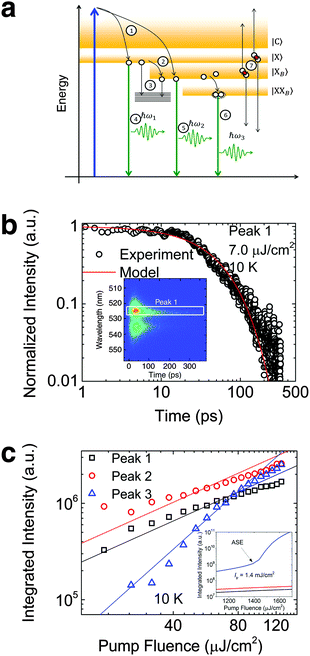 |
| | Fig. 3 Rate equation analysis of energetics and kinetics from PEPI. (a) Proposed schematics of the exciton (open circles) relaxation channels in PEPI. (b) 10 K TRPL kinetics of peak 1 emission from PEPI. The kinetics is well modeled using a set of rate equations described in eqn (1)–(6). Inset: 2D time-wavelength image of the PL emission with peak 1 labeled. The optical experiments were conducted using 400 nm wavelength pump pulses (50 fs, 1 KHz, 7 μJ cm−2). (c) Integrated PL intensity of the deconvolved peaks as a function of laser intensity extracted from Fig. 1c. The points are well-fitted using the proposed rate equations. Inset: Integrated PL intensity modeled at higher laser fluence with a predicted biexciton ASE threshold of 1.4 mJ cm−2. | |
| Parameter |
Description |
| ℏω |
Pump photon energy. |
|
α
|
Absorption coefficient at pump energy. |
|
τ
Xr
|
Exciton radiative lifetime. |
|
κ
Xnr
|
Exciton non-radiative relaxation rate. |
|
τ
XBr
|
Bound exciton non-radiative relaxation rate. |
|
κ
XBnr
|
Bound biexciton non-radiative relaxation rate. |
|
τ
XXr
|
Bound biexciton radiative relaxation rate. |
|
τ
CX
|
Free carrier to exciton relaxation time |
|
τ
CXB
|
Free carrier to bound exciton relaxation time |
|
τ
L
|
Laser time constant |
|
C
X
|
Bound exciton trapping |
|
B
XXB
|
Bound biexciton formation coefficient |
|
γ
|
Exciton–exciton annihilation coefficient |
|
v
gX
|
Group velocity at exciton emission energy |
|
v
gXB
|
Group velocity at bound exciton emission energy |
|
v
gXXB
|
Group velocity at bound biexciton emission energy |
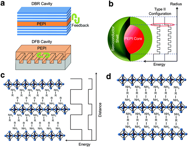 |
| | Fig. 4 Proposed strategies to promote optical gain. (a) Embedding 2D perovskite in a cavity (e.g. distributed Bragg reflector and distributed feedback cavity). Promoting single exciton gain using type II configuration by (b) surrounding 2D perovskite nanocrystals with a suitable semiconductor shell or (c) choosing an appropriate small bandgap organic constituent. (d) Employing a (H3N–R–NH3)PbI4 structure to improve film morphology which in turn may reduce trapping. | |
Proposed solutions to overcome the optical gain challenges
While AlInGaP and GaN materials have made electrically pumped red and blue lasers possible, a suitable candidate for green lasers is still elusive.19 Thus, overcoming the green gap in lasing still remains an important research area. If a suitable candidate is found, this could mean a huge breakthrough in the photonics industry. Conventional green lasing generated by frequency-doubling using a nonlinear crystal could then be replaced by a more efficient, directly generated green laser. In addition, high quality red, green and blue laser-based displays33 could also be made possible. Solution processed 2D perovskite systems exhibiting strong optically and electrically pumped spontaneous green emission could possibly contribute to the realization of electrically pumped green laser. However, achieving optical gain with these 2D materials has proven challenging. From the literature reports and our experimental results, we propose several key factors that may help to overcome the optical gain problem in 2D perovskites.
Managing exciton recombination losses is an important factor for achieving optical gain in 2D perovskites. From PL measurements, we establish that there is significant surface trapping in PEPI. The surface trapping gives rise to the formation of bound excitons (from free excitons) and bound biexcitons (from bound excitons). These competing pathways could be one of the reasons behind the lack of optical gain from biexcitons (formed directly by free excitons). As shown from our theoretical model, only bound biexcitonic gain can be achieved from this system. Unfortunately, this also means that these competing relaxation channels present cannot be eliminated for bound biexciton formation. These channels could cause losses and account for the calculated high bound biexcitonic ASE threshold of 1.4 mJ cm−2. A possible way to reduce loss and lower the ASE/lasing threshold would be to introduce an ultrahigh quality laser cavity (see Fig. 4a).
Enhancing excitonic gain through the use of 2D perovskite nanocrystals to induce optical gain could also be explored. Typical nanocrystal gain involves at least two excitons (biexciton), but the formation of biexcitons at high laser fluence can promote non-radiative Auger recombination. Klimov et al.31 had previously proposed a type-II core/shell configuration which employs the carrier-induced Stark effect to induce single exciton gain and eliminate Auger recombination. The carrier-induced Stark effect breaks the symmetry between absorption and emission by confining opposite charges in the core and the shell, respectively, thereby making the population inversion of single excitons possible. Similarly, a semiconductor shell surrounding 2D perovskite nanocrystals (core) can be used (see Fig. 4b). Building on this idea and with a careful choice of the organic component (R), a 2D perovskite thin film with type II electronic configuration34 could also be fabricated (see Fig. 4c) and may be useful for achieving single exciton gain. From our XPS data, the defects in PEPI were found to be from C and N deficiencies that could possibly originate from C–N bond breakage in the organic compound. Therefore using an organic component with a larger C–N bond dissociation energy may be helpful for reduction in trapping. Instead of using a (R–NH3)PbI4 structure where van der Waals forces exist between two ammonium units, a covalently bonded ammonium unit structure with the formula (NH3–R–NH3)PbI434 (see Fig. 4d) would be helpful. Strong covalently bonded constituents could lead to a better film morphology which can result in a further reduction in trapping.35
Conclusion
In retrospect, ultrafast spectroscopy provides a powerful means to probe exciton relaxation in PEPI. Regardless of excitation at low temperature or room temperature, no ASE could be observed in spin-coated PEPI thin films. Formation and relaxation of free excitons, bound excitons and biexcitons were found to be very dependent on each other. Theoretical modeling revealed a high bound biexciton ASE threshold beyond the damage threshold of PEPI, with no optical gain predicted from free and bound excitons. Several recommendations have also been proposed. A combination of these suggestions may be needed to overcome the optical gain challenge in 2D perovskites.
Conflicts of interest
The authors declare no competing financial interest.
Acknowledgements
Financial support from Nanyang Technological University start-up grants M4080514 and M4081293; the Ministry of Education AcRF Tier 1 grants RG184/14 and RG101/15 and Tier 2 grants MOE2013-T2-1-081 and MOE2014-T2-1-044; the NTU-A*STAR Silicon Technologies Center of Excellence Program Grant 11235100003 and from the Singapore National Research Foundation through the Singapore–Berkeley Research Initiative for Sustainable Energy (SinBeRISE) CREATE Program and the Competitive Research Program NRF-CRP14-2014-03 is gratefully acknowledged.
References
- H. Cho, S.-H. Jeong, M.-H. Park, Y.-H. Kim, C. Wolf, C.-L. Lee, J. H. Heo, A. Sadhanala, N. Myoung and S. Yoo,
et al.
, Science, 2015, 350, 1222–1225 CrossRef CAS PubMed.
- L. Dou, Y. Yang, J. You, Z. Hong, W.-H. Chang, G. Li and Y. Yang, Nat. Commun., 2014, 5, 5405 CrossRef PubMed.
- G. Xing, N. Mathews, S. S. Lim, N. Yantara, X. Liu, D. Sabba, M. Grätzel, S. Mhaisalkar and T. C. Sum, Nat. Mater., 2014, 13, 476–480 CrossRef CAS PubMed.
- H. Zhou, Q. Chen, G. Li, S. Luo, T.-b. Song, H.-S. Duan, Z. Hong, J. You, Y. Liu and Y. Yang, Science, 2014, 345, 542–546 CrossRef CAS PubMed.
- Y.-H. Kim, H. Cho, J. H. Heo, T.-S. Kim, N. Myoung, C.-L. Lee, S. H. Im and T.-W. Lee, Adv. Mater., 2015, 27, 1248–1254 CrossRef CAS PubMed.
- G. Li, Z.-K. Tan, D. Di, M. L. Lai, L. Jiang, J. H.-W. Lim, R. H. Friend and N. C. Greenham, Nano Lett., 2015, 15, 2640–2644 CrossRef CAS PubMed.
- Z.-K. Tan, R. S. Moghaddam, M. L. Lai, P. Docampo, R. Higler, F. Deschler, M. Price, A. Sadhanala, L. M. Pazos and D. Credgington,
et al.
, Nat. Nanotechnol., 2014, 9, 687–692 CrossRef CAS PubMed.
- Q. Zhang, S. T. Ha, X. Liu, T. C. Sum and Q. Xiong, Nano Lett., 2014, 14, 5995–6001 CrossRef CAS PubMed.
- S. Yakunin, L. Protesescu, F. Krieg, M. I. Bodnarchuk, G. Nedelcu, M. Humer, G. De Luca, M. Fiebig, W. Heiss and M. V. Kovalenko, Nat. Commun., 2015, 6, 8056 CrossRef CAS PubMed.
- H. Zhu, Y. Fu, F. Meng, X. Wu, Z. Gong, Q. Ding, M. V. Gustafsson, M. T. Trinh, S. Jin and X. Y. Zhu, Nat. Mater., 2015, 14, 636–642 CrossRef CAS PubMed.
- Y. Wang, X. Li, J. Song, L. Xiao, H. Zeng and H. Sun, Adv. Mater., 2015, 27, 7101–7108 CrossRef CAS PubMed.
- I. Koutselas, P. Bampoulis, E. Maratou, T. Evagelinou, G. Pagona and G. C. Papavassiliou, J. Phys. Chem. C, 2011, 115, 8475–8483 CAS.
- M. Era, S. Morimoto, T. Tsutsui and S. Saito, Appl. Phys. Lett., 1994, 65, 676–678 CrossRef CAS.
- T. Hattori, T. Taira, M. Era, T. Tsutsui and S. Saito, Chem. Phys. Lett., 1996, 254, 103–108 CrossRef CAS.
- M. Era, T. Ano and M. Noto, Stud. Interface Sci., 2001, 11, 165–173 CAS.
- K. Chondroudis and D. B. Mitzi, Chem. Mater., 1999, 11, 3028–3030 CrossRef CAS.
- T. Kondo, T. Azuma, T. Yuasa and R. Ito, Solid State Commun., 1998, 105, 253–255 CrossRef CAS.
- I. D. W. Samuel, E. B. Namdas and G. A. Turnbull, Nat. Photonics, 2009, 3, 546–549 CrossRef CAS.
- Editorial, Filling the green gap, Nat. Photonics, 2009, 3, 421, DOI:10.1038/nphoton.2009.118.
- M. Coelle, W. Bruetting, M. Schwoerer, M. Yahiro and T. Tsutsui, Proc. SPIE, 2001, 4105, 328, DOI:10.1117/12.416912.
- X. Y. Chin, D. Cortecchia, J. Yin, A. Bruno and C. Soci, Nat. Commun., 2015, 6, 7383 CrossRef CAS PubMed.
-
Y. Wang, Low Threshold Organic Semiconductor Lasers, Springer, 2014, pp. 9–32 Search PubMed.
- W. Zhang, M. Saliba, S. D. Stranks, Y. Sun, X. Shi, U. Wiesner and H. J. Snaith, Nano Lett., 2013, 13, 4505–4510 CrossRef CAS PubMed.
- K. Gauthron, J. Lauret, L. Doyennette, G. Lanty, A. Al Choueiry, S. Zhang, A. Brehier, L. Largeau, O. Mauguin and J. Bloch, Opt. Express, 2010, 18, 5912–5919 CrossRef CAS PubMed.
- X. Hong, T. Ishihara and A. V. Nurmikko, Phys. Rev. B: Condens. Matter Mater. Phys., 1992, 45, 6961 CrossRef CAS.
- N. Kitazawa, M. Aono and Y. Watanabe, Mater. Chem. Phys., 2012, 134, 875–880 CrossRef CAS.
- T. Ishihara, J. Takahashi and T. Goto, Solid State Commun., 1989, 69, 933–936 CrossRef CAS.
- M. Shimizu, J.-i. Fujisawa and T. Ishihara, Phys. Rev. B: Condens. Matter Mater. Phys., 2006, 74, 155206 CrossRef.
- M. Shimizu, J.-i. Fujisawa and T. Ishihara, J. Lumin., 2007, 122, 485–487 CrossRef.
- D. Saxena, S. Mokkapati, P. Parkinson, N. Jiang, Q. Gao, H. H. Tan and C. Jagadish, Nat. Photonics, 2013, 7, 963–968 CrossRef CAS.
- V. I. Klimov, S. A. Ivanov, J. Nanda, M. Achermann, I. Bezel, J. A. McGuire and A. Piryatinski, Nature, 2007, 447, 441–446 CrossRef CAS PubMed.
- C. Dang, J. Lee, C. Breen, J. S. Steckel, S. Coe-Sullivan and A. Nurmikko, Nat. Nanotechnol., 2012, 7, 335–339 CrossRef CAS PubMed.
- F. Fan, S. Turkdogan, Z. Liu, D. Shelhammer and C. Z. Ning, Nat. Nanotechnol., 2015, 10, 796–803 CrossRef CAS PubMed.
- D. B. Mitzi, K. Chondroudis and C. R. Kagan, IBM J. Res. Dev., 2001, 45, 29–45 CrossRef CAS.
- S. Zhang, P. Audebert, Y. Wei, A. Al Choueiry, G. Lanty, A. Bréhier, L. Galmiche, G. Clavier, C. Boissière, J.-S. Lauret and E. Deleporte, Materials, 2010, 3, 3385 CrossRef CAS.
Footnote |
| † Electronic supplementary information (ESI) available: Statistics of perovskite optical gain reports, typical lasing evidence, physical characterization (XRD, SEM and steady state absorption), damage threshold determination, effects of PMMA on the PEPI PL spectrum, XPS surface composition ratio, and parameters of the rate equations. See DOI: 10.1039/c6cp01955b |
|
| This journal is © the Owner Societies 2016 |

 Open Access Article
 This Open Access Article is licensed under a

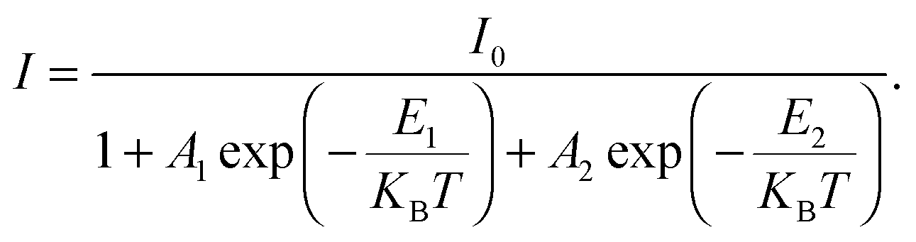 Here, I is the integrated PL intensity, I0 is the integrated PL intensity at 0 K, A1 and A2 are the amplitudes, E1 and E2 are the activation energies, kB is the Boltzmann constant and T is the temperature. The larger energy (E1) is consistent with the exciton binding energy in PEPI. (c) Integrated PL intensity at different temperatures for peak 2. The small activation extracted with a single exponential Arrhenius equation is consistent with E1 in (b). (d) Lifetime of peak 1 and 2 emission. These optical experiments were conducted using 400 nm wavelength pump pulses (50 fs, 1 KHz, 2.6 μJ cm−2 (steady-state PL) or 7.0 μJ cm−2 (time-resolved PL)).