
 Open Access Article
 This Open Access Article is licensed under a
 Creative Commons Attribution 3.0 Unported Licence
A comprehensive comparison of dye-sensitized NiO photocathodes for solar energy conversion†
Christopher J.
Wood‡
a,
Gareth H.
Summers‡
a,
Charlotte A.
Clark
a,
Nicolas
Kaeffer
b,
Maximilian
Braeutigam
cd,
Lea Roberta
Carbone
e,
Luca
D'Amario
f,
Ke
Fan
g,
Yoann
Farré
h,
Stéphanie
Narbey
i,
Frédéric
Oswald
i,
Lee A.
Stevens
j,
Christopher D. J.
Parmenter
k,
Michael W.
Fay
k,
Alessandro
La Torre
k,
Colin E.
Snape
l,
Benjamin
Dietzek
cd,
Danilo
Dini
e,
Leif
Hammarström
f,
Yann
Pellegrin
h,
Fabrice
Odobel
h,
Licheng
Sun
g,
Vincent
Artero
b and
Elizabeth A.
Gibson‡
*a
aSchool of Chemistry, The University of Nottingham, University Park, Nottingham, NG7 2RD, UK
bLaboratoire de Chimie et Biologie des Métaux, Université Grenoble Alpes, CEA, CNRS, 17 rue des Martyrs, 38000 Grenoble, France
cInstitute of Photonic Technology (IPHT) Jena e. V., Albert-Einstein-Straße 9, D-07745 Jena, Germany
dInstitute for Physical Chemistry and Abbe Center of Photonics, Friedrich-Schiller University Jena, Helmholtzweg 4, D-07743 Jena, Germany
eDepartment of Chemistry, University of Rome “La Sapienza”, Rome, Italy
fDepartment of Chemistry-Ångström, Uppsala University, Box 259, SE-751 05 Uppsala, Sweden
gSchool of Chemical Science and Engineering, Royal Institute of Technology (KTH), 100 44 Stockholm, Sweden
hCEISAM, Chimie et Interdisciplinarité, Synthèse, Analyse, Modélisation, CNRS, UMR 6230, Faculté des Sciences et des Techniques Université de Nantes, 2, rue de la Houssinière, BP 92208, 44322 NANTES Cedex 3, France
iSolaronix, rue de l'Ouriette 129, CH-1170 Aubonne, Switzerland
jDivision of Materials, Mechanics and Structures, Faculty of Engineering, University of Nottingham, University Park, Nottingham, NG7 2RD, UK
kNottingham Nanotechnology and Nanoscience Centre, University of Nottingham, University Park, Nottingham, NG7 2RD, UK
lDepartment of Chemical and Environmental Engineering, Faculty of Engineering, University of Nottingham, University Park, Nottingham, NG7 2RD, UK
First published on 22nd December 2015
Abstract
We investigated a range of different mesoporous NiO electrodes prepared by different research groups and private firms in Europe to determine the parameters which influence good quality photoelectrochemical devices. This benchmarking study aims to solve some of the discrepancies in the literature regarding the performance of p-DSCs due to differences in the quality of the device fabrication. The information obtained will lay the foundation for future photocatalytic systems based on sensitized NiO so that new dyes and catalysts can be tested with a standardized material. The textural and electrochemical properties of the semiconducting material are key to the performance of photocathodes. We found that both commercial and non-commercial NiO gave promising solar cell and water-splitting devices. The NiO samples which had the two highest solar cell efficiency (0.145% and 0.089%) also gave the best overall theoretical H2 conversion.
Introduction
Since He et al. reported the first dye-sensitized NiO photocathode and assembled it in a tandem dye-sensitized solar cell, an opportunity to increase the efficiency of solar energy conversion in photoelectrochemical devices has been recognised.1,2 Firstly, the theoretical maximum efficiency of dye-sensitized solar cells (DSCs) is increased from 33% to 43% by replacing the platinized counter electrode in conventional DSC with a photocathode such as dye-sensitized NiO (Fig. 1a). Secondly, the redox electrolyte which completes the circuit in a photoelectrochemical solar cell (i.e. a DSC) can be replaced with water so that hydrogen can be generated at the photocathode and oxygen can be formed at the photoanode (Fig. 1b). This dye-sensitized photoelectrosynthetic cell (DPEC)3 can produce hydrogen as a solar fuel while avoiding the requirement for sacrificial agents which are usually required in photocatalytic approaches.3–5 In such architectures, catalysts, either molecular or materials, are usually required to facilitate water splitting into hydrogen and oxygen. Both types of device are relatively new concepts and the efficiency of the devices that have been reported is very low (2.42% efficiency for a tandem DSC6 compared to 13% efficiency for the state of the art TiO2-based DSCs;7 maximum incident photon-to-current efficiencies up to 15% in TiO2-based DPECs8 compared to 0.6% for NiO-based DPECs9). Therefore the efficiency of tandem photoelectrochemical devices is limited by the performance of the photocathode. A breakthrough in this area is anticipated if highly efficient p-type photocathodes can be realised.10 | ||
| Fig. 1 Schematic illustration of (a) a tandem dye-sensitized solar cell and (b) a dye-sensitized photoelectrosynthetic cell. (VB: valence band; CB: conduction band; HEC: hydrogen evolution catalyst; OEC: oxygen evolution catalyst). | ||
Recently, the performance of NiO-based DSCs were reviewed in the context of the preparation method used for the mesoporous electrode.11 It was observed that surface morphology is of primary importance to control the oxidation properties of NiO. The presence of defects is important to the performance of the device, especially the recombination reactions (2) and (3) in Fig. 1(a). The most efficient devices that have been reported were prepared from pre-formed NiO nanoparticles and companies such as Solaronix and Dyenamo are now selling screen-printable pastes. However, it is difficult to assess from the literature whether the source of NiO is important compared to other factors such as the device assembly method, choice of dye and sensitization conditions etc. we took the opportunity of the COST Action CM1202 on Supramolecular water splitting to organise a workshop for the benchmarking of different NiO electrodes, prepared in different research groups in Europe from lab-made or commercial sources, in DSCs and DPECs under the same conditions. This was designed to answer questions such as whether the control over the purity and crystallinity achieved by preparing the particles in house is preferential to purchasing NiO nanoparticles or commercial paste; whether the trends observed in DSCs can be translated directly to the performance of water-splitting DPECs.
The experiments were chosen so that the chemical-physical properties such as crystal size, BET surface area and electrochemical properties could be compared to the DSC and DPEC device performance. The dye P1 (Fig. 2) was chosen because it has been used in both p-type DSCs and DPECs.12,13 The I3−/I− electrolyte for the DSCs was chosen because this redox couple is known to be optimised for this dye.14 The [Co(dmgBF2)2(H2O)2] (dmg2−: dimethylglyoximato dianion) hydrogen evolving catalyst was chosen for the DPEC because it has been extensively characterised elsewhere and because Li et al. demonstrated that it can be incorporated into a P1-sensitized NiO DPEC to reduce protons.8,15 In the devices, absorption of visible light by P1 leads to electron transfer from NiO to the dye. The potential of the reduced dye (−0.93 V vs. NHE)16 is sufficient to reduce I3− to I− or [Co(dmgBF2)2(H2O)2] both from the Co(II) to the Co(I) state, the entry point of the catalytic proton reduction cycle, and further from the Co(III)–H to form the active Co(II)–H species.17–19
 | ||
| Fig. 2 Energy diagram of NiO-P1-[Co(dmgBF2)2(H2O)2] electrodes (note: potentials of P1 in MeCN from Qin et al.16 and for [Co(dmgBF2)2(H2O)2] in pH 7 phosphate buffer corrected vs. NHE from Berben et al.20). TCL: transparent conducting layer. | ||
Experimental
Sample preparation
Sample 1a/1b was prepared by following the method according to Grätzel for TiO2.21Sample 2 was prepared by grinding 3 g of NiO ground in planetary mill (500 rpm) for 24 h with EtOH. 10 mL of ethyl cellulose 10% in EtOH, 20 mL terpineol were added and the EtOH was removed under vacuum. The paste was deposited onto FTO glass by screen printing. The electrodes were sintered according to the following program:
Sample 3 was prepared according to Bräutigam et al.22 Minor alterations included the deposition by doctor blading and the 3-fold repetition of this to yield thicker NiO surfaces.
Sample 4 conducting glass substrates were cut to size and then cleaned in an ultrasonic bath for 15 minutes, first in soapy water, second in propan-2-ol and finally in acetone. The NiO precursor solution was prepared by dissolving anhydrous NiCl2 (1 g) and the tri-block co-polymer F108 (poly(ethylene glycol)-block-poly(propylene glycol)-block-poly(ethylene glycol)) (1 g) in ethanol (6 g) and ultrapure Milli-Q water (5 g).23 NiO electrodes were made by applying the precursor solution onto conducting glass substrates (Pilkington TEC15, sheet resistance 15 Ω sq−1) by doctor blade using Scotch tape as a spacer (0.2 cm2 active area), followed by sintering in a Nabertherm B150 oven at 450 °C for 30 min.
Samples 5a–d were purchased from Dyenamo, where they are prepared by screen printing (one layer for sample a and b and two layers for samples c and d). The as-received plates were sintered in a flat oven (PZ28-3TD, Harry Gestigkeit) monitored by a controller (Programmer PR5, Detlef Gestigkeit) applying the following temperature gradients:
– For samples a and c: from r.t. to 350 °C in 30 min; 30 min at 350 °C; gently back to r.t.
– For samples b and d: from r.t. to 450 °C in 30 min; 30 min at 450 °C; gently back to r.t.
Samples 5e,f were prepared by Solaronix by screen printing of a NiO paste (Ni-Noxide N/SP). The as-received plates were sintered in a flat oven (PZ28-3TD, Harry Gestigkeit) monitored by a controller (Programmer PR5, Detlef Gestigkeit) applying the following temperature gradients:
– For samples e: from r.t. to 350 °C in 30 min; 30 min at 350 °C; gently back to r.t.
– For samples f: from r.t. to 450 °C in 30 min; 30 min at 450 °C; gently back to r.t.
Samples 6a–c were prepared according to D'Amario et al.24 3 g of anhydrous NiCl2 and 3 g of F108 polymer were dissolved in a mixture of deionized water (9 g) and 99.5% ethanol (18 g). The resulting green viscous solution was sonicated overnight. The mixture was centrifuged for 15 min to sediment out undissolved NiCl2 and amorphous NiO. After centrifugation, the supernatant was collected as four separate batches for use as doctor-blading paste. The Li-doping was carried out by adding 0, 0.1 and 0.5 mol% of LiCl to the NiCl2 sol–gel. The LiCl was added by water solution using less than 1% of the final batch volume. Then, the mixture was stirred for 1 day. Mesoporous NiO electrodes were prepared by spreading the doctor-blading paste onto FTO glass masked with adhesive tape and sintered in a furnace at 450 °C for 30 min.
Sample 7 commercial NiO nanoparticles (1.0 g, 20 nm Inframat Advanced Materials) were mixed with of ethanol (8.0 mL), acetic acid (0.2 mL), terpinol (3.0 g) and ethyl cellulose (0.5 g) by ball-milling for 2 h. The obtained paste was screen-printed on clean FTO glass, followed by sintering at 450 °C in air for 30 min (Table 2).
| Start temperature (°C) | End temperature (°C) | Ramp | Time at fixed temperature | |
|---|---|---|---|---|
| 1 | RT | 110 | 30 min | 30 min |
| 2 | 110 | 250 | 1 h | 30 min |
| 3 | 250 | 340 | 15 min | 5 min |
| 4 | 340 | 400 | 30 min | 30 min |
| Sample | Deposition | Area (cm2) | Type | Sintering | Thickness (μm) | |
|---|---|---|---|---|---|---|
| Ramp | Final | |||||
| a Measured from SEM cross sectional images. b Measured using a Dektak Profilometer. | ||||||
| 1a | Screen print | 0.25 | Aldrich nanoparticles (around 20 nm) | 40 min ramp r.t. to 550 °C | 30 min@550 °C | 2b |
| 1b | 0.25 | Aldrich nanoparticles (around 20 nm) | 40 min ramp r.t. to 550 °C | 30 min@550 °C | 5b | |
| 2 | Screen print | 0.36 | Inframat nanoparticles (around 20 nm) | (See Table 1) | 1.4a | |
| 3 | Doctor blade 3 layers | 0.36 | Copolymer PS-b-P2VP | 30 min@450 °C | 0.2a | |
| 4 | Doctor blade | 0.20 | F108 | 30 min ramp r.t. to 450 °C | 30 min@450 °C | 0.83b |
| 5a | Screen print 1 layer | 0.46 | Dyenamo | 30 min ramp r.t. to 350 °C | 30 min@350 °C | 0.74a |
| 5b | 0.44 | 30 min ramp r.t. to 450 °C | 30 min@450 °C | |||
| 5c | Screen print 2 layers | 0.37 | 30 min ramp r.t. to 350 °C | 30 min@350 °C | 1.75a | |
| 5d | 0.26 | 30 min ramp r.t. to 450 °C | 30 min@450 °C | |||
| 5e | Screen print 1 layer | 0.41 | Solaronix | 30 min ramp r.t. to 350 °C | 30 min@350 °C | |
| 5f | 0.37 | 30 min ramp r.t. to 450 °C | 30 min@450 °C | |||
| 6a | Doctor blade | 0.25 | 0% Li-doped F108 | 30 min@450 °C | 0.70 ± 0.05b | |
| 6b | 0.1% Li-doped F108 | |||||
| 6c | 0.5% Li-doped F108 | |||||
| 7 | Screen print 1 layer | Inframat nanoparticles (around 20 nm) | 30 min@450 °C | |||
Electron microscopy
SEM micrographs for 5e and f were recorded using a FEI Quanta200 3D DualBeam FIB/SEM. High resolution TEM was recorded using the JEOL 2100F TEM equipped with a JEOL digital STEM system and a Gatan Tridiem spectrometer at the Nottingham Nanoscience and Nanotechnology Centre. The NiO was removed from the FTO glass and loaded onto a carbon coated copper TEM grid (Agar Scientific).Powder X-ray diffraction (PXRD)
PXRD patterns were collected at room temperature in the 10°–80° range on a PANanalytical Multi-purpose Diffractometer operated at 40 kV and 40 mA (Cu Kα1, λ = 1.5406 Å). Powder samples were deposited from a slurry in ethanol onto a silicon zero diffraction plate and NiO films on FTO were prepared as described above. The data was analysed using PANanalytical X'Pert Highscore.Kr gas adsorption isotherms
Adsorption isotherms were carried out by using a Micromeritics ASAP 2420 (Micromeritics, Norcross, GA, USA) using krypton as the adsorbate. NiO samples were prepared as described above onto ca. 0.5 cm × 1 cm FTO glass substrates. Three replicates of each sample were inserted into glass sample tubes with a sealed frit. The samples were degassed under vacuum at 25 °C for 3 hours to remove moisture and other adsorbed gases. Krypton isotherms were acquired from 0.07–0.25 relative pressure (p/p0) at −195.85 °C in liquid nitrogen (N2). The glass samples were then weighed and reweighed following the removal of the NiO in order to give an accurate sample weight. The BET model for specific surface area was fitted to the Kr isotherms using Microactive V3.0 software (Micrometrics Instrument Corporation).Electrochemistry
Cyclic voltammetry was carried out using a Palmsens Emstat potentiostat. A three electrode system was used with the NiO film working electrode, a Ag/Ag+ (Sat. AgCl in 3 M NaCl(aq)) reference electrode and a Pt wire counter electrode immersed in pH 7 buffer solution.Solar cells
The NiO electrodes were soaked in an acetonitrile solution of P1 (0.3 mM) for 16 h at room temperature. The dyed NiO electrode was assembled face-to-face with a platinized counter electrode (Pilkington TEC8, sheet resistance 8 Ω sq−1) using a 30 μm thick thermoplastic frame (Surlyn 1702). Then the electrolyte, containing LiI (1.0 M) and I2 (0.1 M) in acetonitrile, was introduced through the pre-drilled hole in the counter electrode, which was sealed afterwards. The UV-visible absorption spectra of the dyes adsorbed on NiO films were recorded using an Ocean Optics USB2000 + VIS-NIR fibre-optic spectrophotometer. Current–voltage measurements were measured using an Ivium CompactStat potentiostat under AM1.5 simulated sunlight from an Oriel 150 W solar simulator, giving light with an intensity of 100 mW cm−2. Incident photon-to-current conversion efficiency curves (IPCE) were recorded by passing the light from the solar simulator through an Oriel Cornerstone 130 1/8m monochromator and recording the current from the solar cell with an Ivium CompactStat potentiostat which was calibrated against a Si photodiode.Small amplitude square wave modulated (SSWM) photovoltage and photocurrent experiments were performed on the same p-DSCs used for the J–V and IPCE measurements at open circuit and short circuit, respectively. SSWM experiments were carried out over a range of light intensities, using an Ivium Modulight as a modulated light source with a 10% modulation of light intensity. The photovoltage and photocurrent rise and decays were recorded using an Ivium CompactStat potentiostat, the lifetimes were fitted to a 1st order exponential decay using Origin Pro 8. Charge extraction was performed using the same equipment, the cell was illuminated at open-circuit until a constant VOC was reached, the light source was then switched off allowing for a decay in photovoltage, over a range of time intervals. Following this the cell was switched to short-circuit conditions and the current decay over 10 seconds was integrated to give the charge at varying photovoltages.
Photoelectrochemical measurements
For the electrochemical measurements a custom-built three compartment cell was used. A Pt wire (0.5 mm) counter electrode and a Ag/AgCl reference electrode were employed. The working electrode for each experiment were typically prepared on TEC 15 FTO glass with areas ranging between 0.636–0.25 cm2. The sample preparation for each electrode was identical: (1) the NiO films were soaked in a CH3CN dye bath containing P1 (0.3 mM) for a period of 12 h. (2) The films were rinsed in CH3CN to remove unadsorbed dye. (3) Finally, the co-catalyst [CoII(dmg-BF2)2(OH)2] was introduced by slow drop-casting 100 μL of a 2 mM solution in CH3CN and the sample was dried in air.The electrolyte used in all experiments was an aqueous solution containing 50 mM phosphate at pH 7. All solutions were degassed by bubbling with Ar for a minimum of 5 minutes prior to commencing of the experiment and Ar was continually bubbled through the solution using a Bronkhorst flow-controller (flow rate = 10 mL min−1) throughout the measurement. A 200 μL sample of the Ar flowing out from the cell was analyzed automatically every 3 min using a gas chromatograph (Shimadzu 2014) with a thermal conductivity detector operating at 50 °C. There was insufficient H2 produced in the cell to quantify it accurately using this method. The visible LED used for photolysis is an OSRAM® OSTAR® white LED with an output of 1000 lm. Care was taken to place the LED in an identical position for each measurement. A constant potential of −0.4 V vs. Ag/AgCl was applied during each experiment and the current measured using an EmStat potentiostat.
Results and discussion
Film morphology
All the NiO samples were based on nanoparticles prepared either in situ or pre formed and applied as a paste using a combination of organic surfactants and binders. Full details are given in the Experimental section and the corresponding references. In general the particle shape and film morphology was similar for each sample. SEM for 1 can be found in ref. 34. SEM images for samples 2 and 5b and d are provided in Fig. 3. High resolution TEM for 5e–f are shown in Fig. 4. SEM images for the sol–gel prepared films 3, 4 and 6 have previously been reported in ref. 12, 20 and 22 respectively and high resolution TEM images for 4 are provided in Fig. 4.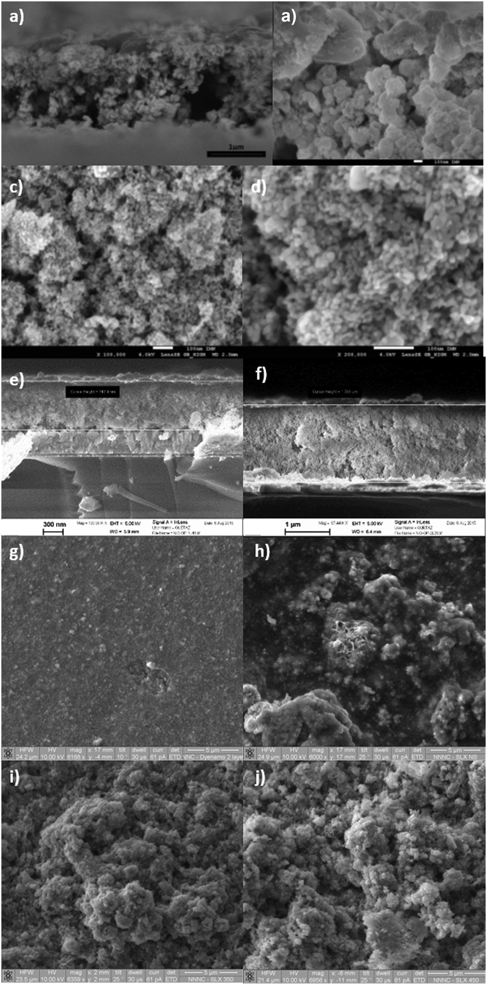 | ||
Fig. 3 SEM micrographs of (a), (b) the cross-section of 2 (50![[thin space (1/6-em)]](https://www.rsc.org/images/entities/char_2009.gif) 000× magnification); (c) the surface morphology of 2 (100000×), (d) the surface morphology of 2 (200000×), (e) the cross section of 5b (100000×); (f) the cross section of 5d (67000×); (g) the surface of 5b (6000×); (h) the surface of a film made from the Solaronix paste before sintering (6000×); (i) the surface of 5e (6000×); (j) the surface of 5f (7000×). HV = 5 kV (for sample 2), 4 kV (5b, 5d) 10 kV (5e, 5f). WD = 2–5 mm. 000× magnification); (c) the surface morphology of 2 (100000×), (d) the surface morphology of 2 (200000×), (e) the cross section of 5b (100000×); (f) the cross section of 5d (67000×); (g) the surface of 5b (6000×); (h) the surface of a film made from the Solaronix paste before sintering (6000×); (i) the surface of 5e (6000×); (j) the surface of 5f (7000×). HV = 5 kV (for sample 2), 4 kV (5b, 5d) 10 kV (5e, 5f). WD = 2–5 mm. | ||
 | ||
| Fig. 4 High resolution TEM micrographs of (a) 1, (b) 4, (c) 5e and (d) 5f at 50000× magnification. | ||
Powder X-ray diffraction (PXRD)
The undyed NiO films were characterised using powder X-ray diffraction both for the samples on FTO and for the nanoparticles removed from the glass substrate. A representative X-ray diffraction pattern for the film on FTO (Fig. 5a) and the powder removed from the film (Fig. 5b) are given below. | ||
| Fig. 5 Representative X-ray diffraction patterns for sample 4: (a) the NiO film on FTO; (b) the NiO nanoparticles removed from the film. The diffraction peaks indexed with the (hkl) notation correspond to the main NiO phase.25 * Denotes the peaks corresponding to NiO. | ||
The results of the XRD analysis are summarised in Table 3 for the film and powder respectively. The mean crystallite size estimated from the major diffractions ranged from 10 to 20 nm. Generally as the sintering temperature increases the mean crystallite size also increases, with the smallest being 10 nm for 5e corresponding to a sintering temperature of 350 °C while the larger samples of 16 (1a) and 21 nm (4) were sintered at 550 and 450 °C respectively. For the screen printed pastes (7, 5d, 1a) sintered at 450 °C the mean crystallite sizes were fairly consistent and within the range of 13–16 nm while generally the NiO films made via a sol–gel process (6, 3) were within the range of 12–14 nm which is smaller than for the screen printed pastes. The difference in crystallite size for the two films made via a sol–gel process using F108 (21 nm for the undoped film, 4, to 12 nm with 0.5% Li, 6) are attributed to the different solvent ratio in the precursor solution. The crystallite size in the Li-doped film 6 is in agreement with previously reported results by Sumikura et al. (12 nm with F108) and a slightly larger crystallite size was reported by Li et al. (16 nm).12,23 Differences of around 1 nm were observed when comparing the mean crystallite size of the NiO films on FTO and the nanoparticles removed from the glass substrate. However, rather than a change in morphology this has been attributed to improved resolution for the measurement on the silicon zero diffraction plate (Fig. 5b) compared to the NiO on FTO (Fig. 5a) where there is a significant overlap of the diffractions from NiO and SnO2.
| Sample | BET surface areaa (m2 g−1) | Mean crystallite sizeb,c (nm) |
|---|---|---|
| a BET specific surface areas obtained from Krypton adsorption isotherms. b Average mean crystallite size for NiO films on FTO, calculated using the Scherrer equation. c In parentheses, average mean crystallite size for NiO nanoparticles. | ||
| 1 | 21.46 ± 0.07 | 16.1 |
| 2 | — | (14.0) |
| 3 | 7.71 ± 0.45 | 13 |
| 4 | 40.56 ± 0.19 | 20.6 (19.7) |
| 5a | 41.79 ± 0.71 | (17) |
| 5c | 39.36 ± 0.77 | — |
| 5d | 70.92 ± 0.58 | 15.4 |
| 5e | 63.15 ± 0.46 | 9.9 |
| 6a | 24.46 ± 0.70 | — |
| 6b | 31.28 ± 0.44 | — |
| 6c | 22.17 ± 0.54 | 11.5 |
| 7 | 60.48 ± 0.17 | 13.7 (14.8) |
This is most apparent for the thinner films (see ESI†) where the NiO diffractions were very low in intensity compared to those from SnO2. Interestingly the crystallite size for samples 1, 2 and 7 prepared from commercial NiO was less than the advertised average particle size of 20 nm. Samples 2 and 7, which both contain Inframant NiO, agreed within 1 nm.
Kr gas adsorption
A summary of the surface areas obtained from Kr adsorption isotherms is given in Table 3 and examples of adsorption isotherms for samples 5c and 5d, as well as 3 and 4, respectively, are given in Fig. 6. All samples gave BET surfaces areas within an order of magnitude (7–70 m2 g−1). NiO screen printing pastes Dyenamo (5d), Solaronix (5e), typically had the highest surface areas (60–70 m2 g−1). There was a significant difference in the surface areas obtained from the NiO films with commercial NiO nanoparticles, 1b (Sigma Aldrich) and 7 (Inframat). The highest surface area was obtained with 5d which was prepared from the Dyenamo NiO paste and sintered at 450 °C (71 m2 g−1). As shown in Fig. 6, this was significantly higher than the surface area obtained for 5c sintered at 350 °C (39 m2 g−1) and it demonstrates the importance of temperature on the formation of NiO films. Here we attribute the lower surface area for the film sintered at lower temperature to incomplete combustion of the organic binders. However, sample 5e made from the Solaronix screen printing paste and sintered 350 °C had a comparatively high surface area (63 m2 g−1). Unfortunately it was not possible to acquire gas adsorption for this paste sintered at 450 °C. In sol–gel NiO films, higher temperature are required to ensure the all the polymer template has been removed.23 A study by Bach et al. demonstrated that sintering at higher temperatures (550 °C) improves the crystallinity but can lead to a large drop in the surface area (122 m2 g−1 for unsintered NiO, 56 m2 g−1 for 10 minutes at 550 °C and 12 m2 g−1 for 200 minutes at 550 °C).26 This may explain the difference between samples 1b and 7 made from commercial nanoparticles.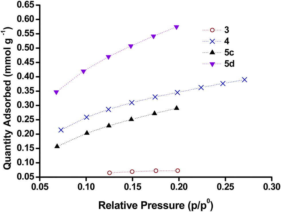 | ||
| Fig. 6 Kr gas adsorption for NiO films made from NiO films made from sol–gel methods with different block copolymers, 4 (blue) and 3 (brown) and Dyenamo NiO paste and sintered at 350 °C (5c, black) and 450 °C (5d, purple). | ||
Also shown in Fig. 6 is the Kr adsorption for samples 3 and 4 which were prepared by sol–gel routes. The surface areas for the samples prepared from sol–gel methods were generally lower than those obtained from pre-formed NiO nanoparticles. The BET surface area of 4 was in agreement with the N2 BET for NiO prepared by the same method reported by Sumikura et al.23 However, the sample 6a, which was prepared from the same method had a significantly lower surface area (24 m2 g−1). The sol–gel samples prepared using a polystyrene-block-poly(2-vinylpyridine) diblock copolymer template (3) gave the lowest surface area (7.7 m2 g−1). This value was significantly lower than the values for this sample using N2 as the adsorbate as reported previously by Bräutigam et al. (ca. 50 m2 g−1).22 Yet, we note that the preparation method for these samples has been slightly altered from the literature (cf. experimental part).
Cyclic voltammetry
Cyclic voltammetry (CV) was performed in a 50 mM phosphate buffer electrolyte at pH 7 with a scan rate of 20 mV s−1. Two characteristic broad but distinct peaks can be observed in the anodic and cathodic scans for all the NiO electrodes including the Li-doped NiO sample 6b. The peak current density and peak area in the voltammograms of the six NiO films shown in Fig. 7 differed greatly. The peak current density for both processes (and area under the peaks) was highest for the screen-printed NiO films 5d and 7 (150–200 μA cm−2), while 1b and 3 exhibited very low redox peaks (less than 50 μA cm−2). As a higher specific surface area leads to more active sites exposed to the electrolyte where electron transfer can take place, the magnitude of the peak area should be related to the specific surface area of the film. The results from the cyclic voltammetry were in agreement with the BET surface area (vide supra), for example, 5a and 7 have the highest BET surface, while the surface area of 1b and 3 were much lower. The matching trend in increasing peak area with increasing surface area is consistent with redox chemistry occurring at the surface of the electrodes.27 | ||
| Fig. 7 Cyclic voltammograms of the different NiO preparations, recorded in phosphate buffer (0.05 M pH 7) at a scan rate of 20 mV s−1. | ||
The two peaks have previously been attributed to Ni2+/Ni3+ (peak A) and Ni3+/Ni4+ (peak B), respectively.11 However, if all the Ni atoms were first oxidized to Ni3+, and then to Ni4+, peak A and peak B should have a similar area.27 In Fig. 7, the area of peak B seems to be consistently larger than the area of peak A. It could suggest that remaining Ni2+ might be directly oxidized to Ni4+ in peak B. Yet, we note the comparison of peak area for A and B is challenging due to the capacitive underlying currents. The overall attribution of the electrochemical processes is thus more complicated and probably does not involve the complete oxidation of all surface sites of NiO. This discussion falls out of the scope of the current manuscript but an analysis is available in ref. 11 and 28.
Dye-sensitized solar cells
 | ||
| Fig. 8 Summary of all IPCE measurements and the derived APCE at 500 nm. The filled (first) bar indicates the IPCE value, the red bar (second) indicates the APCE calculated from the absorption spectrum of the complete electrode, and the blue (third) shows the APCE calculated from the difference dye spectrum of the surface. | ||
| Sample | IPCE (%) | APCE, electrode (%) | APCE, dye (%) | Absorbance at 500 nm (a.u.) |
|---|---|---|---|---|
| 1b | 25 | 25 | 27 | 3.17 |
| 2 | 37 | 37 | 40 | 2.33 |
| 3 | 13 | 19 | 70 | 0.51 |
| 4 | 47 | 51 | 51 | 1.12 |
| 5a | 31 | 31 | 32 | 1.78 |
| 5b | 29 | 32 | 35 | 1.05 |
| 5c | 37 | 37 | 37 | 3.33 |
| 5d | 40 | 41 | 42 | 1.98 |
| 5e | 33 | 33 | 41 | 2.89 |
| 5f | 26 | 26 | 32 | 3.23 |
| 6a | 20 | 21 | 30 | 1.23 |
| 6b | 32 | 34 | 34 | 1.64 |
| 6c | 21 | 22 | 23 | 1.37 |
| 7 | 29 | 29 | — | 1.94 |
There was a large difference in the optical density of the non-dyed NiO samples, which ranged between 0.16 (6a, 1a) to 2.9 (7) at 500 nm. The films with the highest optical density were opaque and appear almost black. The optical density of all films increased upon sensitization with P1. This additional increase in optical density was most pronounced at 500 nm, i.e. at the maximum of the dye absorption.
Difference absorption spectra of the dye on the NiO surface were obtained via subtraction of the absorption spectra of the non-dyed NiO films from the spectra of the dye-sensitized NiO. We attribute the brown color of the films to the presence of Ni3+ rather than Ni0 since no Ni0 was observed in the XRD patterns.25,27 APCE spectra were calculated with respect to the absorption spectra of the dye-sensitized NiO surfaces and the difference absorption spectra. These two quantities should allow for the differentiation of photons absorbed by the electrode and photons absorbed only by the dye on the surface. The APCE is related to the dye on the NiO surface and reduces the wavelength dependency of the efficiency. However, for the samples in which the NiO itself absorbed strongly, the APCE values were disproportionately high (Table 4). This was particularly evident for sample 7 which had the highest absorption of all the NiO films tested making the calculation of an APCE from the dye on the surface inaccurate. Likewise sample 3 had the highest APCE using this method but the lowest IPCE because it had the smallest absorption from the dye. Some of the color from the NiO is bleached on dye adsorption which can introduce an error. Also some samples scatter light more than others. We obtained the most consistent results by calculating the APCE from the total absorbance of the film, without subtracting the spectrum for the non-sensitized NiO.
The results of the IPCE and APCE measurements are provided in Fig. 8 and Table 4. The lowest IPCE values were obtained for the polystyrene-block-poly-(2-vinylpyridine)-templated NiO films, 3, while highest IPCEs were attained using the F108 templated NiO, 4. The IPCEs for the PS-b-P2VP templated NiO films (3) were low due to the relatively small NiO thickness of about 200 nm compared to about 1.2 μm for 4. This translates into a lower absorbance of the film (0.5 for 3 compared to 1.12 for 4) which limits the light harvesting efficiency (LHE)§ to 69% for 3 compared to 92% for 4. Sample 3 also had the lowest specific surface area which would lead to lower dye-loading compared to the other samples.
In general, the highest IPCE was observed for samples 7, 5c–e, 2 and 4, which were prepared by screen printing a paste containing pre-formed NiO nanoparticles except for 4 which was prepared using the sol–gel method. These samples had the highest specific surface area measured using BET and the highest current density in the cyclic voltammetry experiment. The NiO crystallite sizes ranged between 14–20 nm and samples 7, 5e and 2 were prepared from commercial NiO with an average particle size of 20 nm. Therefore it appears that 20 nm is the preferred size of the NiO nanoparticles in the case of our cohort of samples. However, since we did not have a sample with a higher crystallite size, we do not know if this is optimum. Smaller particles may lead to more dense packing in the film, lowering the amount of surface exposed to the electrolyte or dye solution. It is anticipated that on increasing the crystallite size the surface area should decrease. This in turn would result in lower dye loading, a lower light harvesting efficiency and a lower photocurrent. It is interesting to note that 20 nm anatase particles are used in state-of-the-art TiO2-based dye-sensitized solar cells with iodine electrolyte.21,301b, 5f and 5b which were also prepared by screen printing a paste containing pre-formed NiO nanoparticles gave a lower IPCE than similar screen-printed materials, which was consistent with the lower specific surface area. This was possibly because the sintering temperature was higher (550 °C for 1, 450 °C for 5f compared with 350 °C for 5e). In general the lower sintering temperature gave better results for one-layer films.
 | ||
| Fig. 9 Plot of current density vs. voltage curves (a) under AM1.5 illumination and (b) in the dark for the NiO DSCs. | ||
| Sample | V OC (mV) | J SC (mA cm−2) | FF (%) | PCE (%) |
|---|---|---|---|---|
| 1a | 115 | 1.00 | 35 | 0.040 |
| 1b | 114 | 0.79 | 28 | 0.025 |
| 2 | 110 | 2.31 | 30 | 0.075 |
| 3 | 115 | 0.31 | 26 | 0.009 |
| 4 | 96 | 4.83 | 31 | 0.145 |
| 5a | 100 | 1.65 | 33 | 0.053 |
| 5b | 80 | 1.85 | 29 | 0.042 |
| 5c | 104 | 2.49 | 30 | 0.078 |
| 5d | 98 | 2.40 | 29 | 0.069 |
| 5e | 93 | 1.57 | 32 | 0.047 |
| 5f | 97 | 1.15 | 32 | 0.035 |
| 6a | 110 | 1.67 | 34 | 0.062 |
| 6b | 88 | 2.56 | 31 | 0.070 |
| 6c | 129 | 1.16 | 35 | 0.053 |
| 7 | 143 | 1.93 | 32 | 0.089 |
Most devices exhibited a VOC between 95 and 115 mV which is typical for p-type DSCs with I3−/I− electrolyte. In general, devices obtained with pre made NiO nanoparticles have a higher VOC, which is consistent with results in the literature and agrees with the trend in the charge lifetime studies (vide infra).11 For example, sample 7 shows the highest measured open-circuit voltage (143 mV) in the series. Lithium doping also had a clear effect on the device photovoltaic performance. The 0.5% lithium doped NiO had a VOC of 129 mV (6c) compared to 110 mV for the undoped sample (6a), this difference stems from the modification of the flat-band potential of the NiO following Li-doping.27 For samples 5a–d increasing the sintering temperature from 350 °C to 450 °C resulted in a lower VOC whereas there was little difference in VOC with sintering temperature between samples 5e,f.
In general the trends in short-circuit photocurrent density (JSC) followed the same trend at the IPCE. Lithium loading had a large effect on the photocurrent density. The current density rose from 1.67 mA cm−2 without lithium (6a) to 2.56 mA cm−2 (6b) with 0.1% lithium which is consistent with an increase in LHE from 94% for 6a to 98% for 6b. For commercially available Solaronix NiO paste (5e and f), the effect of sintering temperature on short circuit current density was clearly demonstrated: lower sintering temperature gives higher current density: 1.57 mA cm−2 for the sample annealed at 350 °C and 1.15 mA cm−2 with annealing at 450 °C. This is also true for the Dyenamo samples (5c and d), though to a lesser extent, despite the lower specific surface area of the film 5c. It has been widely reported that the crystallite size of NiO nanoparticles increases when the sintering temperature is increased, subsequently leading to pore collapsing and a decrease in the amount of adsorbed dye and LHE.11,31,32 Our BET measurements were inconsistent with this; 5c had a specific surface area of 39 m2 g−1 compared to 71 m2 g−1 for 5d, which suggests that 30 minutes at 350 °C is insufficient to remove all the organic material in the commercial paste. Yet, surprisingly, 5c generated a better JSC. The thickness of the films has an equally crucial effect. Following the same sintering conditions, the dye loading was greater for thicker NiO films (e.g.5b and 5d), which is consistent with results in the literature.12
PS-b-P2VP templated sol–gel NiO films 3 suffer from very low thicknesses (around 200 nm). In this case, the dye loading and therefore the absorbance of photo-electrode was too low to afford a high photocurrent density. However, thicker films do not necessarily result in an improvement in JSC. A 5 μm thick film (1b) produced a lower JSC (JSC = 0.79 mA cm−2) but similar VOC to a 2 μm thick film (1a, JSC = 1.00 mA cm−2). Since the specific surface area was low it is possible that dye was not adsorbed throughout the electrode or light absorption by the NiO competes with absorption from the dye.33Fig. 9(b) shows the dark current curves for 1–7. Samples 1 and 3 (the thickest and thinnest samples) displayed the lowest dark currents. The low dark current density for 1b and 3 in the presence of the (I3−/I−) redox electrolyte (Fig. 9(b)) is consistent with the low current density of 1b and 3 in the presence of the aqueous electrolyte (Fig. 7), which suggests that the conductivity of the material is low. These observations could result from slow charge-recombination at the NiO/electrolyte interface or slow charge diffusion though the NiO, possibly as a consequence of poor connectivity in the mesoporous structure, and also may explain the low JSC and IPCE. The optimum film thickness appears to be in the range of 1–2 μm which maximizes the LHE and charge-diffusion through the NiO films. The highest JSC (4.83 mA cm−2) was obtained with sample 4 which generated the highest photoconversion efficiency (PCE) of 0.145%. This sample appears to have the optimal surface area and thickness (1.2 μm). These results were consistent with a 4 having the best charge collection efficiency. This was deduced from the charge-lifetimes and transport times which were determined using small amplitude modulated photovoltage and photocurrent decay techniques.
Charge lifetime and charge extraction studies
Charge lifetimes (τh) and extracted charge densities were measured by small square modulated photovoltage and charge extraction measurements. τhvs. open-circuit photovoltage (VOC) and open-circuit extracted charge density (QOC) are given in Fig. 10. QOC as a function of VOC is displayed in Fig. 11. When τh was plotted as a function of VOC, sample 3 has a similar value as e.g. sample 1 and 2, but when plotted against QOC, τh for 3 is shifted relative to the other samples. This is possibly a consequence of the very thin films. With the exception of 3, τh appears to be longer for the samples made from preformed NiO compared to those prepared from sol–gel methods. This fits with the higher VOC obtained by these devices as discussed earlier. Fig. S3 in the ESI† compares the effect sintering temperature has on τh for the Dyenamo (5c,d) and Solaronix (5e,f) samples. At both sintering temperatures τh was longer for samples prepared from the Dyenamo NiO paste. In both cases τh decreased with increased sintering temperature, which is consistent with the decrease in VOC. Also in both cases there seems to be a drop in QOC as a function of VOC with increased sintering temperature. This implies a shift in the valence band edge which explains the higher VOC obtained by sample 5f compared to sample 5e despite the notably shorter τh. Of the samples prepared from preformed NiO, 1b had the shortest τh. 1b was sintered at 550 °C, notably higher than any other samples in this study. This is somewhat unexpected as higher sintering temperatures have been used to obtain highly crystalline NiO or to post-treat samples, and has previously led to improved VOC.31,32 | ||
| Fig. 10 Plots of charge lifetime vs. (a) photovoltage and (b) charge density. | ||
 | ||
| Fig. 11 Plot of extracted charge density vs. photovoltage. | ||
τ h and QOC for the Li doped samples 6a–c as well as sample 4 are given in Fig. S4 (ESI†). The level of Li doping appears to have a notable effect on both τh and the potential of the valence band edge resulting in a significant improvement of 19 mV passing from undoped 6a to 0.5% doped 6c. Interestingly sample 4 which was prepared using the same F108 block copolymer as 6a had different τh and QOC at similar values of VOC whereas the p-DSC containing 4 had a lower overall VOC at 1 sun compared to 6a. As discussed above, we attribute the different properties to the different solvent ratio in the sol–gel precursor.
Photoelectrochemical experiments
The NiO samples were used as photocathodes in water-splitting DSPEC cells as described in the study by Li et al. and the photo-electrocatalytic proton reduction properties were compared.13 As for the DSCs, the sintered NiO electrodes were first sensitized with the organic dye P1 (Fig. 2). After rinsing the electrodes to remove unabsorbed dye, the [Co(dmgBF2)2(H2O)2] H2-evolving catalyst solution was drop-cast onto the surface of these electrodes to give a total loading of ca. 200 nmol cm−2.¶ The catalyst-P1 co-sensitized electrodes were then allowed to dry in air before they were assembled in the cell and immersed in aqueous pH 7 phosphate buffer. The photocurrent was recorded at an applied potential of −0.4 V vs. Ag/AgCl (i.e. −0.19 V vs. NHE, +0.22 vs. RHE) under chopped white LED illumination. The results are shown in Fig. 12. The stabilized photocurrents in the range of 5–25 μA cm−2 indicate electron-transfer from the photo-sensitized electrodes to the bound catalyst. All electrodes display an initially high transient current, rapidly decreasing to steady values. This phenomenon is particularly true for the first two irradiation periods (2 × 5 min), and tends to disappear for the last ones. This transient current may be attributed to capacitive charging of the NiO substrates or to the reduction of residual oxygen in the media. It was not observed during the whole measurement time and no anodic transient current, accounting for a back-electron-transfer, was observed when the light was switched off. | ||
| Fig. 12 Summary of water-splitting data. The maximum photocurrent reported by Li et al. = 5.5 μA cm−2.13 | ||
The photocurrent generated by each sample was similar in magnitude (ca. 10 μA cm−2). The three NiO samples which produced the highest performances were 4, 5d and 7, within the accuracy of the measurements. These electrodes had the highest specific surface area according to the BET experiments and cyclic voltammetry (vide supra). 4 (purple line) generated a photocurrent starting from 25 μA cm−2 and slowly decreasing to 12 μA cm−2 after 20 minutes. The total charge under irradiation corresponds to a theoretical amount of 49.6 nmol of H2 after 800 seconds. A similar behavior was observed on electrode 5d, which generated the highest initial photocurrent but this decayed more steeply than the other samples to values below 10 μA cm−2. Sample 7 generated the steadiest current under irradiation, stabilizing at around 20 μA cm−2. This corresponded to the highest theoretical amount of evolved hydrogen (50.3 nmol). It was noted that the expected H2 production performances of these three samples were within a very close range and exceeded that reported by Li et al. after correction for surface area (Table 6).13
Conclusions
From these studies it appears that a crystallite size of at least 20 nm, a film thickness of 1–2 μm and a specific surface area above 40 m2 g−1 is most appropriate for photoelectrochemical devices using NiO. For thinner films, a lower sintering temperature (350 °C) gave better results than a higher sintering temperature (450 °C and 500 °C). Both commercial and non-commercial NiO gave promising solar cell and water-splitting devices. There was a generally higher specific surface area for preformed NiO nanoparticles compared to NiO formed in situ which was consistent with the trends in current density and charge in the cyclic voltammetry experiments. All the NiO films from different preparation methods showed typical electrochemical behaviour in redox electrolyte and phosphate buffer, but the differences in charge transferred varied consistently in agreement with the specific surface area of the electrode. This is a consequence of the surface confinement of the oxidation process in NiO thin film electrodes.Samples 4 and 7 which had the two highest PCEs (0.145% and 0.089%) in the p-DSCs also gave the best overall theoretical H2 conversion. However, the current voltage data for these two samples differed; sample 4 generated the highest photocurrent; sample 7 generated a relatively poor current but the VOC for the DSC was the highest in this study. It appears that taking measures to improve both the current generated (surface area, hole mobility) and voltage across the device (surface passivation, tuned valence band energy) in a p-DSC are both key-approaches to improve dye sensitized photocathodes for hydrogen photoelectrochemical production.
Acknowledgements
We thank COST Action CM1202, The Leverhulme Trust (RPG-2013-090), The University of Nottingham, the Swedish Energy Agency, the French National Research Agency (Labex program, ARCANE, ANR-11-LABX-0003-01) and the FCH Joint Undertaking (ArtipHyction Project, Grant Agreement no. 303435) for funding.References
- J. He, H. Lindström, A. Hagfeldt and S. Lindquist, J. Phys. Chem. B, 1999, 103, 8940–8943 CrossRef CAS.
- J. He, H. Lindström, A. Hagfeldt and S. Lindquist, Sol. Energy Mater. Sol. Cells, 2000, 62, 265–273 CrossRef CAS.
- W. Song, Z. Chen, C. R. K. Glasson, K. Hanson, H. Luo, M. R. Norris, D. L. Ashford, J. J. Concepcion, M. K. Brennaman and T. J. Meyer, ChemPhysChem, 2012, 13, 2882–2890 CrossRef CAS PubMed.
- E. S. Andreiadis, M. Chavarot-Kerlidou, M. Fontecave and V. Artero, Photochem. Photobiol., 2011, 946–964 CrossRef CAS PubMed.
- N. Queyriaux, R. T. Jane, J. Massin, V. Artero and M. Chavarot-Kerlidou, Coord. Chem. Rev., 2015, 304–305, 3–19 CrossRef CAS PubMed.
- A. Nattestad, A. J. Mozer, M. K. R. Fischer, Y.-B. Cheng, A. Mishra, P. Bäuerle and U. Bach, Nat. Mater., 2010, 9, 31–35 CrossRef CAS PubMed.
- S. Mathew, A. Yella, P. Gao, R. Humphry-Baker, B. F. E. Curchod, N. Ashari-Astani, I. Tavernelli, U. Rothlisberger, M. K. Nazeeruddin and M. Grätzel, Nat. Chem., 2014, 6, 242–247 CrossRef CAS PubMed.
- Y. Gao, X. Ding, J. Liu, L. Wang, Z. Lu, L. Li and L. Sun, J. Am. Chem. Soc., 2013, 135, 4219–4222 CrossRef CAS PubMed.
- L. Tong, A. Iwase, A. Nattestad, U. Bach, M. Weidelener, G. Götz, A. Mishra, P. Bäuerle, R. Amal, G. G. Wallace and A. J. Mozer, Energy Environ. Sci., 2012, 5, 9472 CAS.
- Z. Li, W. Luo, M. Zhang, J. Feng and Z. Zou, Energy Environ. Sci., 2013, 6, 347–370 CAS.
- D. Dini, Y. Halpin, J. G. Vos and E. A. Gibson, Coord. Chem. Rev., 2015, 304–305, 179–201 CrossRef CAS.
- L. Li, E. A. Gibson, P. Qin, G. Boschloo, M. Gorlov, A. Hagfeldt and L. Sun, Adv. Mater., 2010, 22, 1759–1762 CrossRef CAS PubMed.
- L. Li, L. Duan, F. Wen, C. Li, M. Wang, A. Hagfeldt and L. Sun, Chem. Commun., 2012, 48, 988–990 RSC.
- C. J. Wood, G. H. Summers and E. A. Gibson, Chem. Commun., 2015, 51, 3915–3918 RSC.
- C. Baffert, V. Artero and M. Fontecave, Inorg. Chem., 2007, 46, 1817–1824 CrossRef CAS PubMed.
- P. Qin, J. Wiberg, E. A. Gibson, M. Linder, L. Li, T. Brinck, A. Hagfeldt, B. Albinsson and L. Sun, J. Phys. Chem. C, 2010, 114, 4738–4748 CAS.
- J. T. Muckerman and E. Fujita, Chem. Commun., 2011, 47, 12456 RSC.
- B. H. Solis and S. Hammes-Schiffer, J. Am. Chem. Soc., 2011, 133, 19036–19039 CrossRef CAS PubMed.
- T. Lazarides, T. McCormick, P. Du, G. Luo, B. Lindley and R. Eisenberg, J. Am. Chem. Soc., 2009, 131, 9192–9194 CrossRef CAS PubMed.
- L. A. Berben and J. C. Peters, Chem. Commun., 2010, 46, 398–400 RSC.
- S. Ito, P. Chen, P. Comte, M. K. Nazeeruddin, P. Liska, P. Péchy and M. Grätzel, Prog. Photovoltaics Res. Appl., 2007, 15, 603–612 CrossRef CAS.
- M. Bräutigam, P. Weyell, T. Rudolph, J. Dellith, S. Krieck, H. Schmalz, F. H. Schacher and B. Dietzek, J. Mater. Chem. A, 2014, 2, 6158 Search PubMed.
- S. Sumikura, S. Mori, S. Shimizu, H. Usami and E. Suzuki, J. Photochem. Photobiol., A, 2008, 199, 1–7 CrossRef CAS.
- L. D. Amario, G. Boschloo, A. Hagfeldt and L. Hammarström, J. Phys. Chem. C, 2014, 118, 19556–19564 Search PubMed.
- A. Renaud, B. Chavillon, L. Cario, L. Le Pleux, N. Szuwarski, Y. Pellegrin, E. Blart, E. Gautron, F. Odobel and S. Jobic, J. Phys. Chem. C, 2013, 117, 22478–22483 CAS.
- A. Nattestad, M. Ferguson, R. Kerr, Y.-B. Cheng and U. Bach, Nanotechnology, 2008, 19, 295304 CrossRef PubMed.
- G. Boschloo and A. Hagfeldt, J. Phys. Chem. B, 2001, 105, 3039–3044 CrossRef CAS.
- A. G. Marrani, V. Novelli, S. Sheehan, D. P. Dowling and D. Dini, ACS Appl. Mater. Interfaces, 2014, 6, 143–152 CAS.
- P. Qin, H. Zhu, T. Edvinsson, G. Boschloo, A. Hagfeldt and L. Sun, J. Am. Chem. Soc., 2008, 130, 8570–8571 CrossRef CAS PubMed.
- A. Hagfeldt, G. Boschloo, L. Sun, L. Kloo and H. Pettersson, Chem. Rev., 2010, 110, 6595–6663 CrossRef CAS PubMed.
- X. L. Zhang, F. Huang, A. Nattestad, K. Wang, D. Fu, A. Mishra, P. Bäuerle, U. Bach and Y.-B. Cheng, Chem. Commun., 2011, 47, 4808–4810 RSC.
- X. L. Zhang, Z. Zhang, D. Chen, P. Bäuerle, U. Bach and Y.-B. Cheng, Chem. Commun., 2012, 48, 9885 RSC.
- E. A. Gibson, M. Awais, D. Dini, D. P. Dowling, M. T. Pryce, J. G. Vos, G. Boschloo and A. Hagfeldt, Phys. Chem. Chem. Phys., 2013, 15, 2411–2420 RSC.
- G. Naponiello, I. Venditti, V. Zardetto, D. Saccone, A. Di Carlo, I. Fratoddi, C. Barolo and D. Dini, Appl. Surf. Sci., 2015, 356, 911–920 CrossRef CAS.
Footnotes |
| † Electronic supplementary information (ESI) available. See DOI: 10.1039/c5cp05326a |
| ‡ Present address: School of Chemistry, Newcastle University, Newcastle upon Tyne, NE1 7RU, UK. E-mail: Elizabeth.gibson@ncl.ac.uk |
| § LHE = 1–10−A where A = absorbance. |
| ¶ Accounting for the area of the substrate not the specific surface area of the sample. |
| This journal is © the Owner Societies 2016 |