
Atomic and molecular layer deposition: off the beaten track
H.
Van Bui
*,
F.
Grillo
and
J. R.
van Ommen
Chemical Engineering Department, Delft University of Technology, Van der Maasweg 9, 2629 HZ Delft, The Netherlands. E-mail: V.H.Bui@tudelft.nl; Tel: +31 15 27 88188
First published on 3rd October 2016
Abstract
Atomic layer deposition (ALD) is a gas-phase deposition technique that, by relying on self-terminating surface chemistry, enables the control of the amount of deposited material down to the atomic level. While mostly used in semiconductor technology for the deposition of ceramic oxides and nitrides on wafers, ALD lends itself to the deposition of a wealth of materials on virtually every substrate. In particular, ALD and its organic counterpart molecular layer deposition (MLD), have opened up attractive avenues for the synthesis of novel nanostructured materials. However, as most ALD processes were developed and optimized for semiconductor technology, these might not be optimal for applications in fields such as catalysis, energy storage, and health. For this reason, novel applications for ALD often require new surface chemistries, process conditions, and reactor types. As a result, recent developments in ALD technology have marked a considerable departure from the standard set by well-established ALD processes. The aim of this review is twofold: firstly, to capture the recent departure of ALD from its original development; and secondly, to pinpoint the unexplored paths through which ALD can advance further in terms of synthesis of novel materials. To that end, we provide a review of the recent developments of ALD and MLD of materials that are gaining increasing attention on various substrates, with particular emphasis on high-surface-area substrates. Furthermore, we present a critical review of the effects of the process conditions, namely, temperature, pressure, and time on ALD growth. Finally, we also give a brief overview of the recent advances in ALD reactors and energy-enhanced ALD processes.
 H. Van Bui | Hao Van Bui received his MSc (2008) in Materials Science at International Training Institute for Materials Science (ITIMS), Hanoi University of Technology (Vietnam), and PhD (2013) in Electrical Engineering at the University of Twente (the Netherlands). He is currently a senior postdoctoral researcher at the Department of Chemical Engineering, Delft University of Technology (the Netherlands), working on fabrication of novel nanostructured materials by atomic layer deposition. |
 F. Grillo | Fabio Grillo received his MSc (2014) in Chemical Engineering at the Sapienza University of Rome (Italy); he is currently pursuing his PhD degree at Delft University of Technology (The Netherlands) in the department of Chemical Engineering. His areas of interest include the nucleation and growth of nanostructures in Atomic Layer Deposition, self-assembly, agglomeration kinetics, fluidization of nanostructured materials, and multiscale dynamic modelling of chemical reactors. |
 J. R. van Ommen | J. Ruud van Ommen received his MSc (1996) and PhD (2001) in Chemical Engineering, both at Delft University of Technology (the Netherlands); he was appointed as assistant professor at Delft afterwards. He has been visiting professor at Chalmers University, Sweden (2004–2005), and the University of Colorado at Boulder, USA (2009). Since 2016, he is full professor in Delft, working on solids processing and chemical reaction engineering, with a focus on scalable manufacturing of nanostructured materials. He has been the recipient of the prestigious VENI (2005), ERC Starting (2011), and ERC Proof of Concept (2013 & 2015) grants. He recently co-founded the spin-off Delft IMP. |
1. Introduction
Since the early days of chemistry, liquid-phase processes have always had a predominant role in the synthesis and the discovery of new compounds. This is mostly due to the fact that wet chemistry enables complex synthesis routes by means of apparatuses that can be as simple as a few pieces of glassware. However, despite their simplicity, wet chemistry routes have several shortcomings. For instance, the low diffusion rates inherent to any liquid-phase process often translate into long processing times and poor mixing of the reacting mixture, which in turn can result in poor product homogeneity. Furthermore, when the desired product is a solid, further separation steps need to be added to the process. This not only adds to the process cost and complexity, thus hampering potential scale-up efforts, but also can result in the incorporation of significant levels of impurities in the final product. Such limitations have become particularly relevant since the advent of nanotechnology. In fact, the full potential of nanostructured materials can only be harnessed by means of synthesis routes that are at once scalable and capable of controlling the properties of the product down to the nanoscale. Atomic layer deposition (ALD) and molecular layer deposition (MLD) are two attractive synthesis routes that, by relying on gas–solid surface reactions, have the potential to address the shortcomings of conventional chemistry routes when it comes to controllability and scalability.ALD is a deposition technique that enables digital control over the amount of deposited material by relying on sequential self-limiting surface reactions.1 In ALD the compound to be deposited is synthesized directly on the substrate surface instead of being deposited from the vapour phase as in other thin film techniques. As such ALD can be regarded as a bottom-up synthesis route. The synthesis of the desired compound is split into two or more reacting steps, depending on the ALD chemistry of choice, separated by purge steps (Fig. 1). Each reacting step involves self-saturating chemisorption reactions between a precursor and the substrate surface. The purge step after each reacting step is crucial to preserve the self-limiting nature of ALD reactions, as it prevents the intermixing between different precursors, and between precursors and reaction by-products, which might result in uncontrolled deposition. By repeating these steps in a cyclic fashion one can grow the desired material with a resolution set by the amount of material deposited in each cycle referred to as growth per cycle (GPC), which is usually a fraction of a monolayer. This in principle translates into an atomic-level control over the material properties. Finally, in virtue of being a surface-driven process, ALD lends itself to the deposition of conformal coatings over substrates with complex geometries such as high-aspect-ratio structures for electronic devices, powders, and porous media.1–3
 | ||
| Fig. 1 Schematic representation of Al2O3 ALD based on trimethylaluminum (TMA) and H2O: (a) exposure of the substrate surface to TMA and reactions between TMA and surface active sites (e.g., –OH and oxygen bridges); (b) purging of excess TMA and reaction by-product (i.e., CH4); (c) exposure of the substrate surface to H2O and reaction between H2O and precursor ligands; (d) purging of excess H2O and reaction by-product (i.e., CH4); the four steps (a) to (d) compose one ALD cycle. | ||
Whether the substrate surface is active with respect to a given ALD precursor depends on the specific interaction between surface and precursor chemistry at the deposition conditions. In some cases, such as ALD on graphene or hydrogen-terminated silicon, the substrate surface might lack active sites even for very reactive precursors such as trimethylaluminium. Nevertheless, adsorption can still occur on surface defects.2,4–6 Preferential adsorption of ALD precursors on specific active sites, either already present or created by appropriate surface treatments, can be exploited for the nanopatterning of surfaces. The nature, the density, and the spatial distribution of active sites play a crucial role in determining the GPC and the initial spatial arrangement of deposited atoms. Furthermore, once surface species are formed upon precursor chemisorption, these might undergo further rearrangement on the surface due to thermodynamic driving forces, should the thermal energy allow for sufficient atom mobility. It follows that, depending on the affinity between the deposited atoms and the substrate, ALD can result in materials with various morphologies, including, but not limited to, films (layer-by-layer growth), which can be amorphous or crystalline, and nanoparticles (NPs) (island growth).1,2,7
MLD is the organic counterpart of ALD, in that it can be used to grow both organic and hybrid films by relying on self-limiting surface chemistry. The MLD of poly(aluminium ethylene glycol) films is a typical example. To this date, despite its potential, MLD has attracted a somewhat limited attention compared to ALD. In fact, while the ALD literature amounts to thousands of papers, only few hundred papers have so far been published on MLD. To some degree, this discrepancy has to do with the fact that inorganic films are more widely used in semiconductor technology than organic ones. Furthermore, the challenges behind the development of organic precursors that exhibit self-liming chemistry have also played a role in the slow advancement of MLD.8
The first forms of ALD date back to as early as the 1960s–1970s. It was previously believed that the first instance of ALD was to be found in a technology called “atomic layer epitaxy” developed in Finland in the 1970s. However, a recent initiative called “Virtual Project on the History of ALD” (http://www.vph-ald.com), has pointed out that the characteristics of ALD could already be found in a technology that was invented in the Soviet Union back in the 1960s called “molecular layering”.9,10 Historically, the development of ALD has been mostly driven by its application in the semiconductor industry. As a result, the most well established ALD systems are the thermal ALD of films of ceramic oxides, such as alumina and hafnium oxide, on wafers (i.e., flat substrates). Such processes can be regarded as the “archetypes” of ALD as they have set the standard for ALD processes for many years now. Accordingly, the “archetypical ALD” is a thermal process carried out at vacuum (10−1–10−6 mbar) for the deposition of highly conformal and pinhole-free metal oxides films, typically on wafers, where the precursor exposure times can be as short as a few milliseconds (see Fig. 2).
 | ||
| Fig. 2 ALD archetype and deviations from it. | ||
As ALD is finding promising applications that go beyond the fabrication of ever-shrinking electronic devices, its recent development has seen a considerable departure from the archetypical ALD. In fact, as already discussed in a number of recent reviews,7,11–25 ALD and MLD provide viable synthesis routes for the fabrication and/or functionalization of a wide range of materials whose functionality is inherently tied to nanoscale features such as NPs-based catalysts, quantum dots, dye-sensitized solar cells, hybrid materials, and nanostructured electrodes for enhanced batteries. However, such novel applications often require process conditions, surface chemistries, and reactor designs that transcend the archetypical ALD. Consequently, a new understanding of ALD has to be sought. The aim of this review is therefore twofold: to capture the recent departure of ALD from its archetypical form and to provide a critical review of the current understanding of ALD when it comes to process conditions, in an attempt to pinpoint the unexplored paths through which ALD can advance further. To that end, firstly, we will review the recent developments of ALD and MLD of materials that are gaining increasing attention such as nickel oxide, copper oxide, iron oxide, metal fluorides, Au, Ag, multicomponent materials, 2D materials (WS2, WSe2, MoS2), MOFs, polymers and hybrid materials. Secondly, we will give a brief overview of ALD on unconventional substrates such as NPs, nanowires, graphene, and porous materials. Thirdly, we will review the recent developments in the field of energy-enhanced ALD (i.e., plasma-enhanced ALD, hot-wire ALD, and photo-assisted ALD). Fourthly, we will present a critical review of the effects of the process conditions, namely temperature, pressure and time on ALD growth. In doing so, we will emphasize those effects that are particularly relevant to novel ALD processes and/or still unexplored. Finally, a brief overview on ALD and MLD reactors will be given, followed by concluding remarks on the outlook of ALD and MLD.
2. Materials
ALD and MLD enable the deposition of a wealth of materials. Miikkulainen et al.7 have already given a comprehensive overview of the ALD chemistries and the respective materials reported up to December 2010; Sundberg et al.8 have done the same for organic precursors in MLD (i.e., excluding the precursors of hybrid materials). In this section, we will focus on the recent developments in ALD and MLD of those materials that are gaining increasing attention in recent years.2.1. ALD of metal oxides
ALD of metal oxides comprises some of the most well established processes in ALD. ALD of Al2O3, HfO2, TiO2, and Ta2O5 are the most prominent examples of those processes that have enjoyed the greatest development in the field owing to their applications in semiconductor technology.1,7 In recent years, such processes have entered a new phase of development as they have found new applications in areas beyond the semiconductor industry. Some of these new applications are reviewed in Section 3. Here, instead, we focus on the recent progress made in ALD of transition metal oxides such as Cu2O, CuO, and α-Fe2O3, as these have been attracting increasing attention due to their low cost and excellent catalytic properties.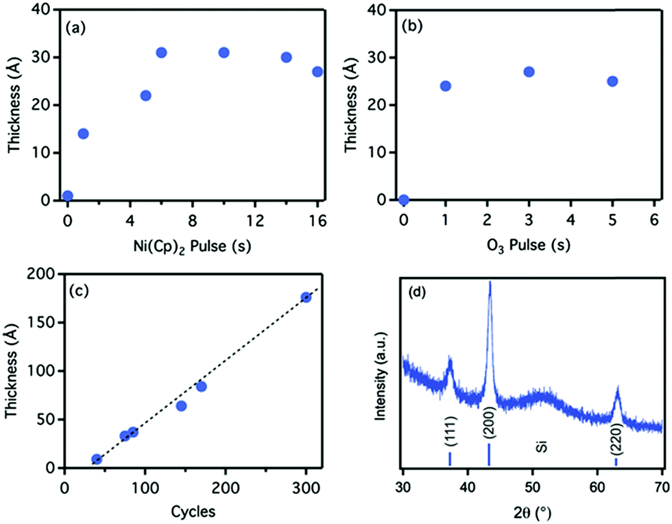 | ||
| Fig. 3 Self-limiting characteristics NiO ALD using Ni(Cp)2/O3 chemistry: saturation curves of thickness versus (a) Ni(Cp)2 pulse length and (b) O3 pulse length. The film thickness was measured after 75 cycles. (c) Growth curve for the Ni(Cp)2/O3 ALD in saturating regime. (d) XRD pattern of NiO thin film grown by ALD at 275 °C; the indexed peaks represent the FCC crystalline structure of NiO. (Reprinted with permission from ref. 29. Copyright 2015 John Wiley & Sons, Inc.) | ||
The deposition temperature can be significantly lowered by replacing O2 with O3. When the latter is used α-Fe2O3 can be obtained without any further treatment at temperatures as low as 200 °C.51 Even lower deposition temperatures (i.e., 120 °C) were demonstrated by Riha et al.52 In their work, they have also shown how to control crystalline phase of thin-film iron oxides by using a novel iron precursor, bis(2,4-methylpentadienyl)iron in combination with either ozone or H2O2. Using ozone would result in α-Fe2O3, whereas the use of H2O2 would allow the formation of Fe3O4. Both processes exhibited self-limiting chemistry and deposition rates of 0.06 nm per cycle. Other Fe-precursors such as bis(N,N′-di-t-butylacetamidinato)iron(II) (FeAMD)53 and FeCl354 have also been used for the deposition of Fe2O3 at moderate temperatures (200–350 °C). Nevertheless, such processes require a post-deposition annealing step (at 500 °C) to obtain single-phase α-Fe2O3.
2.2. ALD of metal nitrides
Similarly to ALD of metal oxides, ALD of metal nitrides such as TiN,55,56 TaN and Ta3N5,57,58 WN,59,60 and AlN61,62 has enjoyed a considerable development over the past few decades. ALD of metal nitrides has been widely applied in various fields, including microelectronics, optics, photonics, catalysis, and energy conversion and storage. Recently, considerable effort has been devoted to the development of silicon nitride Si3N4,63–65 hexagonal boron nitride,66,67 and gallium nitride,68–70 owing to their promising applications in semiconductor technology.2.3. ALD of metals
 | ||
| Fig. 4 TEM images of (a) highly dispersed Cu NPs on SiO2 grown by ALD, (b) commercial Cu/ZnO/Al2O3 catalysts (Sud-Chemie Catalysts, Inc.); and the Cu/SiO2 catalysts synthesized by impregnation method with different loadings: (c) 10.3 wt% and (d) 2.5 wt%. (Reprinted with permission from ref. 89. Copyright 2009 Elsevier.) | ||
 | ||
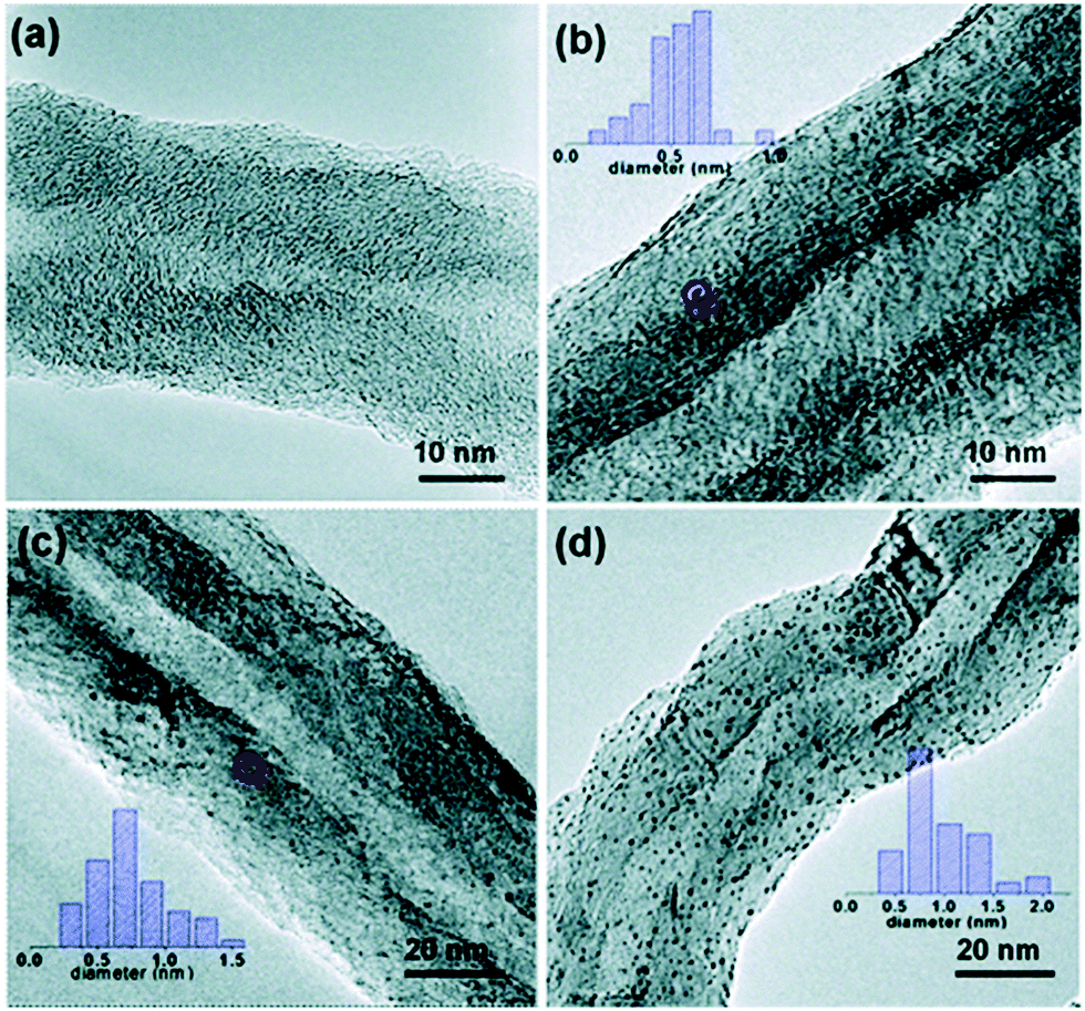
| Fig. 5 TEM images of Ni nanoparticles deposited on CNTs by ALD for (a) 50, (b) 100, (c) 200 and (d) 400 cycles, followed by hydrogen treatment. (e)–(h) Show TEM images at higher magnification. The insets in (e) and (f) show the SAED pattern and HRTEM image, respectively. (Reprinted with permission from ref. 109. Copyright 2016 Royal Society of Chemistry.) | ||
 | ||
| Fig. 6 (a) Schematic illustration of single-atom Pd/graphene catalyst synthesis via a process of anchor sites creation and selection and Pd ALD on pristine graphene. HAADF-STEM images of Pd/graphene at low (b and c) and high (d) magnifications. Atomically dispersed Pd atoms in image (d) are highlighted by the white circles. (Reprinted with permission from ref. 142. Copyright 2015 American Chemical Society.) | ||
 | ||
| Fig. 7 SEM images of ALD-grown Ag nanoparticles as a function of Ag dosing time, (a) 1 s, (b) 2 s, (c) 4 s, and (d) 6 s for 500 ALD cycles; (e–h) the corresponding particle size distributions. (Reprinted with permission from ref. 164. Copyright 2016 Elsevier.) | ||
2.4. ALD of metal sulfides
Although the most well established ALD processes are ALD of metal oxides, especially Al2O3 and HfO2 due to their applications in semiconductor technology, the Finnish inception of ALD was marked by ALD of a metal sulfide, namely, ZnS, by Suntola in 1970s.169 Since then, ALD processes for a number of sulfide-based materials have been developed, including CaS (1987), BaS (1987), SrS (1987), CdS (1988), PbS (1990), In2S3 (1994), CuxS (2001), WS2 (2004), TiS2 (2007), Sb2S3 (2009), SnS (2010), GaSx (2013), GeS (2014), MoS2 (2014), and Li2S (2014), as presented in the recent review paper by Dasgupta et al.170 However, ALD of metal sulfides has so far enjoyed a somewhat limited implementation in practical applications due to the use of H2S as the exclusive source of S in most processes. In fact, the use of H2S introduces severe limitations in terms of process compatibility due to its elevated toxicity, flammability and corrosivity.171 Nonetheless, the advantages brought about by ALD in terms of controllability coupled with the attractive properties of metal sulfide are fuelling the application of metal-sulfides ALD in photovoltaics, energy storage, and photonic applications. In particular, ALD of MoS2,172–176 WS2,177 PbS,178,179 and Li2S180 have gained increasing attention over the past few years. While MoS2 and WS2 (i.e., metal dichalcogenides) are more attractive in 2-dimensional form due to their exotic and tunable properties (see ALD of 2D transition metal dichalcogenides), the current research on ALD of thin films of Li2S and PbS mainly focuses on potential applications in Li-ion batteries.21,170,180 Recently, Sargent's group has further developed ALD of PbS to grow CH3NH3PbI3 (MAPbI3) perovskite thin films.181 In their work a PbS layer with a desired thickness was grown by ALD using Pb(tmhd)2 and H2S as precursors. The ALD-grown PbS layer was then exposed to iodine gas (I2(g)) to convert PbS to PbI2, which was in turn converted to MAPbI3 perovskite. While not being a pure ALD process, this approach provides an alternative route to grow high quality perovskite materials while retaining the advantages inherent to ALD such as controllability, uniformity, and conformality. As such this process enables the incorporation of perovskites into complex nanostructured devices.2.5. ALD of metal fluorides
Metal fluorides are excellent materials for optical coatings thanks to their wide bandgap (i.e., above 10 eV) and low refractive index, which translate into high transmission to wavelengths ranging from deep ultraviolet to infrared.182 ALD of thin films of metal fluorides, such as CaF2, SrF2 and ZnF2, has been carried out since the early 1990s.183 Nevertheless, the use of HF as the source of fluorine has hindered the development of the process due to its hazardous and corrosive nature. The development of precursors not requiring HF as co-reactant, such as TiF4,184 TaF5,185 and hexafuoroacetylacetone (hfac),186 has revived the interest in ALD of metal fluorides such as MgF2,184–186 LaF3,185 YF3,187 and AlF3.188 Another driving force for the development of ALD of metal fluorides lies in their promising application in passivation coatings for Li-ion battery. As a rule, metal oxides are widely used in several applications due to their high thermal and electrochemical stability. Li-ion batteries, being an inherently HF-rich environment, constitute an exception to the rule in that metal oxides readily degrade due to fluorination upon exposure to HF.186,189 From this perspective, metal fluorides represent ideal materials for passivation coatings of Li-ion batteries electrodes. Several studies suggest that an ultrathin film of metal fluorides such as AlF3,190,191 MgF2,186 and AlWxFy192 can enhance the stability of lithium-ion batteries against electrochemical cycling. The ALD-grown layer not only shields the electrode from the corrosive environment of the electrolyte (i.e., HF),186,190,193 but can also enhance its electrochemical performance. Sun et al. found that a layer of AlF3 grown by ALD on Li-enriched nickel–manganese oxide electrodes could induce leaching of Li, thus causing a phase change, which in turn resulted in improved the electrochemical performance of the electrodes.191 Such promising applications of ALD-grown films of metal fluorides have recently sparked a considerable interest in ALD of metal fluorides.194–1972.6. ALD of multicomponent materials
One of the greatest advantages of ALD is the capability of depositing multicomponent materials while controlling the composition to an extent hardly possible with any other synthesis routes. ALD of multicomponent materials can be achieved by combining different ALD chemistries in a sequential fashion. By doing so, the composition can be controlled by varying the relative number of cycles of each ALD process in the deposition sequence. Furthermore, the degree of intermixing of the components deposited via the different ALD processes can be further tuned by adding an annealing step.198An attractive application of ALD of multicomponent materials is the deposition of core–shell NPs. In particular, considerable effort has been devoted to ALD of core–shell NPs of noble metals pairs such as Pd/Pt,133,199,200 Ru/Pt,201 Au/Pt,202 and Pt/Pd.133,199 ALD of core–shell NPs relies on selective deposition. In particular, once the core material has been deposited on a substrate in the form of NPs, the subsequent ALD of the shell material should take place exclusively on pre-existing NPs. It follows that the choice of the underlying substrate, precursors, and experimental conditions such as temperature and pressure is crucial. For example, Weber et al. demonstrated the growth of Pd/Pt and Pt/Pd core–shell NPs.133 For the case of Pd/Pt, Pd NPs were first deposited on Al2O3 by plasma-enhanced ALD at 100 °C using Pd(hfac)2 and H2 plasma. The Pt was selectively grown on the Pd NPs by exploiting the fact that low O2 partial pressures hinder the growth on Al2O3 while retaining growth on Pd. In contrast, for the Pt/Pd case, high O2 partial pressures were employed to initiate the Pt nucleation on the Al2O3 surface. The Pd shell was then deposited by thermal ALD using H2 as reducing agent at 100 °C. The use of low temperature thermal ALD of Pd as opposed to plasma ALD prevented the undesired formation of metallic NPs. Lu et al. demonstrated ALD of Pt/Pd and Pd/Pt core–shell NPs using a different approach (Fig. 8).199 Instead of varying temperature and partial pressure, they relied on different precursor chemistries. The Pd(hfac)2/HCHO system was employed when Pd was the material of choice for the core, while the Pd(hfac)2/H2 system was used to grow Pd shells. In fact, the use of H2 as the co-reactant can suppress the nucleation of Pd on oxide surfaces, while retaining growth on metal surfaces. On the other hand, selective growth of Pt was achieved by using MeCpPtMe3 in conjunction with O3 to deposit Pt NPs on the substrate, and O2 to grow Pt shells. The work also demonstrated the ability to grow bimetallic PdPt alloys by alternating the ALD processes originally developed for the deposition of the individual metals. This approach can also be used to fabricate other bimetallic compounds such as CuPt,203 and IrPt.204 However, ALD of nanocomposites requires a certain degree of compatibility between surface chemistries and, crucially, a common deposition temperature.
 | ||
| Fig. 8 Structures of ALD bimetallic nanoparticles. Representative aberration-corrected HAADF-STEM images and corresponding EDS line profiles of (a) 5 (cycles) Pd-core 15 (cycles) Pt-shell, (b) 12Pt-core 20Pd-rich-shell, (c) 12Pt–Pd alloy and (d) 1Pt-core 35Ru-rich-shell bimetallic nanoparticles on spherical alumina support. (Reprinted with permission from ref. 199. Copyright 2014 Macmillan Publishers Limited.) | ||
Recently, ALD of ternary materials such as LixAlyS,205 BiFeO3,206 Ge2Sb2Te5,207 and of materials with higher number of components such as LiFePO4,208 LiPON,209 and (La,Sr)CoO3−δ210 have been reported. Cao et al. obtained LixAlyS by combining ALD of Li2S, based on lithium tert-butoxide and H2S, with ALD of Al2S3, based on tris(dimethylamido) aluminium(III) and H2S.200 In doing so, the film composition was precisely controlled by varying the relative ratio of Li2S and Al2S3 ALD cycles. Eom et al. combined three ALD processes, namely, Sb(OC2H5)3/[(CH3)3Si]2Te, Sb(OC2H5)3/[(CH3)3Si]3Sb, and Ge(OC2H5)4/[(CH3)3Si]2Te to obtain Ge2Sb2Te5 at a temperature as low as 70 °C.207 A triple ALD process was also employed to deposit LiFePO4 for high-performance cathodes for Li-ion batteries.208 Remarkably, ALD of quaternary compounds such as Cu2ZnSnS4 and (La1−xSrx)CoO1−δ has also been demonstrated.210,211 These recently developed ALD processes exemplify the potential of ALD in the synthesis of novel materials with tuneable properties.
2.7. ALD of 2D transition metal dichalcogenides
Unlike graphene, which is intrinsically a semimetal, 2D materials based on metal dichalcogenides (MX2, with M a transition metal and X a chalcogen) can exhibit insulating, semiconducting, semimetallic, or metallic properties depending on the metal/chalcogen pair. As a result, MX2 2D materials have promising applications in various fields such as nanoelectronics, catalysis, and energy generation and storage. In addition, due to the quantum confinement, MX2 monolayers exhibit electronic properties that are significantly different from those of their bulk counterparts. For instance, their bandgap switches from indirect to direct when the thickness of the material approaches one monolayer. This behaviour is especially relevant for nanoelectronics and optics.212,213 It follows that the ability to control the growth of MX2 is crucial to its implementation in practical applications. | ||
| Fig. 9 AFM images and height profiles of (a) tri-, (b) bi- and (c) mono-layers of MoS2 transferred onto a SiO2 substrate (scale bar = 0.5 μm). (d) Raman spectra and (e) photoluminescence spectra of tri-, bi- and mono-layer MoS2 on SiO2. (Reprinted with permission from ref. 176. Copyright 2016, Rights managed by Nature Publishing Group.) | ||
ALD performed at 100 °C yielded amorphous MoS2 films with high conductivity and excellent catalytic activity towards hydrogen evolution reaction (HER).174,175 Highly crystalline MoS2 thin films could be obtained by means of a post-deposition annealing step carried out at relatively high temperatures (i.e., 900 °C). Recently, the plasma-enhanced ALD of highly crystalline MoS2 films has been demonstrated on a wafer-scale SiO2 surface. Such approach provides a viable route for the deposition of high quality MoS2 layers for various applications.214
While 2D WS2 finds potential applications in Li-ion batteries, its selenide counterpart, namely, WSe2 has promising applications in field effect devices as a p-type semiconductor, owing to its excellent hole-mobility.218,219 Highly crystalline 2D WSe2 can be obtained via several routes such as exfoliation,220 selenization of WO3,221 and CVD.217,222 Analogously to the case of WS2, these methods can only provide high quality materials on small scales. Most recently, Park et al. have employed ALD to grow highly uniform, large-area WSe2 layers using WCl6 and diethyl selenide (DESe) as the precursors. In doing so, they demonstrated the ability to control the number of layers down to one single layer.223 Interestingly, the authors reported that the number of layers does not increase linearly with the number of cycles. Instead, the number of layers saturates after a critical number of cycles, depending on the growth temperature (i.e., 800, 700 and 600 °C correspond to 1, 3 and 5 monolayers, respectively). Such temperature dependence was also observed in ALD of MoS2 as reported by Kim et al.176 In addition, in this ALD process, H2 gas is introduced along with DESe to facilitate the reduction of WCl6 and the removal of chlorine by-products. The additional use of H2, in the form of plasma, was also applied in ALD of WS2 as reported by Delabie et al.177 Besides the enhancement in the reduction of the halide precursors, H2 plays an important roles in preventing the undesired oxidation of the surface.
2.8. ALD of MOFs
The growth of MOFs mainly relies on traditional solvothermal methods that require harsh processing conditions such as high temperature and pressure, which usually translate into limited throughputs, thus limiting the implementation of MOFs in practical application.224–226 In an attempt to circumvent such limitations, ALD has recently been applied to synthesis of MOFs. For example, Ahvenniemi et al. obtained highly crystalline copper(II)terephthalate (Cu-TPA) MOF thin films on silicon substrates by using and ALD scheme based on Cu(thd)2 and terephthalic acid.227 This work demonstrated that the properties of Cu-TPA MOFs (e.g., crystallinity, density, and roughness) are highly sensitive to the deposition temperature (Fig. 10). Crystalline Cu-TPA MOF thin films were obtained in a quite narrow temperature range (180–190 °C). The gas-storage capability of the ALD synthesized MOFs was tested via water absorption. | ||
| Fig. 10 Top: X-ray diffraction patterns recorded for as-deposited Cu-TPA films fabricated at different temperatures. Bottom: Patterns for the film as-deposited at 180 °C, then stored in open air for 26 days and finally annealed at different temperatures from 85 to 260 °C. (Reprinted with permission from ref. 227. Copyright 2016 Royal Society of Chemistry.) | ||
Recently, Parsons' group has demonstrated that the use of ALD-grown metal oxides such as TiO2, Al2O3, and ZnO can enhance the growth rate of MOFs, and, in particular, enable their synthesis at room temperature. The enhanced growth rates were obtained by exploiting the capability of ALD to tune the substrate wettability, surface roughness, and isoelectric point.224,228 The use of ALD can thus provide a tool for studying the influence of the substrate properties on the nucleation and growth of MOFs.228
2.9. Molecular layer deposition
MLD extends the use of self-limiting chemistry, and thus the advantages of ALD, to the deposition of thin films of organic and hybrid organic–inorganic polymeric materials.1 It is worth mentioning that some authors do not consider the deposition of hybrid films as an MLD process.8,229 Polymeric thin films find several applications in nonlinear optics and electroluminescent, electrochromic, and photochromic materials. However, as recently pointed out by Cameron and Ivanova,229 the application of MLD is limited by the instability of the most organic precursors and the resulting polymeric layers. For this reason, the deposition temperatures are usually low and the corresponding temperature window within which the GPC is constant is either very narrow or non-existent.229 MLD was first proposed by Yoshimura and co-workers in Japan,230 who used a dianhydride (pyromellitic dianhydride) and a diamine (2,4-diaminonitrobenzene or 4,4′-diaminodiphenyl ether) to grow thin films. They measured the thickness using a quartz oscillator thickness monitor, and demonstrated self-limiting growth. It should be noted that determining the thickness of organic films is more challenging than that of its inorganic counterparts, since e.g. transmission electron microscopy is not easy to apply. They demonstrated the scheme up to 15 cycles (∼10 nm film). In the years after, other precursor types such a diacidic, dichlorides, and diols have also been used.8 In 2007, Nilsen et al.231 and George et al.232 proposed the first schemes for hybrid MLD: they produced a layer that is not fully organic, but also contains metal atoms. This approach introduces even more degrees of freedom. By mixing the precursors for oxide growth using ALD with those used for MLD, one can also tune the degree of incorporation of the organic component in the films.233 An additional difference with fully organic MLD is that the incorporation of metal atoms typically leads to 3D networks. In fully organic MLD, normally linear polymer chains are formed. Such chains are likely to tilt, giving growth that is not perpendicular to the surface. Tilted and/or bulky chains can cause steric hindrance. Moreover, the precursor molecules may bend and react twice with the surface, lowering the number of reactive sites, and leading to a lower growth rate;8 see Fig. 11. | ||
| Fig. 11 In the ideal situation, the MLD precursor reacts with one surface site and remains straight (left). However, it can also react twice with the surface (middle) of tilt (right). (Reprinted with permission from ref. 8. Copyright 2014 Sundberg and Karppinen; licensee Beilstein-Institut.) | ||
George et al.232 grew the alucone poly(aluminum ethylene glycol) using trimethylaluminum and ethylene glycol. Dameron et al.234 report that the GPC is highly dependent on temperature: from 0.4 nm per cycle at 85 °C to 0.04 nm per cycle at 175 °C. Later on, other metalcones such as zincone,235 titanicone,236 and zircone237 were made by MLD. Also for these compounds it is typically observed that the GPC drops quickly with increasing temperature.
While most MLD schemes are the AB-type (sequence A–B–A–B–…), an ABC-type was first proposed by Yoon et al.238 (Fig. 12). They used trimethylaluminum, ethanolamine, and maleic anhydride. Using this chemical scheme, they obtained a higher GPC compared to AB-type (2.4 nm per cycle at 90 °C to 0.4 nm per cycle at 170 °C). The probable reason is that one of the major problems with AB binary reaction sequences is avoided: the “double” reactions between the homobifunctional reactant and neighbouring surface species.238 ABC-type schemes expand the number of possible organic reactants, and give the opportunity to incorporate particular functionalities into the film.
 | ||
| Fig. 12 Schematic of three-step reaction sequence for ABC alucone growth using (A) trimethylaluminum (TMA), (B) ethanolamine (EA), and (C) maleic anhydride (MA). (Reprinted with permission from ref. 238. Copyright 2009 American Chemical Society.) | ||
Adamczyk et al.239 were the first to apply MLD to particles instead of to flat substrates. They deposited poly(p-phenylene terephthalamide) (PPTA) thin films on high-surface area silica nanopowders. Their reason to use particles as the substrate is that it improved the signal-to-noise ratio for transmission FTIR. Liang et al.240 used a fluidized bed to coat particles by MLD: they deposited alucone on silica and titania particles. A fluidized bed is attractive for coating larger batches of particles, given its good mixing characteristics. The growth rate varied from 0.5 nm per cycle at 100 °C to 0.35 nm per cycle at 160 °C, which is much higher than the growth rate of MLD films grown on small amounts of particles at a small scale. The higher film growth rate could be caused by localized CVD, since ethylene glycol is sticky and TMA can adsorb into the polymer films. Vasudevan et al.241 were the first to apply MLD at atmospheric pressure. They coated fluidized enzyme particles using malonyl chloride and 1,2-butanediol. Especially when carrying out MLD in a fluidized bed working at atmospheric pressure is attractive, since it is much easier to keep particles fluidized with an inert gas stream at atmospheric pressure.
Metalcones are typically not stable when exposed to water or high temperatures. While this might be a disadvantage for some applications, they could be utilized to produce porous materials. Liang et al.240 showed that porous structures can be obtained by either mild water etching at room temperature or calcination in air at elevated temperatures. In this way, they turned an alucone layer (50 cycles) on silica nanoparticles into a membrane with ∼0.6 nm micropores and ∼4 nm mesopores. The method used (soaking versus calcination) and the specific parameter settings gave some differences, but to a certain extent, the obtained membranes were comparable. Such membranes are attractive for e.g. use in catalysis and drug delivery. Seghete et al.242 grew alucone to make sacrificial layers: in this way gaps between features in MEMS and NEMS devices can be created (e.g., for charge separation or thermal insulation). The alucone was deposited via both an AB and an ABC mechanism, and tested with several wet etching methods which demonstrated MLD as a versatile method to obtain sacrificial layers.
Räupke et al.243 applied MLD for making luminescent materials, that could find application in sensors, photocatalysts and solar cells. Monolayers of Alq3 (tris(8-hydroxyquinolinato)aluminium) were grown on silica aerogel disks by MLD using TMA and 8-hydroxyquinoline (8-HQ). Compared to conventional physical deposition methods which only coat the aerogel surface, MLD provides the ability to coat porous structures without limitations of shadowing, and allows for deeper penetration of the coating into the aero gel disc. Kim et al.244 used MLD to make platinum-free cathodes for dye-sensitized solar cells. Poly(3,4-ethylene-dioxythiophene) (PEDOT) thin films were deposited on mesoporous ITO substrate by oxidative MLD. The method provided a high surface area substrate with high conductivity and connectivity of PEDOT within the cathode, enhancing efficient electron transport and catalytic activity toward the reduction of I3−.
Tanskanen and Karppinen245 deposited inorganic–organic hybrid thin films of the (–Fe–O–C6H4–O–) n type using cyclopentadienyl iron dicarbonyl dimer (Cp2Fe(CO)4) and hydroxyquinone as precursors, resulting in a growth rate of 0.37 nm per cycle at 180 °C. Such materials could find application in flexible electronics. Recently, Nisula and Karppinen246 used MLD to make Li-ion battery anodes. Crystalline lithium terephthalate (Li2C8H4O4) thin films were deposited using Li(thd) and terephthalic acid in the temperature range of 200–280 °C. Growth rate drops rapidly with increasing temperature. The authors reported that the deposited Li-terephthalate films provide excellent rate capability without the requirement of conductive additives.
Summarizing, the recent developments of MLD have offered a wealth of opportunities to deposit organic and hybrid films. Although the number of publications is still limited, we expect this field to rapidly grow in the coming years.
3. Substrates
In principle, ALD can be used to deposit materials on virtually any substrate. Historically, ALD has been mostly applied to flat substrates, as its development was fuelled by its application in semiconductor technology. To date, several ALD processes have extended the application of ALD to substrates of different nature and geometry such as such as particles, carbon nanotubes, graphene, and porous media.3.1. Particles
Particles are omnipresent in industrial applications. For instance, they find application in catalysis, pigments, energy storage and generation, pharmaceuticals, and lighting devices. The properties of particles are strongly dependent on their surface chemistry. Therefore, by engineering their surfaces, one can adjust the material properties to meet the requirements of the target application. From this perspective, given its ability to tune surfaces at the sub-nanometre level, ALD is an ideal technique for imparting functionality to particles, and in particular, nanoparticles and micron-sized particles.119,247 As King et al.248 wrote an excellent review on ALD/MLD on particles, we will keep this section brief. ALD on particles finds application in, for example, the synthesis of enhanced catalysts, encapsulation, and surface passivation. For example, ALD of NPs of metals such as Pt and Ni has proven to be a viable route to enhance the photocatalytic activity of TiO2 nanopowders in a highly controlled fashion.119,120 Moreover, TiO2 NPs are also widely used as white pigment in paints, thanks to their high brightness, refractive index, and photostability. However, TiO2 NPs can promote the decomposition of the organic compounds present in the paint upon exposure to sunlight, thus reducing its lifetime. To circumvent this inconvenience, TiO2 NPs can be coated by ALD with an inert and optically transparent thin layer in order to suppress their catalytic activity while retaining the white colour.249 Finally, ALD on particles has been demonstrated for the deposition of various materials such as Pt,117,119,120 Pd,138,139 Ni,105 BN and SiN,248 NiO,31 Fe2O3,248 SiO2250 and Al2O3.251 MLD has also been applied to grow organic layers on nanoparticles.248,249,252 Since ALD on particles is best carried out in dedicated reactors, we will pay some more attention to this topic in Section 6: Reactors.3.2. 1D materials
ALD of uniform V2O3 thin films on porous CNTs was demonstrated by Boukhalfa et al.257 The ALD-grown V2O3 layer on the MWCNTs resulted in a significant improvement of their stability towards cycling as well as in an enhancement of the electrochemical performance and specific capacitance of the capacitors. Furthermore, the use of ALD, thanks to its atomic-level control over the film thickness, enabled the investigation of the influence of the coating thickness on the performance of the V2O3/CNT cathodes in supercapacitors. Conformal thin films of another form of vanadium oxide, V2O4, have also been deposited on CNTs.258 Interestingly, a p–n heterojunction is formed at the interface of the n-type V2O3 layer and the p-type CNT support, which was used as an active component in gas-sensing devices.258
The deposition temperature was found to have strong influence on the morphology and crystallinity of ALD TiO2 on CNTs based on Ti(OCH(CH3)2)4 and H2O.254,255 A conformal and homogeneous TiO2 film was obtained at a temperature of 60 °C. The morphology shifted to a “pearl necklace” structure at a deposition temperature of 120 °C, and a deposition temperature of 220 °C resulted in an extremely rough TiO2 surface. At 60 °C, the film was amorphous, whereas at 220 °C the layer was almost entirely crystalline (anatase). In addition, conformal TiO2 layers with anatase phase could also be obtained on non-functionalized CNTs in a temperature-step ALD, in which the nucleation was performed at low temperature (i.e., 60 °C), followed by an increase to 220 °C during the growth stage.
In contrast to TiO2 ALD, ALD of NiO resulted in discrete NPs when carried out on CNTs. Such CNTs-supported NiO NPs have proven to be an excellent catalyst in methanol oxidation reactions.259 Importantly, the size of NiO NPs can be controlled by simply varying the number of ALD cycles. This feature enabled the study of the size- and mass-dependency of the electrochemical activity of the redox reaction of NiO in KOH solution.259 The NiO NPs/CNT thus deposited can be reduced in H2 to form metallic Ni/CNTs as presented above (see Fig. 5). Highly dispersed Ni NPs/CNTs could also be directly grown by ALD (i.e., without a reduction step).260
Among the metals that have been deposited on CNTs by ALD, Pt/CNTs has attracted most attention due to its potential application in catalysis and fuel cells.122,203,261,262 Liu et al. deposited Pt NPs on CNTs for applications in proton-exchange membrane fuel cells; the ALD-grown Pt/CNTs exhibited higher Pt utilization efficiency compared to commercial E-TEK electrodes.122 Remarkably, Li et al. have recently demonstrated that uniform and highly dispersed sub-nanometre clusters of Pt on CNTs can be obtained (Fig. 13).261 In this case, a surface pretreatment in HNO3 solution was applied prior to ALD to remove impurities and to create an oxygen terminated surface that is necessary for the uniform nucleation of Pt. The ability to control the particle size at sub-nanometre level enabled the study of the influence of the particle size on the catalytic performance of the Pt/CNTs in styrene hydrogenation. The turnover frequency (TOF) was found to be a strong function of the Pt particle size. In particular, an average Pt particle size around 0.5–0.7 nm exhibited the highest TOF value.261
 | ||
| Fig. 13 TEM images of the Pt/CNTs catalysts prepared by ALD at 300 °C using MeCpPtMe3 and O3 for (a) 2 cycles, (b) 5 cycles (c) 8 cycles and (d) 10 cycles. (Reprinted with permission from ref. 261. Copyright 2016 Royal Society of Chemistry.) | ||
MLD has also recently been applied for coating CNTs with polymers.263,264 Brown et al. coated CNTs with different metalcones, including alucone (using TMA/glycerol and TMA/ethylene glycol), titanicone (using TiCl4/glycerol), and zincone (using diethyl zinc/glycerol).264 The coatings significantly improved the mechanical properties of the CNTs. Uniform and conformal coatings of polyurea films on CNTs by MLD have recently been reported by Chen et al.263 The MLD was carried out using 1,4-phenylene diisocyanate (PDIC) and ethylenediamine (ED) at a typical temperature of 65 °C. The thickness of the polyurea could be controlled by varying the number of MLD cycles. The polyurea layers allowed for better dispersion of the CNTs in highly polar solvents and improved the compatibility between the CNTs and the polyurethane matrix used for fabricating a CNTs-based composite. In particular, the coated layer significantly increased the tensile strength and modulus of the CNTs-based composite.
The ability to control the size deposited NPs makes ALD an excellent technique for the fabrication of quantum dots (QDs), as their properties are inherently size-dependent.271 Dasgupta et al.179 demonstrated ALD of PbS quantum dots on Si NW. The size of the QDs could be tailored by varying the number of ALD cycles and via a post-deposition heat treatment. This concept can be applied for the fabrication and integration of QDs in three-dimensional nanostructured devices. The combination of noble metal NPs (e.g., Pd, Pt) and silicon NWs has shown excellent catalytic performance in several reactions.272,273 This is due to the facile electron transfer between the NW and the metal NPs. Using ALD, Dai et al.266 demonstrated that uniformly dispersed single-crystalline Pt NPs can be deposited on Si-NWs at a temperature of 250 °C (Fig. 14). The coupling of Si-NWs with the ALD-grown Pt NPs resulted in a significant enhancement in the activity towards the compared to the bare Si-NWs. This enhancement has also been reported in parallel work by Dasgupta et al.267
 | ||
| Fig. 14 Electron micrographs of SiNWs decorated with ALD Pt. (a) Cross-sectional scanning electron micrograph (SEM) showing no obvious catalyst aggregation. (b) Low-magnification transmission electron micrograph (TEM) showing the distribution and uniformity of ALD Pt. (c) High-resolution TEM showing the crystalline quality of Pt particles grown on the SiNW surface by ALD. The existence of amorphous SiO2 is indicated by an arrow. (Reprinted with permission from ref. 253. Copyright 2015 John Wiley & Sons, Inc.) | ||
3.3. Graphene
For more than a decade since its discovery, graphene has been considered as one of the key materials of future electronics due to its unique electronic properties.274 Much effort has been devoted to the development of graphene-based field effect transistors.275,276 ALD of high-k dielectric gate materials (i.e., Al2O3 and HfO2) on graphene has therefore attracted enormous attention in the ALD community.277–280 However, as the inert nature of graphene inhibits the chemisorption of ALD precursors, ALD on bare graphene usually results in non-uniform coatings. To overcome this problem, a surface pretreatment step is usually applied prior to the deposition. Lee et al.277 demonstrated ALD of Al2O3 on graphene using TMA and either H2O or O3 as precursors. Without surface pretreatment, the growth of Al2O3 only occurred on the edges of the graphene for the TMA/H2O process, and extended partially to the basal planes for the TMA/O3 process. On the other hand, when an ozone treatment step was applied prior to ALD, a uniform and conformal growth of Al2O3 was obtained. This was ascribed to the fact that the ozone pretreament resulted in the formation of epoxide (or ethers) and carbonyl functional groups, which acted as nucleation sites for the Al2O3 ALD. To obtain uniform nucleation and growth with the TMA/H2O process, Young et al.281 applied a pretreatment procedure consisting of five NO2/TMA cycles.Graphene-supported nanoparticles (NPs) are emerging as a novel class of high-performance catalysts. The use of graphene as a support for NPs, and catalytic material in general, boasts several advantages. For instance, the high chemical, thermal and mechanical stability of graphene makes it an ideal support for durable catalysts.282,283 Its high specific surface area, coupled with the high surface sites-to-volume ratio of NPs, enables high active site dispersion. Moreover, graphene not only acts as a passive support, but also can enhance the catalytic activity of the supported NPs owing to its high electron mobility, which can facilitate the electron transfer during chemical reactions.282,283 Hence, the coupling of NPs and graphene opens up new avenues for meeting the incessant demand for high performance catalysts. Nanoparticles of several metal oxides and metals have been deposited on graphene by ALD, such as TiO2,284,285 ZnO,286 SnO2,287 Pt,6,124,288 and Pd.142,143 Sun et al. applied the MeCpPtMe3/O2 ALD process to deposit single atoms and sub-nanometre Pt NPs on graphene at a temperature of 250 °C (Fig. 15).124 The morphology, size, density and loading of Pt could be precisely controlled by adjusting the number of cycles. The obtained catalysts exhibited significantly higher catalytic activity towards methanol oxidation compared to commercial Pt/C catalysts.
 | ||
| Fig. 15 HAADF-STEM images of Pt/GNS samples. (a–c) Present the results with 50, 100, and 150 ALD cycles, respectively, and (a′–c′) show the corresponding magnified images. Inset in each figure show the corresponding histogram of Pt on GNS. (Reprinted with permission from ref. 124. Copyright 2013 Macmillan Publishers Limited.) | ||
ALD of atomically dispersed Pd on graphene has been also realized by Yan et al.,142 as shown in Fig. 6. The single-atom Pd/graphene thus fabricated showed unprecedented catalytic performance towards selective hydrogenation of 1,3-butadiene, while exhibiting a good stability after a long reaction times (i.e., up to 100 h). In order to obtain uniformly dispersed Pd, a solution-based method was used to preoxidize the graphene. Recently, we demonstrated a 100% solvent-free, controllable and scalable process for producing bulk quantities of Pd/graphene using atmospheric pressure ALD in a fluidized bed reactor.143 The nucleation and growth of Pd NPs on the inert graphene was enabled by applying an ozone pretreatment step. Interestingly, by controlling the pretreatment time, selective growth of Pt NPs on the edges of the graphene was achieved. This selective growth was also observed for ALD of Pt on untreated graphene by Kim et al.,6 in which Pt mainly deposited on at the graphene line defects. Such a selective growth showed great potential for sensing applications.6
A number of oxides have been successfully deposited on graphene, including TiO2,284,285,289 SnO2,287 and ZnO.286 The studies on these materials have revealed their excellent properties for applications in supercapacitors and Li-ion batteries. The ALD-grown TiO2 NPs on graphene powders created strong chemical bonding with the support that resulted in excellent electrical conductivity and stability compared to conventional deposition methods.284 As a supercapacitor material, TiO2/graphene exhibited superior electrochemical performances with good capacity retention at a high scan rate. Using the same ALD chemistry (TiCl4/H2O), thin films of TiO2 on graphene have also been realized by ALD. However, an Al2O3 adhesion layer was needed in order to obtain conformal films.285,289 The deposition at a relatively low temperature (i.e., 120 °C) resulted in amorphous TiO2 layers, which are suitable for electrode materials in Li-ion batteries and supercapacitors due to their high porosity and surface area.290
Very recently, MLD has been applied to the coating of graphene with aromatic polyimide (PI) films.291 This MLD process employed pyromellitic dianhydride (PMDA) and 4,4′-diaminodiphenyl ether (ODA) as precursors and was carried out at a relatively low temperature (i.e., 160 °C). An annealing step was then applied to the as-deposited materials to carbonize the PI layer. This resulted in the formation of a N-doped carbon layer on the graphene surface. This material exhibited remarkable capacitance performance as electrode material for supercapacitors. The application of MLD enables not only the deposition of uniform PI layers on the pristine surfaces, but also the homogenous dispersion of doped nitrogen atoms in the carbon layer, which has a strong influence on the performance of the supercapacitors.291
3.4. ALD on porous materials
Porous materials find application in several fields such as catalysis, separation, and energy storage. The properties and thus the potential application of a porous material depend on its internal structure (e.g., pore size) and surface chemistry. In that respect, ALD represents an ideal tool for tailoring both the structure and the functionality of porous materials. For instance, the excellent film conformality achievable by ALD coupled with its sub-nanometre control over the film thickness, can be exploited to tune pore sizes with unparalleled precision.22,292–294 This feature is particularly relevant to the fabrication of size-selective membranes and catalysts. ALD-grown thin films can also be used to enhance the structural stability of porous materials. Furthermore, ALD enables the fine-tuning of surface functionality of porous materials by enabling the deposition of controlled amounts of heteroatoms of various nature.22,295 As Detavernier et al.296 have already extensively illustrated how ALD can be used for tailoring nanoporous materials, we will now only briefly review a novel application of ALD that is ALD in metal organic frameworks (MOFs).4. Energy-enhanced ALD
The two most widely used ALD modes are thermal and plasma-enhanced ALD. The latter is also referred to as plasma-assisted ALD or radical-enhanced ALD. The use of these two ALD modes accounts for the deposition of all the materials that have been reported so far,7,20i.e., other modes have also been investigated, although not for depositing new materials. Thermal ALD is a purely surface-driven process, as deposition occurs exclusively via surface reactions. As a result, thermal ALD enables excellent conformality and thickness control irrespectively of the substrate geometry and reactor design. Furthermore, thermal ALD can be carried out in a wide range of pressures, ranging from high vacuum to atmospheric pressure.248,296,304 However, in thermal ALD the surface reactions are exclusively driven by thermal energy. For this reason, thermal ALD processes typically require relatively high temperatures (typically 150–350 °C), which might limit their applications. Furthermore, thermal ALD suffers from long incubation periods, from a few tens of cycles to more than hundred cycles, when carried out on substrates that lack suitable active sites.305 Such shortcomings can be addressed by using plasma-enhanced ALD (PEALD).306 In PEALD, the use of plasma during one of the reacting steps provides highly reactive species such as radicals that promote the growth in addition to the thermal budget from the substrate. As a result, PEALD is not subject to nucleation delays,307 and enables depositions at temperatures as low as room temperature.155,308 Furthermore, the use of plasma at low temperatures widens the range of substrates and precursors that can be used.63,309 Nevertheless, PEALD suffers from several limitations.306,310–313 In fact, plasma not only generates radicals that promote ALD growth, but can also activate undesired side-reactions. For example, in ALD on high-aspect-ratio structures and porous materials, radicals diffusing within the substrate might undergo surface recombination upon collision with the pore walls, thus creating spatial gradients in radical concentration, which can in turn result in deposition inhomogeneity.312,313 Furthermore, reactions between radicals within the plasma and surface species might lead to the incorporation of undesired impurities.Hot-wire ALD is a novel technique that has the potential to overcome the limitations of PEALD in terms of conformality and impurities inclusion, while retaining the advantages of an energy-enhanced method.78,79,314–316 This approach employs a filament that is heated up to a temperature above 1000 °C in order to dissociate reactant molecules, such as oxygen and hydrogen, into radicals (Fig. 16). By tuning the temperature of the filament, the concentration of the radicals can be controlled.317 This approach has been employed for ALD of several metals, such as W,78,79 Ni,316 and Co.314
 | ||
| Fig. 16 Schematic representation of the hot-wire apparatus for ALD. Gas molecules are dissociated into atoms and introduced to the reactor. In this design, the hot-wire is located outside of the reaction chamber. Therefore, the influence of the hot-wire on the chemical reaction on the substrate surface is negligible. Image courtesy of Tom Aarnink (University of Twente). | ||
Another form of energy-enhanced ALD that has gained increasing attention is photo-assisted ALD. As in PEALD and hot-wire ALD, photo-assisted ALD exploits the highly reactive nature of radicals/atoms to enhance the growth. In this case, the radicals are generated by photo-induced reactions promoted by exposure of the reactants to ultraviolet (UV) radiation.318,319 In fact, the interaction between reactant molecules (e.g., O2, H2O) and photons can result in the excitation and/or dissociation of the molecules. For example, for a water-based process radicals can form via the following reactions:319
| H2O + hν → H* + OH*, for λ = 175–190 nm |
| H2O + hν → H2 + O, for λ < 175 nm |
| O2 → O(3P) + O(3P), for λ = 185–240 nm |
| O2 → O(1D) + O(3P), for λ < 185 nm |
5. Processing conditions in ALD
ALD processing conditions and reactor designs can vary considerably depending on the nature of the substrate and the material to be deposited. However, the design rationale of an ALD process is typically dictated by the need for minimizing operating times, thus maximizing throughput, while retaining a self-limiting deposition. ALD surface reactions are active and self-limiting only within a certain region or “window” in the parameter space of temperature, time and pressure. Identifying such a region is therefore the first step towards the design of every ALD process. Historically, the “ALD window” was described solely in terms of temperature range, probably due to the fact that most deposition experiments were carried out at fixed exposures (pressure × time).2 Recently it has become clear that to fully understand the self-limiting nature of ALD growth one has to include time and pressure in the picture. In fact, ALD surface chemistry has often been depicted in terms of sequential chemisorption reactions, while reality is more complex. At every stage of the ALD process, several reactions take place simultaneously and at different rates, including those which are not self-terminating. It follows that whether the growth is dominated by ALD reactions (e.g., precursor chemisorption) or by undesired reactions (e.g., precursor decomposition and desorption, and etching reactions) depends on the relative magnitude of the reaction rates and the timescale of the experiment, or in other words on kinetics.324,325 Since, reactions rates are finite functions of the temperature and the partial pressure of reactants, one can in principle tune temperature, pressure and time so as to selectively suppress undesired reactions and “activate” the desired ALD reactions. Furthermore, if the substrate is heterogeneous, reaction rates on different part of the substrate will inherently have different temperature and pressure dependence. Such principle has been recently exploited to achieve area-selective ALD.326 Hence, in ALD the choice of the process conditions is strongly tied to surface chemistry considerations. However, it must be noted that ultimately self-limiting deposition can only be achieved by solving two mass transfer problems, namely, the delivering of gaseous precursors to the substrate surface and the complete removal of reaction by-products and unreacted precursors after each reacting step. In the following paragraphs, we will illustrate in greater detail how temperature, time, and pressure can be chosen on account of their effect on surface chemistry and mass transfer. Emphasis will be placed on those effects that, despite being partially unexplored, could open up new avenues for the development of novel ALD processes.5.1. Temperature
The strong reliance of ALD on surface reactions, and thus activated processes, makes the temperature one of the most important parameters in every ALD process. As already mentioned, ALD has often been described in terms of the temperature range (ALD window) within which ALD reactions are both active and self-limiting. As such the ALD window is dictated by both the intrinsic properties of the precursors and the unique precursor–substrate chemistry. With regard to the latter, ALD growth can proceed only if the chemisorption reactions are fast and irreversible relatively to the time scale of the ALD experiment. For this reason, the ALD window is bounded at one end by low precursor reactivity at low temperatures, and at the other by the onset of desorption reactions at high temperatures.The precursor itself can disrupt the self-limiting behaviour, thus further narrowing the ALD region, both at low temperatures due to uncontrolled condensation and at high temperatures due to thermal decomposition (CVD-like reactions). Most ALD chemistries are based on sequential exposures of CVD precursors at low temperatures. However, this transposition is not always possible as the precursor chemisorption might not be active at temperatures below the decomposition temperature. For this reason, the advent of ALD has spurred the development of dedicated ALD precursors that can outperform CVD precursors in terms of volatility, reactivity, and thermal stability.1,2,7,100
Within the ALD window, the GPC can vary with the temperature. For example, this can be due to the fact that the temperature can change the nature and the number of active sites. In the trimethylaluminum/water process the GPC is known to be a decreasing function of the temperature.2,327 Such dependency has been ascribed to the temperature-dependent desorption of hydroxyl groups, which are considered the main active site for the chemisorption of trimethylaluminum.327 Another reason behind the temperature dependence of the GPC is the fact that, in each precursor exposure, several surface reactions take place at the same time and the dominant reactions, and thus the number and the nature of surface species that remain adsorbed in the timescale of the ALD experiment, can in principle vary with the temperature.2,324,325,328 Nevertheless, such variations are usually of the order of a fraction of a sub-monolayer, therefore when compared with CVD or wet-chemistry synthesis routes, ALD is virtually insensitive to the deposition temperature (within the ALD window).
In sum, the range within which the deposition temperature can be chosen is set by the ALD chemistry of choice. Once the range is defined, the optimal temperature depends on the nature of the substrate, the desired morphology, and energy consumption considerations. In most cases, it is desirable to choose the deposition temperature as close as possible to the lower end of the ALD window. ALD surface reactions lead to the deposition of atoms that are not arranged in the most thermodynamically stable form and the degree to which they approach it largely depends on the deposition temperature. For this reason, the lowest deposition temperature is chosen when the thermal budget has to be minimized in order to avoid interdiffusion between the ALD-grown material and the substrate.1 Furthermore, as a rule, low deposition temperatures usually translate into amorphous films, whereas high deposition temperatures promote the formation of crystalline films.7 Therefore, depending on the final application, one can tune the deposition temperature so as to obtain either an amorphous or a crystalline film. If conformality is the main concern, low deposition temperatures are again desirable, as ALD-grown amorphous films tend to have the better conformality and lower roughness than crystalline films.7,329,330 Moreover, when the affinity between substrate and ALD-grown material is such that island growth is the preferred growth regime: the surface density, the size and the morphology of the deposited islands or nanoclusters strongly depend on the temperature. Hence, if ALD is to be used for the deposition of size-selected NPs, the lowest temperature should be chosen in order to minimize NPs sintering and thus the undesired broadening of their size distribution. Finally, low deposition temperatures are also preferred when the substrate is heat-sensitive and/or energy consumption is a major concern.1
5.2. Pressure
The choice of the operating pressure in ALD processes is usually based on considerations on mass transfer and process scale-up rather than on surface chemistry. However, the pressure represents another handle for steering the surface chemistry towards the desired reaction path, which is up to now hardly exploited. For the sake of clarity, it is worth to emphasize the distinction between the absolute operating pressure and the partial pressure of precursors. At any given time, the absolute pressure in an ALD reactor is given by the sum of the partial pressures of the precursors, the reaction by-products, and the carrier gas, if present. ALD surface chemistry is mostly dependent on the partial pressure of precursors as it rests on adsorption reactions. However, in some instances, the partial pressure of the reaction by-products and the carrier gas can be expected to also affect the growth. For example, both reaction by-products and carrier gas molecules could mediate the precursor adsorption by competitive physisorption. Even though in most instances the carrier gas is not expected to participate directly in adsorption reactions, as it is usually an inert gas, it can still affect ALD growth by mediating the surface diffusion of adsorbed species via weak gas–solid interactions.331 In principle, high inert gas pressures can also thermodynamically stabilize adsorbates that would otherwise desorb at lower pressures. Furthermore, by-products formed upon adsorption can lead to subsequent etching reactions that can effectively change the nature and the density of surface active sites during both the reacting and the purge steps. This is especially the case for halogen-based precursors. That being said, the effect of pressure on ALD surface chemistry remains largely unexplored. This is mostly due to the fact that studying the effect of the pressure on the concentration of adsorbed species is extremely challenging as they both vary continuously during an ALD cycle. Several studies report the effect of the partial pressure of precursors on the GPC at a given exposure time.2,332 However, it must be noted that the reported partial pressure is hardly the one experienced by the surface of the substrate. In fact, since most ALD chemistries enjoy fast kinetics and precursors are usually not supplied in great excess, the precursor partial pressure inside the reaction chamber rapidly drops upon exposure, as the ALD surface reactions deplete precursor molecules. Even when the precursor is supplied in excess, the typically fast ALD surface reactions are likely to deplete the precursor molecules at a higher rate than diffusion would allow, thus resulting in a gradient in the partial pressure between the substrate surface and the bulk of the gas.332,333 As a result, most of the reported changes in GPC with the partial pressure have usually little to do with the actual ALD surface chemistry. Instead, they are mostly an empirical measure of the amount of precursor that has to be introduced in the reaction chamber to obtain saturation at a given exposure time and for a given reactor design.333,334 In recent years, this gap of knowledge has seen several researchers devoting considerable effort in the deconvolution of reactor dynamics and surface chemistry via both mathematical modelling and in situ measurements.333–339 Nonetheless, since most ALD reactions reach saturation on time scales of the order of milliseconds over wide ranges of precursor partial pressure, the lack of a detailed understanding of the ALD surface chemistry has not hampered the development and application of most ALD processes. On the other hand, the role of pressure is still particularly relevant to ALD processes that are based on inherently slow kinetics. For example, ALD of catalytic metals often relies on the combustion of organic ligands via exposure to an oxidizer.1,2,7 The rate of combustion of adsorbed carbonaceous material is known from heterogeneous catalysis to be strongly dependent on the partial pressure of the oxidizer and the nature of the underlying substrate. Mackus et al.326 recently achieved selective growth on alumina-supported platinum NPs by exploiting the fact that, below a certain oxygen partial pressure, combustion reactions are active on pre-existing Pt NPs and effectively suppressed on bare alumina, in the timescale of their ALD experiments. Finally, pressure is expected to have an important role in all the ALD processes that result in the deposition of NPs, as the latter form and grow via surface diffusion, which in turn is known to be strongly affected by the nature and the partial pressure of the chemical species present in the reactive environment.Most conventional ALD reactors operate at vacuum (<1 mbar). Low operating pressures are typically preferred as they facilitate the purge step and help mitigating the incorporation of impurities.1 However, since the cost and the complexity of vacuum equipment represent an obstacle to the scale-up of the process, great effort has been devoted to the development of atmospheric pressure ALD.1,119,332,339,340 Operating at atmospheric pressure, not only simplifies the reactor equipment, but also widens the range of precursor partial pressures that can be employed. This is especially relevant for ALD on high-surface-area substrates, which typically require large amounts of precursor for reaching surface saturation. In fact, given that the amount of precursor delivered to the reactor is proportional to the product of the precursor partial pressure and the exposure time, it follows that high precursor partial pressures are desirable if throughput is to be maximized.
5.3. Time
Despite the inherent dynamic nature of ALD, the current understanding of self-limiting deposition is mostly framed in thermodynamics rather than kinetics.341 In the classic picture of ALD, the surface species formed upon precursor chemisorption must be thermodynamically stable for the surface chemistry to be self-limiting. However, as recently pointed out by Pedersen,342 even when the adsorbed monolayer is not thermally stable, one could in principle adjust the exposure and purge times to kinetically prevent the onset of desorption and CVD reactions. In fact, as long as the adsorbed monolayer is stable until the next precursor pulse, the deposition can still be self-limiting. From this perspective, it is clear how the ALD window should also be defined in the parameter space of time. Furthermore, recent studies have shown that time not only is crucial for the definition of self-limiting deposition, but can also have pronounced effects on the GPC. In fact, the precursor chemisorption, which is usually characterized by fast kinetics, can be followed by a series of subsequent slow reactions such as ligand removal and surface diffusion. Travis et al. have shown that ligand removal reactions, normally attributed to a specific precursor pulse can also take place during the purge step and the subsequent exposure to another precursor.341 Several ALD chemistries terminate due to the steric hindrance brought about by the precursor ligands that remain on the surface upon chemisorption. Since slow surface reactions following chemisorption can result in further ligands removal, thus mitigating steric hindrance, proper adjustment of the precursor pulse length might result in higher GPCs. For example, Muneshwar et al.343 have shown that dividing a single precursor pulse in a series of short pulses, while keeping the dose constant, can effectively increase the GPC due to the lower steric hindrance experienced by the precursor at the beginning of each short pulse. In virtue of this, one could also envision that distributing the same precursor dose over long exposure times might also result in higher GPCs. However, the gain in GPC might not compensate for the loss in throughput due to long cycle times. Finally, there are few ALD processes that inherently require long exposure times, namely ALD on high-aspect-ratio structures and ALD on high-surface-area substrates such as powders and porous media.1,2 High-aspect-ratio structures generally require longer exposure times as they bring about diffusion limitation. For example, the Al2O3 process, whose surface chemistry is known to reach saturation in time scales of the order of milliseconds, when applied to anodic aluminium oxide films that present pores 50 μm deep and 65 nm wide requires reactant exposures up to one minute to obtain a conformal coating.1 While exposure times of the order of one minute can already be considered exotic for a conventional ALD process (i.e., ALD on flat substrates), the exposure times required for saturation in ALD on high-surface-area substrate are completely off the scale, as they are in the range of several minutes to few hours depending on the reactor design, the precursor partial pressure, and the amount of material to be coated.2,3,119,140,338 Therefore, for such processes one can expect slow CVD-like reactions344 or surface diffusion,345 which have little to no effect in conventional ALD, to play a major role in ALD on high-surface-area substrates. However, despite its relevance, little research has been devoted to the understanding of ALD at time scales relevant to ALD on high-surface-area substrates.6. Reactors
The application of ALD to non-planar, high-surface-area substrates can be carried out in conventional ALD reactors, such as vacuum or viscous flow reactors. In a vacuum reactor – the most widely used reactor in ALD research – the pulses of the ALD reactants are separated by periods of high vacuum. In a viscous flow reactor, a constant flow of an inert gas (typically nitrogen) at sufficiently high pressure (>0.1 mbar) is used to enable closer spacing of the precursors pulses.346 Elam et al.346 showed with a quartz crystal microbalance incorporated in a flow reactor, that a pulse length of >1 s is needed in their reactor for TMA/H2O to prevent contact of the two precursors. In substrates with high aspect ratios, continuous flow processes sometimes require impractical lengths of exposure time for achieving full and uniform fillings of trenches because of the insufficient Knudsen flow of precursor gases. In a stop-flow process – in which the reaction chamber is filled with precursor and then the flow is stopped – one can apply a higher precursor concentration without wasting much of it, and reduce the pulse length. In this way, Karuturi et al.347 showed a better coating of trenches.Alternative ways of supplying energy, as discussed in Section 4, require adapted or dedicated reactor designs. Profijt et al.306 discuss the main designs for plasma-enhanced ALD reactors. One possibility is to fit a plasma generator to the gas supply of a thermal ALD reactor: the plasma source is typically rather far away from the ALD reaction zone. The plasma is not present in the reaction zone, but the radicals generated by the plasma are. An alternative is direct plasma ALD, in which the substrate is directly exposed to the plasma. An alternative is to place the plasma source further away, but with such a lay-out that the plasma is still present above the deposition zone. Other variations are also applied, e.g. with placing a grid between the plasma source and the substrate.
When using high-surface area substrates, it is attractive to use dedicated reactor designs, since the use of conventional reactors will lead to longer deposition times and lower precursor efficiency. While a typical loss of tens of percent of precursor is acceptable in the case of ALD on wafers, e.g. to produce high-value electronic components, it will be detrimental to the economy of the process when a substrate with a surface area of the order of thousands of square meters needs to be coated.
Longrie et al.3 have written an excellent review on reactor concepts for ALD of particles. When applying ALD on particles, it is crucial to impose a proper contact between the particles and the reactants. This can be achieved by a fixed bed reactor: an amount of particles through which a gas flow is forced. Although not mentioned explicitly, it is likely that Kol'tsov348 already used such a design in the 1960s for atomic layer deposition (molecular layering) of titania on silica gel. Lindblad et al.349 explicitly showed the use of a fixed bed reactor for ALD of nickel on alumina. Forcing the reactant flow through a fixed bed of particles is much more efficient than placing a crucible of particles in a conventional ALD reactor, and relying on diffusion. Longrie et al.3 convincingly showed that for substrates of a particulate nature (semi-spherical particles, flakes, etc.), mass transfer purely by diffusion leads to unacceptably long coating times (many hours). However, crucibles in flow reactors are still often used in recent work, as it requires no modification of the reactor. The alternative fixed bed reactor also has an important disadvantage: the initial part of the bed has the first contact with the reactants (i.e., highest concentration), which also makes the coating process less efficient. In such a case, it is attractive to suspend the particulates in the upward gas flow, to ensure an efficient contacting between the gaseous precursors and the surface of the substrate. Such a so-called fluidized bed is widely used for a range of industrial processes outside the field of atomic layer deposition. With regard to micron-sized particles, a vast amount of knowledge is available to design such systems. Nanoparticles can also be handled in fluidized beds, but the amount of research devoted to these systems is considerably more limited.350 The precursor utilization in these systems is highly efficient: losses can be limited to a few percent or even less, as shown both by experiments351 and simulations.338 The use of fluidized bed reactors for ALD was proposed first by Yakovlev et al.,352 but achieved increased attention in the past decade.248
An alternative to the fluidized bed reactor is the rotary reactor, in which rotation of the reaction chamber is applied to keep the particles suspended. This type has the advantage that it requires somewhat less specific knowledge concerning design and operation, and the integration of a plasma source is easier.3 On the other hand, the presence of moving parts and larger required volume makes this reactor less suitable for large-scale operation.
Most ALD reactors are operated in a temporal manner: the precursors pulses are delivered consecutively in time. An alternative is to separate administration of the reactants in space. Spatial ALD was already proposed in the early patent of Suntola and Antson.169 In spatial ALD, either the substrate or the precursor injection points are moving, such that the substrate surface area is alternatingly exposed to different reaction zones. The use of spatial ALD schemes implemented in inline deposition systems is expected to be inevitable when extremely high throughputs are required at low cost.353,354 Whereas already several lay-outs have been proposed for spatial ALD reactors to process flat substrates (e.g. polymeric foils or flexible PV cells), only recently a similar approach has been proposed for particles.353 In this pneumatic transport reactor, particles are blown through a long tube (pneumatic conveying, a well-establish technology355) while the precursors are injected along the way. In this manner, a continuous stream of coated particles is obtained at the exit of the equipment. It is to be expected that in the coming years, with increasing application of ALD to substrates other than wafers, also the development of novel reactor types dedicated to specific substrates will continue.
7. Conclusions and outlook
Atomic layer deposition (ALD) is a gas-phase thin film technology that by relying on self-limiting surface chemistry boasts a nanoscale control over film thickness and conformality. ALD finds its natural application in semiconductor technology, where continuous downscaling has shrunk the functional components of electronic devices down to the nanoscale. In fact, ALD is currently being used in the industrial production of several microelectronic devices such as microprocessors and DRAMS. Furthermore, the most well established ALD processes involve the deposition of ceramic oxides on wafers. In principle, however, the unparalleled precision of ALD can be used for the deposition of a wealth of materials on virtually any substrate. As a result, the last few decades have seen a considerable increase in the number of applications for ALD. In particular, ALD together with its organic counterpart molecular layer deposition (MLD), have opened up attractive avenues for the synthesis of novel nanostructured materials. Hence, ALD and MLD are enjoying a new phase of development driven by their potential application in fields that go beyond microelectronics such as chemistry and materials science. Such continuous extension of the scope of ALD is reflected in the increase in number of participants in the yearly international conference on ALD, which went from about 300 in 2006 to about 800 in 2016. The drive for a new phase of development in ALD technology lies in the fact that most of the ALD processes already available were developed and optimized for use in semiconductor technology. As such, these processes might not be optimal for novel applications in other sectors such as catalysis, energy storage, and health. In particular, novel applications for ALD might require the use of new process conditions, surface chemistries, and reactor designs. For example, ALD is typically carried out at relatively high temperatures and by means of costly vacuum equipment. While such a setting can easily be integrated in a semiconductor production line, which typically already comprises vacuum and high temperature processes, it is certainly not applicable to heat-sensitive materials and large-scale production of low value-added products. Nonetheless, recent developments have shown that ALD can be carried out at ambient conditions in a relatively simple apparatus.251,356 From this perspective, we expect that in the coming years more effort will be devoted to the development of cost-effective precursors, especially for large-area applications, and of precursors that are reactive at low temperatures. The latter not only enable ALD on heat-sensitive materials, but also help reducing processing costs. Furthermore, novel reactor types need to be developed in order to apply ALD to unconventional substrates such as large plates, rolled foils, powders, and porous materials. To that end, a thorough study of gas flow patterns will be required to ensure both saturating conditions and high precursor utilization efficiency. The activation of inert surfaces – either by pre-treatment or by using highly reactive precursors – also merits further investigation. More research into the effect of ALD processing conditions and surface chemistry on material properties such as crystallinity, density, doping levels, and defect density could further broaden the range of applications for ALD. Finally, we envision that in future practical applications, as in semiconductor production lines, ALD and MLD will not serve as stand-alone synthesis techniques, but rather as one of the processing steps of an additive manufacturing chain.Acknowledgements
The research leading to these results has received funding from the European Research Council under the European Union's Seventh Framework Programme (FP/2007-2013)/ERC Grant, agreement no. 279632.References
- S. M. George, Chem. Rev., 2010, 100, 111–131 CrossRef PubMed.
- R. L. Puurunen, J. Appl. Phys., 2005, 97, 121301 CrossRef.
- D. Longrie, D. Deduytsche and C. Detavernier, J. Vac. Sci. Technol., A, 2014, 32, 010802 Search PubMed.
- R. L. Puurunen and W. Vandervorst, J. Appl. Phys., 2004, 96, 7686 CrossRef CAS.
- R. L. Puurunen, W. Vandervorst, W. F. A. Besling, O. Richard, H. Bender, T. Conard, C. Zhao, A. Delabie, M. Caymax, S. De Gendt, M. Heyns, M. M. Viitanen, M. de Ridder, H. H. Brongersma, Y. Tamminga, T. Dao, T. de Win, M. Verheijen, M. Kaiser and M. Tuominen, J. Appl. Phys., 2004, 96, 4878 CrossRef CAS.
- K. Kim, H. B. Lee, R. W. Johnson, J. T. Tanskanen, N. Liu, M. G. Kim, C. Pang, C. Ahn, S. F. Bent and Z. Bao, Nat. Commun., 2014, 5, 4781 CrossRef CAS PubMed.
- V. Miikkulainen, M. Leskela, M. Ritala and R. L. Puurunen, J. Appl. Phys., 2013, 113, 021301 CrossRef.
- P. Sundberg and M. Karppinen, Beilstein J. Nanotechnol., 2014, 5, 1104–1136 CrossRef PubMed.
- R. L. Puurunen, Chem. Vap. Deposition, 2014, 20, 332–344 CrossRef CAS.
- A. A. Malygin, V. E. Drozd, A. A. Malkov and V. M. Smirnov, Chem. Vap. Deposition, 2015, 21, 216–240 CrossRef CAS.
- N. Sobel and C. Hess, Angew. Chem., Int. Ed., 2015, 54, 15014–15021 CrossRef CAS PubMed.
- J. Liu and X. Sun, Nanotechnology, 2015, 26, 024001 CrossRef CAS PubMed.
- X. Meng, X. Q. Yang and X. Sun, Adv. Mater., 2012, 24, 3589–3615 CrossRef CAS PubMed.
- W. Niu, X. Li, S. K. Karuturi, D. W. Fam, H. Fan, S. Shrestha, L. H. Wong and A. I. Tok, Nanotechnology, 2015, 26, 064001 CrossRef CAS PubMed.
- B. Ahmed, C. Xia and H. N. Alshareef, Nano Today, 2016, 11, 250–271 CrossRef CAS.
- A. M. Schwartzberg and D. Olynick, Adv. Mater., 2015, 27, 5778–5784 CrossRef CAS PubMed.
- X. Wang and G. Yushin, Energy Environ. Sci., 2015, 8, 1889–1904 CAS.
- N. Cheng, Y. Shao, J. Liu and X. Sun, Nano Energy, 2016 DOI:10.1016/j.nanoen.2016.01.016.
- C. Marichy, M. Bechelany and N. Pinna, Adv. Mater., 2012, 24, 1017–1032 CrossRef CAS PubMed.
- R. W. Johnson, A. Hultqvist and S. F. Bent, Mater. Today, 2014, 17, 236–246 CrossRef CAS.
- A. F. Palmstrom, P. K. Santra and S. F. Bent, Nanoscale, 2015, 7, 12266–12283 RSC.
- B. J. O'Neill, D. H. K. Jackson, J. Lee, C. Canlas, P. C. Stair, C. L. Marshall, J. W. Elam, T. F. Kuech, J. A. Dumesic and G. W. Huber, ACS Catal., 2015, 5, 1804–1825 CrossRef.
- K. Gregorczyk and M. Knez, Prog. Mater. Sci., 2016, 75, 1–37 CrossRef CAS.
- J. Lu, J. W. Elam and P. C. Stair, Surf. Sci. Rep., 2016, 71, 410–472 CrossRef CAS.
- H. C. Guo, E. Ye, Z. Li, M.-Y. Han and X. J. Loh, Mater. Sci. Eng., C, 2016 DOI:10.1016/j.msec.2016.01.093.
- A. Fihri, R. Sougrat, R. B. Rakhi, R. Rahal, D. Cha, M. N. Hedhili, M. Bouhrara, H. N. Alshareef and V. Polshettiwar, ChemSusChem, 2012, 5, 1241–1248 CrossRef CAS PubMed.
- M.-G. Jeong, E. J. Park, B. Jeong, D. H. Kim and Y. D. Kim, Chem. Eng. J., 2014, 237, 62–69 CrossRef CAS.
- A. Singh, S. L. Y. Chang, R. K. Hocking, U. Bach and L. Spiccia, Energy Environ. Sci., 2013, 6, 579–586 CAS.
- K. L. Nardi, N. Yang, C. F. Dickens, A. L. Strickler and S. F. Bent, Adv. Energy Mater., 2015, 5, 1500412 CrossRef.
- C. C. Hsu, H. W. Su, C. H. Hou, J. J. Shyue and F. Y. Tsai, Nanotechnology, 2015, 26, 385201 CrossRef PubMed.
- P. Yang, X. Tong, G. Wang, Z. Gao, X. Guo and Y. Qin, ACS Appl. Mater. Interfaces, 2015, 7, 4772–4777 CAS.
- M.-G. Jeong, D. H. Kim, S.-K. Lee, J. H. Lee, S. W. Han, E. J. Park, K. A. Cychosz, M. Thommes, Y. K. Hwang, J.-S. Chang and Y. D. Kim, Microporous Mesoporous Mater., 2016, 221, 101–107 CrossRef CAS.
- M. B. Gawande, A. Goswami, F. X. Felpin, T. Asefa, X. Huang, R. Silva, X. Zou, R. Zboril and R. S. Varma, Chem. Rev., 2016, 116, 3722–3811 CrossRef CAS PubMed.
- S. Ruhle, A. Y. Anderson, H. N. Barad, B. Kupfer, Y. Bouhadana, E. Rosh-Hodesh and A. Zaban, J. Phys. Chem. Lett., 2012, 3, 3755–3764 CrossRef CAS PubMed.
- J. Zhang, J. Liu, Q. Peng, X. Wang and Y. Li, Chem. Mater., 2006, 18, 867–871 CrossRef CAS.
- S. W. Lee, Y. S. Lee, J. Heo, S. C. Siah, D. Chua, R. E. Brandt, S. B. Kim, J. P. Mailoa, T. Buonassisi and R. G. Gordon, Adv. Energy Mater., 2014, 4, 1301916 CrossRef.
- T. Törndahl, M. Ottosson and J.-O. Carlsson, Thin Solid Films, 2004, 458, 129–136 CrossRef.
- T. Waechtler, S. Oswald, N. Roth, A. Jakob, H. Lang, R. Ecke, S. E. Schulz, T. Gessner, A. Moskvinova, S. Schulze and M. Hietschold, J. Electrochem. Soc., 2009, 156, H453 CrossRef CAS.
- M. E. Alnes, E. Monakhov, H. Fjellvåg and O. Nilsen, Chem. Vap. Deposition, 2012, 18, 173–178 CrossRef CAS.
- T. Iivonen, J. Hämäläinen, B. Marchand, K. Mizohata, M. Mattinen, G. Popov, J. Kim, R. A. Fischer and M. Leskelä, J. Vac. Sci. Technol., A, 2016, 34, 01A109 Search PubMed.
- D. Muñoz-Rojas, M. Jordan, C. Yeoh, A. T. Marin, A. Kursumovic, L. A. Dunlop, D. C. Iza, A. Chen, H. Wang and J. L. MacManus Driscoll, AIP Adv., 2012, 2, 042179 CrossRef.
- H. Kim, M. Y. Lee, S.-H. Kim, S. I. Bae, K. Y. Ko, H. Kim, K.-W. Kwon, J.-H. Hwang and D.-J. Lee, Appl. Surf. Sci., 2015, 349, 673–682 CrossRef CAS.
- K. Sivula, F. Le Formal and M. Gratzel, ChemSusChem, 2011, 4, 432–449 CrossRef CAS PubMed.
- B. Klahr, S. Gimenez, F. Fabregat-Santiago, J. Bisquert and T. W. Hamann, Energy Environ. Sci., 2012, 5, 7626 CAS.
- B. Klahr, S. Gimenez, F. Fabregat-Santiago, T. Hamann and J. Bisquert, J. Am. Chem. Soc., 2012, 134, 4294–4302 CrossRef CAS PubMed.
- S. C. Riha, M. J. Vermeer, M. J. Pellin, J. T. Hupp and A. B. Martinson, ACS Appl. Mater. Interfaces, 2013, 5, 360–367 CAS.
- O. Nilsen, M. Lie, S. Foss, H. Fjellvåg and A. Kjekshus, Appl. Surf. Sci., 2004, 227, 40–47 CrossRef CAS.
- M. Lie, H. Fjellvåg and A. Kjekshus, Thin Solid Films, 2005, 488, 74–81 CrossRef CAS.
- M. r. Rooth, A. Johansson, K. Kukli, J. Aarik, M. Boman and A. Hårsta, Chem. Vap. Deposition, 2008, 14, 67–70 CrossRef CAS.
- J. R. Scheffe, A. Francés, D. M. King, X. Liang, B. A. Branch, A. S. Cavanagh, S. M. George and A. W. Weimer, Thin Solid Films, 2009, 517, 1874–1879 CrossRef CAS.
- A. B. F. Martinson, M. J. DeVries, J. A. Libera, S. T. Christensen, J. T. Hupp, M. J. Pellin and J. W. Elam, J. Phys. Chem. C, 2011, 115, 4333–4339 CAS.
- S. C. Riha, J. M. Racowski, M. P. Lanci, J. A. Klug, A. S. Hock and A. B. Martinson, Langmuir, 2013, 29, 3439–3445 CrossRef CAS PubMed.
- J. R. Avila, D. W. Kim, M. Rimoldi, O. K. Farha and J. T. Hupp, ACS Appl. Mater. Interfaces, 2015, 7, 16138–16142 CAS.
- J. A. Klug, N. G. Becker, S. C. Riha, A. B. F. Martinson, J. W. Elam, M. J. Pellin and T. Proslier, J. Mater. Chem. A, 2013, 1, 11607 CAS.
- H. Van Bui, A. Y. Kovalgin and R. A. M. Wolters, ECS J. Solid State Sci. Technol., 2012, 1, P285–P290 CrossRef CAS.
- S. B. S. Heil, E. Langereis, F. Roozeboom, M. C. M. van de Sanden and W. M. M. Kessels, J. Electrochem. Soc., 2006, 153, G956 CrossRef CAS.
- M. Ritala, P. Kalsi, D. Riihela, K. Kukli, M. Leskelä and J. Jokinen, Chem. Mater., 1999, 11, 1712–1718 CrossRef CAS.
- J.-S. Park, H.-S. Park and S.-W. Kang, J. Electrochem. Soc., 2002, 149, C28 CrossRef CAS.
- J. W. Klaus, S. J. Ferro and S. M. George, Thin Solid Films, 2000, 360, 145–153 CrossRef CAS.
- J. S. Becker, S. Suh, S. Wang and R. G. Gordon, Chem. Mater., 2003, 15, 2969–2976 CrossRef CAS.
- H. Van Bui, M. D. Nguyen, F. B. Wiggers, A. A. I. Aarnink, M. P. de Jong and A. Y. Kovalgin, ECS J. Solid State Sci. Technol., 2014, 3, P101–P106 CrossRef CAS.
- C. Ozgit, I. Donmez, M. Alevli and N. Biyikli, Thin Solid Films, 2012, 520, 2750–2755 CrossRef CAS.
- H. C. Knoops, E. M. Braeken, K. de Peuter, S. E. Potts, S. Haukka, V. Pore and W. M. Kessels, ACS Appl. Mater. Interfaces, 2015, 7, 19857–19862 CAS.
- A. M. Andringa, A. Perrotta, K. de Peuter, H. C. Knoops, W. M. Kessels and M. Creatore, ACS Appl. Mater. Interfaces, 2015, 7, 22525–22532 CAS.
- R. A. Ovanesyan, D. M. Hausmann and S. Agarwal, ACS Appl. Mater. Interfaces, 2015, 7, 10806–10813 CAS.
- A. Haider, C. Ozgit-Akgun, F. Kayaci, A. K. Okyay, T. Uyar and N. Biyikli, APL Mater., 2014, 2, 096109 CrossRef.
- A. Haider, C. Ozgit-Akgun, E. Goldenberg, A. K. Okyay, N. Biyikli and G. Brennecka, J. Am. Ceram. Soc., 2014, 97, 4052–4059 CrossRef CAS.
- C. Ozgit, I. Donmez, M. Alevli and N. Biyikli, J. Vac. Sci. Technol., A, 2012, 30, 01A124 Search PubMed.
- S. Huang, Q. Jiang, S. Yang, C. Zhou and K. J. Chen, IEEE Electron Device Lett., 2012, 33, 516–518 CrossRef CAS.
- C. Ozgit-Akgun, E. Goldenberg, A. K. Okyay and N. Biyikli, J. Mater. Chem. C, 2014, 2, 2123 RSC.
- S. M. Rossnagel, A. Sherman and F. Turner, J. Vac. Sci. Technol., A, 2000, 18, 2016 CAS.
- H. Kim and S. M. Rossnagel, J. Vac. Sci. Technol., A, 2002, 20, 802 CAS.
- J. P. Klesko, C. M. Thrush and C. H. Winter, Chem. Mater., 2015, 27, 4918–4921 CrossRef CAS.
- P. J. Ireland, Thin Solid Films, 1997, 304, 1–12 CrossRef CAS.
- J. W. Elam, C. E. Nelson, R. K. Grubbs and S. M. George, Surf. Sci., 2001, 479, 121–135 CrossRef CAS.
- B. Kalanyan, M. D. Losego, C. J. Oldham and G. N. Parsons, Chem. Vap. Deposition, 2013, 19, 161–166 CrossRef CAS.
- B. Kalanyan, P. C. Lemaire, S. E. Atanasov, M. J. Ritz and G. N. Parsons, Chem. Mater., 2016, 28, 117–126 CrossRef CAS.
- M. Yang, A. A. I. Aarnink, A. Y. Kovalgin, D. J. Gravesteijn, R. A. M. Wolters and J. Schmitz, J. Vac. Sci. Technol., A, 2016, 34, 01A129 Search PubMed.
- M. Yang, A. A. I. Aarnink, A. Y. Kovalgin, R. A. M. Wolters and J. Schmitz, Phys. Status Solidi A, 2015, 212, 1607–1614 CrossRef CAS.
- P. Martensson and J.-O. Carlsson, J. Electrochem. Soc., 1998, 145, 2926–2931 CrossRef CAS.
- M. Utriainen, M. Kroger-Laukkanen, L.-S. Johansson and L. Niinisto, Appl. Surf. Sci., 2000, 157, 151–158 CrossRef CAS.
- J. Huo, R. Solanki and J. McAndrew, J. Mater. Res., 2002, 17, 2394–2398 CrossRef CAS.
- Z. Li, A. Rahtu and R. G. Gordon, J. Electrochem. Soc., 2006, 153, C787 CrossRef CAS.
- Z. Guo, H. Li, Q. Chen, L. Sang, L. Yang, Z. Liu and X. Wang, Chem. Mater., 2015, 27, 5988–5996 CrossRef CAS.
- B. Vidjayacoumar, D. J. H. Emslie, S. B. Clendenning, J. M. Blackwell, J. F. Britten and A. Rheingold, Chem. Mater., 2010, 22, 4844–4853 CrossRef CAS.
- T. J. Knisley, T. C. Ariyasena, T. Sajavaara, M. J. Saly and C. H. Winter, Chem. Mater., 2011, 23, 4417–4419 CrossRef CAS.
- L. C. Kalutarage, S. B. Clendenning and C. H. Winter, Chem. Mater., 2014, 26, 3731–3738 CrossRef CAS.
- B. H. Lee, J. K. Hwang, J. W. Nam, S. U. Lee, J. T. Kim, S. M. Koo, A. Baunemann, R. A. Fischer and M. M. Sung, Angew. Chem., Int. Ed. Engl., 2009, 48, 4536–4539 CrossRef CAS PubMed.
- C.-S. Chen, J.-H. Lin, T.-W. Lai and B.-H. Li, J. Catal., 2009, 263, 155–166 CrossRef CAS.
- C. S. Chen, J. H. Lin and T. W. Lai, Chem. Commun., 2008, 4983–4985, 10.1039/b807428c.
- B. S. Lim, A. Rahtu and R. G. Gordon, Nat. Mater., 2003, 2, 749–754 CrossRef CAS PubMed.
- H.-B.-R. Lee and H. Kim, Electrochem. Solid-State Lett., 2006, 9, G323 CrossRef CAS.
- J. Yoon, H.-B.-R. Lee, D. Kim, T. Cheon, S.-H. Kim and H. Kim, J. Electrochem. Soc., 2011, 158, H1179 CrossRef CAS.
- K. Kim, K. Lee, S. Han, W. Jeong and H. Jeon, J. Electrochem. Soc., 2007, 154, H177 CrossRef CAS.
- J.-M. Kim, H.-B.-R. Lee, C. Lansalot, C. Dussarrat, J. Gatineau and H. Kim, Jpn. J. Appl. Phys., 2010, 49, 05FA10 Search PubMed.
- H.-B.-R. Lee, W.-H. Kim, J. W. Lee, J.-M. Kim, K. Heo, I. C. Hwang, Y. Park, S. Hong and H. Kim, J. Electrochem. Soc., 2010, 157, D10 CrossRef CAS.
- J. Park, H.-B.-R. Lee, D. Kim, J. Yoon, C. Lansalot, J. Gatineau, H. Chevrel and H. Kim, J. Energy Chem., 2013, 22, 403–407 CrossRef CAS.
- J.-H. Park, D.-Y. Moon, D.-S. Han, Y.-J. Kang, S.-R. Shin, H.-T. Jeon and J.-W. Park, Surf. Coat. Technol., 2014, 259, 98–101 CrossRef CAS.
- K. Kim, K. Lee, S. Han, T. Park, Y. Lee, J. Kim, S. Yeom and H. Jeon, Jpn. J. Appl. Phys., 2007, 46, L173–L176 CrossRef CAS.
- T. J. Knisley, L. C. Kalutarage and C. H. Winter, Coord. Chem. Rev., 2013, 257, 3222–3231 CrossRef CAS.
- J. Kwon, M. Saly, M. D. Halls, R. K. Kanjolia and Y. J. Chabal, Chem. Mater., 2012, 24, 1025–1030 CrossRef CAS.
- J. P. Klesko, M. M. Kerrigan and C. H. Winter, Chem. Mater., 2016, 28, 700–703 CrossRef CAS.
- K.-W. Do, C.-M. Yang, I.-S. Kang, K.-M. Kim, K.-H. Back, H.-I. Cho, H.-B. Lee, S.-H. Kong, S.-H. Hahm, D.-H. Kwon, J.-H. Lee and J.-H. Lee, Jpn. J. Appl. Phys., 2006, 45, 2975–2979 CrossRef CAS.
- W.-H. Kim, H.-B.-R. Lee, K. Heo, Y. K. Lee, T.-M. Chung, C. G. Kim, S. Hong, J. Heo and H. Kim, J. Electrochem. Soc., 2011, 158, D1 CrossRef CAS.
- T. D. Gould, M. M. Montemore, A. M. Lubers, L. D. Ellis, A. W. Weimer, J. L. Falconer and J. W. Medlin, Appl. Catal., A, 2015, 492, 107–116 CrossRef CAS.
- C. Jiang, Z. Shang and X. Liang, ACS Catal., 2015, 5, 4814–4818 CrossRef CAS.
- J. Chae, H.-S. Park and S.-w. Kang, Electrochem. Solid-State Lett., 2002, 5, C64 CrossRef CAS.
- Z. Gao, M. Dong, G. Wang, P. Sheng, Z. Wu, H. Yang, B. Zhang, G. Wang, J. Wang and Y. Qin, Angew. Chem., Int. Ed. Engl., 2015, 54, 9006–9010 CrossRef CAS PubMed.
- J. Zhang, C. Chen, W. Yan, F. Duan, B. Zhang, Z. Gao and Y. Qin, Catal. Sci. Technol., 2016, 6, 2112–2119 CAS.
- G. Wang, X. Peng, L. Yu, G. Wan, S. Lin and Y. Qin, J. Mater. Chem. A, 2015, 3, 2734–2740 CAS.
- T. Aaltonen, A. Rahtu, M. Ritala and M. Leskela, Electrochem. Solid-State Lett., 2003, 6, C130 CrossRef CAS.
- X. Jiang, H. Huang, F. B. Prinz and S. F. Bent, Chem. Mater., 2008, 20, 9 Search PubMed.
- W. M. M. Kessels, H. C. M. Knoops, S. A. F. Dielissen, A. J. M. Mackus and M. C. M. van de Sanden, Appl. Phys. Lett., 2009, 95, 013114 CrossRef.
- S. T. Christensen, J. W. Elam, B. Lee, Z. Feng, M. J. Bedzyk and M. C. Hersam, Chem. Mater., 2009, 21, 6 CrossRef.
- J. Dendooven, R. K. Ramachandran, K. Devloo-Casier, G. Rampelberg, M. Filez, H. Poelman, G. B. Marin, E. Fonda and C. Detavernier, J. Phys. Chem. C, 2013, 117, 20557–20561 CAS.
- N. P. Dasgupta, C. Liu, S. Andrews, F. B. Prinz and P. Yang, J. Am. Chem. Soc., 2013, 135, 12932–12935 CrossRef CAS PubMed.
- Y. Zhou, D. M. King, X. Liang, J. Li and A. W. Weimer, Appl. Catal., B, 2010, 101, 54–60 CrossRef CAS.
- J. A. Enterkin, W. Setthapun, J. W. Elam, S. T. Christensen, F. A. Rabuffetti, L. D. Marks, P. C. Stair, K. R. Poeppelmeier and C. L. Marshall, ACS Catal., 2011, 1, 629–635 CrossRef CAS.
- A. Goulas and J. Ruud van Ommen, J. Mater. Chem. A, 2013, 1, 4647 CAS.
- T. D. Gould, A. M. Lubers, A. R. Corpuz, A. W. Weimer, J. L. Falconer and J. W. Medlin, ACS Catal., 2015, 5, 1344–1352 CrossRef CAS.
- J. S. King, A. Wittstock, B. Juergen, S. O. Kucheyev, Y. M. Wang, T. F. Baumann, S. K. Giri, A. V. Hamza, M. Baeumer and S. F. Bent, Nano Lett., 2008, 8, 5 CrossRef PubMed.
- C. Liu, C. C. Wang, C. C. Kei, Y. C. Hsueh and T. P. Perng, Small, 2009, 5, 1535–1538 CrossRef CAS PubMed.
- C.-T. Hsieh, Y.-Y. Liu, D.-Y. Tzou and W.-Y. Chen, J. Phys. Chem. C, 2012, 116, 26735–26743 CAS.
- S. Sun, G. Zhang, N. Gauquelin, N. Chen, J. Zhou, S. Yang, W. Chen, X. Meng, D. Geng, M. N. Banis, R. Li, S. Ye, S. Knights, G. A. Botton, T.-K. Sham and X. Sun, Sci. Rep., 2013, 3, 1775 Search PubMed.
- X. Liang, Y. Zhou, J. Li and A. W. Weimer, J. Nanopart. Res., 2011, 13, 3781–3788 CrossRef CAS.
- H. C. M. Knoops, A. J. M. Mackus, M. E. Donders, M. C. M. van de Sanden, P. H. L. Notten and W. M. M. Kessels, Electrochem. Solid-State Lett., 2009, 12, G34 CrossRef CAS.
- L. Baker, A. S. Cavanagh, J. Yin, S. M. George, A. Kongkanand and F. T. Wagner, Appl. Phys. Lett., 2012, 101, 111601 CrossRef.
- J. Hämäläinen, F. Munnik, M. Ritala and M. Leskelä, Chem. Mater., 2008, 20, 7 CrossRef.
- H.-B.-R. Lee, K. L. Pickrahn and S. F. Bent, J. Phys. Chem. C, 2014, 118, 12325–12332 CAS.
- J. J. Senkevich, F. Tang, D. Rogers, J. T. Drotar, C. Jezewski, W. A. Lanford, G.-C. Wang and T.-M. Lu, Chem. Vap. Deposition, 2003, 9, 258–264 CrossRef CAS.
- G. A. Ten
![[thin space (1/6-em)]](https://www.rsc.org/images/entities/char_2009.gif) Eyck, S. Pimanpang, H. Bakhru, T. M. Lu and G. C. Wang, Chem. Vap. Deposition, 2006, 12, 290–294 CrossRef.
Eyck, S. Pimanpang, H. Bakhru, T. M. Lu and G. C. Wang, Chem. Vap. Deposition, 2006, 12, 290–294 CrossRef. - J. W. Elam, A. Zinovev, C. Y. Han, H. H. Wang, U. Welp, J. N. Hryn and M. J. Pellin, Thin Solid Films, 2006, 515, 1664–1673 CrossRef CAS.
- M. J. Weber, A. J. M. Mackus, M. A. Verheijen, C. van der Marel and W. M. M. Kessels, Chem. Mater., 2012, 24, 2973–2977 CrossRef CAS.
- M. J. Weber, A. J. M. Mackus, M. A. Verheijen, V. Longo, A. A. Bol and W. M. M. Kessels, J. Phys. Chem. C, 2014, 118, 8702–8711 CAS.
- E. Rikkinen, A. Santasalo-Aarnio, S. Airaksinen, M. Borghei, V. Viitanen, J. Sainio, E. I. Kauppinen, T. Kallio and A. O. I. Krause, J. Phys. Chem. C, 2011, 115, 23067–23073 CAS.
- J. Hämäläinen, E. Puukilainen, T. Sajavaara, M. Ritala and M. Leskelä, Thin Solid Films, 2013, 531, 243–250 CrossRef.
- J. Hämäläinen, M. Ritala and M. Leskelä, Chem. Mater., 2014, 26, 786–801 CrossRef.
- H. Feng, J. W. Elam, J. A. Libera, W. Setthapun and P. C. Stair, Chem. Mater., 2010, 22, 3133–3142 CrossRef CAS.
- H. Feng, J. A. Libera, P. C. Stair, J. T. Miller and J. W. Elam, ACS Catal., 2011, 1, 665–673 CrossRef CAS.
- X. Liang, L. B. Lyon, Y.-B. Jiang and A. W. Weimer, J. Nanopart. Res., 2012, 14, 943 CrossRef.
- T. Gong, L. Qin, W. Zhang, H. Wan, J. Lu and H. Feng, J. Phys. Chem. C, 2015, 119, 11544–11556 CAS.
- H. Yan, H. Cheng, H. Yi, Y. Lin, T. Yao, C. Wang, J. Li, S. Wei and J. Lu, J. Am. Chem. Soc., 2015, 137, 10484–10487 CrossRef CAS PubMed.
- H. Van Bui, F. Grillo, R. Helmer, A. Goulas and J. R. van Ommen, J. Phys. Chem. C, 2016, 120, 8832–8840 CAS.
- T. Aaltonen, P. Alén, M. Ritala and M. Leskelä, Chem. Vap. Deposition, 2003, 9, 45 CrossRef CAS.
- O.-K. Kwon, J.-H. Kim, H.-S. Park and S.-W. Kang, J. Electrochem. Soc., 2004, 151, G109 CrossRef CAS.
- D.-J. Lee, S.-S. Yim, K.-S. Kim, S.-H. Kim and K.-B. Kim, Electrochem. Solid-State Lett., 2008, 11, K61 CrossRef CAS.
- J.-Y. Kim, D.-S. Kil, J.-H. Kim, S.-H. Kwon, J.-H. Ahn, J.-S. Roh and S.-K. Park, J. Electrochem. Soc., 2012, 159, H560 CrossRef CAS.
- S. K. Park, R. Kanjolia, J. Anthis, R. Odedra, N. Boag, L. Wielunski and Y. J. Chabal, Chem. Mater., 2010, 22, 4867–4878 CrossRef CAS.
- N. Leick, R. O. F. Verkuijlen, L. Lamagna, E. Langereis, S. Rushworth, F. Roozeboom, M. C. M. van de Sanden and W. M. M. Kessels, J. Vac. Sci. Technol., A, 2011, 29, 021016 Search PubMed.
- T. Aaltonen, M. Ritala, K. Arstila, J. Keinonen and M. Leskelä, Chem. Vap. Deposition, 2004, 10, 215 CrossRef CAS.
- H. Wang, R. G. Gordon, R. Alvis and R. M. Ulfig, Chem. Vap. Deposition, 2009, 15, 312–319 CrossRef CAS.
- O.-K. Kwon, S.-H. Kwon, H.-S. Park and S.-W. Kang, J. Electrochem. Soc., 2004, 151, C753 CrossRef CAS.
- H. Li, D. B. Farmer, R. G. Gordon, Y. Lin and J. Vlassak, J. Electrochem. Soc., 2007, 154, D642 CrossRef CAS.
- M. M. Minjauw, J. Dendooven, B. Capon, M. Schaekers and C. Detavernier, J. Mater. Chem. C, 2015, 3, 132–137 RSC.
- M. M. Minjauw, J. Dendooven, B. Capon, M. Schaekers and C. Detavernier, J. Mater. Chem. C, 2015, 3, 4848–4851 RSC.
- A. Corma and H. Garcia, Chem. Soc. Rev., 2008, 37, 2096–2126 RSC.
- M.-C. Daniel and D. Astruc, Chem. Rev., 2004, 104, 293–346 CrossRef CAS PubMed.
- M. Hu, J. Chen, Z. Y. Li, L. Au, G. V. Hartland, X. Li, M. Marquez and Y. Xia, Chem. Soc. Rev., 2006, 35, 1084–1094 RSC.
- E. C. Dreaden, A. M. Alkilany, X. Huang, C. J. Murphy and M. A. El-Sayed, Chem. Soc. Rev., 2012, 41, 2740–2779 RSC.
- S. Link and M. A. El-Sayed, J. Phys. Chem. B, 1999, 103, 4212–4217 CrossRef CAS.
- M. B. E. Griffiths, P. J. Pallister, D. J. Mandia and S. T. Barry, Chem. Mater., 2016, 28, 44–46 CrossRef CAS.
- A. Niskanen, T. Hatanpää, K. Arstila, M. Leskelä and M. Ritala, Chem. Vap. Deposition, 2007, 13, 408–413 CrossRef CAS.
- P. R. Chalker, S. Romani, P. A. Marshall, M. J. Rosseinsky, S. Rushworth and P. A. Williams, Nanotechnology, 2010, 21, 405602 CrossRef CAS PubMed.
- Z. Golrokhi, S. Chalker, C. J. Sutcliffe and R. J. Potter, Appl. Surf. Sci., 2016, 364, 789–797 CrossRef CAS.
- M. Kariniemi, J. Niinisto, T. Hatanpää, M. Kemell, T. Sajavaara, M. Ritala and M. Leskela, Chem. Mater., 2011, 23, 2901–2907 CrossRef CAS.
- F. J. van den Bruele, M. Smets, A. Illiberi, Y. Creyghton, P. Buskens, F. Roozeboom and P. Poodt, J. Vac. Sci. Technol., A, 2015, 33, 01A131 Search PubMed.
- A. A. Amusan, B. Kalkofen, H. Gargouri, K. Wandel, C. Pinnow, M. Lisker and E. P. Burte, J. Vac. Sci. Technol., A, 2016, 34, 01A126 Search PubMed.
- S. S. Masango, L. Peng, L. D. Marks, R. P. Van Duyne and P. C. Stair, J. Phys. Chem. C, 2014, 118, 17655–17661 CAS.
- T. Suntola and J. Antson, U.S. Pat., 4058430, 1977 Search PubMed.
- N. P. Dasgupta, X. Meng, J. W. Elam and A. B. Martinson, Acc. Chem. Res., 2015, 48, 341–348 CrossRef CAS PubMed.
- N. P. Dasgupta, J. F. Mack, M. C. Langston, A. Bousetta and F. B. Prinz, Rev. Sci. Instrum., 2010, 81, 044102 CrossRef PubMed.
- L. K. Tan, B. Liu, J. H. Teng, S. Guo, H. Y. Low, H. R. Tan, C. Y. Chong, R. B. Yang and K. P. Loh, Nanoscale, 2014, 6, 10584–10588 RSC.
- Z. Jin, S. Shin, H. Kwon do, S. J. Han and Y. S. Min, Nanoscale, 2014, 6, 14453–14458 RSC.
- S. Shin, Z. Jin, H. Kwon do, R. Bose and Y. S. Min, Langmuir, 2015, 31, 1196–1202 CrossRef CAS PubMed.
- H. Kwon do, Z. Jin, S. Shin, W. S. Lee and Y. S. Min, Nanoscale, 2016, 8, 7180–7188 RSC.
- Y. Kim, J. G. Song, Y. J. Park, G. H. Ryu, S. J. Lee, J. S. Kim, P. J. Jeon, C. W. Lee, W. J. Woo, T. Choi, H. Jung, H. B. Lee, J. M. Myoung, S. Im, Z. Lee, J. H. Ahn, J. Park and H. Kim, Sci. Rep., 2016, 6, 18754 CrossRef CAS PubMed.
- A. Delabie, M. Caymax, B. Groven, M. Heyne, K. Haesevoets, J. Meersschaut, T. Nuytten, H. Bender, T. Conard, P. Verdonck, S. Van Elshocht, S. De Gendt, M. Heyns, K. Barla, I. Radu and A. Thean, Chem. Commun., 2015, 51, 15692–15695 RSC.
- N. P. Dasgupta, W. Lee and F. B. Prinz, Chem. Mater., 2009, 21, 3973–3978 CrossRef CAS.
- N. P. Dasgupta, H. J. Jung, O. Trejo, M. T. McDowell, A. Hryciw, M. Brongersma, R. Sinclair and F. B. Prinz, Nano Lett., 2011, 11, 934–940 CrossRef CAS PubMed.
- X. Meng, D. J. Comstock, T. T. Fister and J. W. Elam, ACS Nano, 2014, 8, 10963–10972 CrossRef CAS PubMed.
- B. R. Sutherland, S. Hoogland, M. M. Adachi, P. Kanjanaboos, C. T. Wong, J. J. McDowell, J. Xu, O. Voznyy, Z. Ning, A. J. Houtepen and E. H. Sargent, Adv. Mater., 2015, 27, 53–58 CrossRef CAS PubMed.
- F. Bridou, M. Cuniot-Ponsard, J. M. Desvignes, M. Richter, U. Kroth and A. Gottwald, Opt. Commun., 2010, 283, 1351–1358 CrossRef CAS.
- M. Ylilammi and T. Ranta-aho, J. Electrochem. Soc., 1994, 141, 1278–1284 CrossRef CAS.
- T. Pilvi, T. Hatanpää, E. Puukilainen, K. Arstila, M. Bischoff, U. Kaiser, N. Kaiser, M. Leskelä and M. Ritala, J. Mater. Chem., 2007, 17, 5077 RSC.
- T. Pilvi, E. Puukilainen, K. Arstila, M. Leskelä and M. Ritala, Chem. Vap. Deposition, 2008, 14, 85–91 CrossRef CAS.
- A. Kraytsberg, H. Drezner, M. Auinat, A. Shapira, N. Solomatin, P. Axmann, M. Wohlfahrt-Mehrens and Y. Ein-Eli, ChemNanoMat, 2015, 1, 577–585 CrossRef CAS.
- T. Pilvi, E. Puukilainen, F. Munnik, M. Leskelä and M. Ritala, Chem. Vap. Deposition, 2009, 15, 27–32 CrossRef CAS.
- M. Mäntymäki, M. J. Heikkilä, E. Puukilainen, K. Mizohata, B. Marchand, J. Räisänen, M. Ritala and M. Leskelä, Chem. Mater., 2015, 27, 604–611 CrossRef.
- I. S. Kim and A. B. F. Martinson, J. Mater. Chem. A, 2015, 3, 20092–20096 CAS.
- F. Ding, W. Xu, D. Choi, W. Wang, X. Li, M. H. Engelhard, X. Chen, Z. Yang and J.-G. Zhang, J. Mater. Chem., 2012, 22, 12745 RSC.
- Y. K. Sun, M. J. Lee, C. S. Yoon, J. Hassoun, K. Amine and B. Scrosati, Adv. Mater., 2012, 24, 1192–1196 CrossRef CAS PubMed.
- J. S. Park, A. U. Mane, J. W. Elam and J. R. Croy, Chem. Mater., 2015, 27, 1917–1920 CrossRef CAS.
- H. B. Kim, B. C. Park, S. T. Myung, K. Amine, J. Prakash and Y. K. Sun, J. Power Sources, 2008, 179, 347–350 CrossRef CAS.
- J. Hennessy, A. D. Jewell, F. Greer, M. C. Lee and S. Nikzad, J. Vac. Sci. Technol., A, 2015, 33, 01A125 Search PubMed.
- Y. Lee, J. W. DuMont, A. S. Cavanagh and S. M. George, J. Phys. Chem. C, 2015, 119, 14184–14194 Search PubMed.
- Y. Lee, H. Sun, M. J. Young and S. M. George, Chem. Mater., 2016, 28, 2022–2032 CrossRef CAS.
- D. H. K. Jackson, M. R. Laskar, S. Fang, S. Xu, R. G. Ellis, X. Li, M. Dreibelbis, S. E. Babcock, M. K. Mahanthappa, D. Morgan, R. J. Hamers and T. F. Kuech, J. Vac. Sci. Technol., A, 2016, 34, 031503 Search PubMed.
- C. Hägglund, T. Grehl, J. T. Tanskanen, Y. S. Yee, M. N. Mullings, A. J. M. Mackus, C. MacIsaac, B. M. Clemens, H. H. Brongersma and S. F. Bent, J. Vac. Sci. Technol., A, 2016, 34, 021516 Search PubMed.
- J. Lu, K. B. Low, Y. Lei, J. A. Libera, A. Nicholls, P. C. Stair and J. W. Elam, Nat. Commun., 2014, 5, 3264 Search PubMed.
- K. Cao, Q. Zhu, B. Shan and R. Chen, Sci. Rep., 2015, 5, 8470 CrossRef CAS PubMed.
- H. J. Jeong, J. W. Kim, K. Bae, H. Jung and J. H. Shim, ACS Catal., 2015, 5, 1914–1921 CrossRef CAS.
- H. Wang, C. Wang, H. Yan, H. Yi and J. Lu, J. Catal., 2015, 324, 59–68 CrossRef CAS.
- A.-C. Johansson, J. V. Larsen, M. A. Verheijen, K. B. Haugshøj, H. F. Clausen, W. M. M. Kessels, L. H. Christensen and E. V. Thomsen, J. Catal., 2014, 311, 481–486 CrossRef CAS.
- S. T. Christensen and J. W. Elam, Chem. Mater., 2010, 22, 2517–2525 CrossRef CAS.
- Y. Cao, X. Meng and J. W. Elam, ChemElectroChem, 2016, 3, 858–863 CrossRef CAS.
- M. Coll, J. Gazquez, I. Fina, Z. Khayat, A. Quindeau, M. Alexe, M. Varela, S. Trolier-McKinstry, X. Obradors and T. Puig, Chem. Mater., 2015, 27, 6322–6328 CrossRef CAS.
- T. Eom, T. Gwon, S. Yoo, B. J. Choi, M.-S. Kim, I. Buchanan, S. Ivanov, M. Xiao and C. S. Hwang, Chem. Mater., 2015, 27, 3707–3713 CrossRef CAS.
- J. Liu, M. N. Banis, Q. Sun, A. Lushington, R. Li, T. K. Sham and X. Sun, Adv. Mater., 2014, 26, 6472–6477 CrossRef CAS PubMed.
- M. Nisula, Y. Shindo, H. Koga and M. Karppinen, Chem. Mater., 2015, 27, 6987–6993 CrossRef CAS.
- E. Ahvenniemi, M. Matvejeff and M. Karppinen, Dalton Trans., 2015, 44, 8001–8006 RSC.
- E. Thimsen, S. C. Riha, S. V. Baryshev, A. B. F. Martinson, J. W. Elam and M. J. Pellin, Chem. Mater., 2012, 24, 3188–3196 CrossRef CAS.
- A. L. Elıas, N. Perea-Lopez, A. Castro-Beltran, A. Berkdemir, R. Lv, S. Feng, A. D. Long, T. Hayashi, Y. A. Kim, M. Endo, H. R. Gutierrez, N. R. Pradhan, L. Balicas, T. E. Mallouk, F. Lopez-Urıas, H. Terrones and M. Terrones, ACS Nano, 2013, 7, 5235–5242 CrossRef PubMed.
- J.-G. Song, J. Park, W. Lee, T. Choi, H. Jung, C. W. Lee, S.-H. Hwang, J. M. Myoung, J.-H. Jung, S.-H. Kim, C. Lansalot-Matras and H. Kim, ACS Nano, 2013, 7, 11333–11340 CrossRef CAS PubMed.
- Y. Jang, S. Yeo, H.-B.-R. Lee, H. Kim and S.-H. Kim, Appl. Surf. Sci., 2016, 365, 160–165 CrossRef CAS.
- W. Yang, J. Wang, C. Si, Z. Peng, J. Frenzel, G. Eggeler and Z. Zhang, J. Mater. Chem. A, 2015, 3, 17811–17819 CAS.
- R. Chen, T. Zhao, W. Wu, F. Wu, L. Li, J. Qian, R. Xu, H. Wu, H. M. Albishri, A. S. Al-Bogami, D. A. El-Hady, J. Lu and K. Amine, Nano Lett., 2014, 14, 5899–5904 CrossRef CAS PubMed.
- Y. Shi, H. Li and L. J. Li, Chem. Soc. Rev., 2015, 44, 2744–2756 RSC.
- W. Liu, J. Kang, D. Sarkar, Y. Khatami, D. Jena and K. Banerjee, Nano Lett., 2013, 13, 1983–1990 CrossRef CAS PubMed.
- H. Fang, S. Chuang, T. C. Chang, K. Takei, T. Takahashi and A. Javey, Nano Lett., 2012, 12, 3788–3792 CrossRef CAS PubMed.
- H. Li, J. Wu, Z. Yin and H. Zhang, Acc. Chem. Res., 2014, 47, 1067–1075 CrossRef CAS PubMed.
- Y.-Z. Chen, H. Medina, T.-Y. Su, J.-G. Li, K.-Y. Cheng, P.-W. Chiu and Y.-L. Chueh, ACS Nano, 2015, 9, 4346–4353 CrossRef CAS PubMed.
- J.-K. Huang, J. Pu, C.-L. Hsu, M.-H. Chiu, Z.-Y. Juang, Y.-H. Chang, W.-H. Chang, Y. Iwasa, T. Takenobu and L.-J. Li, ACS Nano, 2014, 8, 923–930 CrossRef CAS PubMed.
- K. Park, Y. Kim, J.-G. Song, S. Jin Kim, C. Wan Lee, G. Hee Ryu, Z. Lee, J. Park and H. Kim, 2D Mater., 2016, 3, 014004 CrossRef.
- J. Zhao, W. T. Nunn, P. C. Lemaire, Y. Lin, M. D. Dickey, C. J. Oldham, H. J. Walls, G. W. Peterson, M. D. Losego and G. N. Parsons, J. Am. Chem. Soc., 2015, 137, 13756–13759 CrossRef CAS PubMed.
- J. Zhao, B. Gong, W. T. Nunn, P. C. Lemaire, E. C. Stevens, F. I. Sidi, P. S. Williams, C. J. Oldham, H. J. Walls, S. D. Shepherd, M. A. Browe, G. W. Peterson, M. D. Losego and G. N. Parsons, J. Mater. Chem. A, 2015, 3, 1458–1464 CAS.
- N. Stock and S. Biswas, Chem. Rev., 2012, 112, 933–969 CrossRef CAS PubMed.
- E. Ahvenniemi and M. Karppinen, Chem. Commun., 2016, 52, 1139–1142 RSC.
- P. C. Lemaire, J. Zhao, P. S. Williams, H. J. Walls, S. D. Shepherd, M. D. Losego, G. W. Peterson and G. N. Parsons, ACS Appl. Mater. Interfaces, 2016, 8, 9514–9522 CAS.
- D. C. Cameron and T. V. Ivanova, ECS Trans., 2013, 58, 263–275 CrossRef.
- T. Yoshimura, S. Tatsuura and W. Sotoyama, Appl. Phys. Lett., 1991, 59, 482 CrossRef CAS.
- O. Nilsen, H. Nielsen, K. B. Klepper and H. Fjellvåg, Molecular organic - inorganic hybrid materials by atomic layer deposition, Oral presentation at E-MRS Fall Meeting 2007, Symposium C, by Ola Nilsen.
- S. M. George, A. A. Dameron, Y. Du, N. M. Adamczyk and S. D. Davidson, ECS Trans., 2007, 11, 81–90 CAS.
- J. Ultich, Molecular Layer Deposition: building hybrid materials one layer at at time, http://www.materialsviews.com.
- A. A. Dameron, D. Seghete, B. B. Burton, S. D. Davidson, A. S. Cavanagh, J. A. Bertrand and S. M. George, Chem. Mater., 2008, 20, 3315–3326 CrossRef CAS.
- Q. Peng, B. Gong, R. M. VanGundy and G. N. Parsons, Chem. Mater., 2009, 21, 820–830 CrossRef CAS.
- A. I. Abdulagatov, R. A. Hall, J. L. Sutherland, B. H. Lee, A. S. Cavanagh and S. M. George, Chem. Mater., 2012, 24, 2854–2863 CrossRef CAS.
- B. H. Lee, V. R. Anderson and S. M. George, Chem. Vap. Deposition, 2013, 19, 204–212 CrossRef CAS.
- B. Yoon, D. Seghete, A. S. Cavanagh and S. M. George, Chem. Mater., 2009, 21, 5365–5374 CrossRef CAS.
- N. M. Adamczyk, A. A. Dameron and S. M. George, Langmuir, 2008, 24, 2081–2089 CrossRef CAS PubMed.
- X. Liang, M. Yu, J. Li, Y. B. Jiang and A. W. Weimer, Chem. Commun., 2009, 7140–7142, 10.1039/b911888h.
- S. A. Vasudevan, Y. Xu, S. Karwal, H. G. van Ostaay, G. M. Meesters, M. Talebi, E. J. Sudholter and J. Ruud van Ommen, Chem. Commun., 2015, 51, 12540–12543 RSC.
- D. Seghete, B. D. Davidson, R. A. Hall, Y. J. Chang, V. M. Bright and S. M. George, Sens. Actuators, A, 2009, 155, 8–15 CrossRef CAS.
- A. Räupke, F. Albrecht, J. Maibach, A. Behrendt, A. Polywka, R. Heiderhoff, J. Helzel, T. Rabe, H. H. Johannes, W. Kowalsky, E. Mankel, T. Mayer, P. Görrn and T. Riedl, ACS Appl. Mater. Interfaces, 2014, 6, 1193–1199 Search PubMed.
- H. Kim do, S. E. Atanasov, P. Lemaire, K. Lee and G. N. Parsons, ACS Appl. Mater. Interfaces, 2015, 7, 3866–3870 Search PubMed.
- A. Tanskanen and M. Karppinen, Dalton Trans., 2015, 44, 19194–19199 RSC.
- M. Nisula and M. Karppinen, Nano Lett., 2016, 16, 1276–1281 CrossRef CAS PubMed.
- D. M. King, X. Liang, Y. Zhou, C. S. Carney, L. F. Hakim, P. Li and A. W. Weimer, Powder Technol., 2008, 183, 356–363 CrossRef CAS.
- D. M. King, X. Liang and A. W. Weimer, Powder Technol., 2012, 221, 13–25 CrossRef CAS.
- X. Liang and A. W. Weimer, J. Nanopart. Res., 2009, 12, 135–142 CrossRef.
- D. M. King, X. Liang, B. B. Burton, M. K. Akhtar and A. W. Weimer, Nanotechnology, 2008, 19, 255604 CrossRef PubMed.
- D. Valdesueiro, G. Meesters, M. Kreutzer and J. van Ommen, Materials, 2015, 8, 1249–1263 CrossRef.
- X. Liang, D. M. King, P. Li, S. M. George and A. W. Weimer, AIChE J., 2009, 55, 1030–1039 CrossRef CAS.
- A. S. Cavanagh, C. A. Wilson, A. W. Weimer and S. M. George, Nanotechnology, 2009, 20, 255602 CrossRef PubMed.
- Y. Zhang, C. Guerra-Nuñez, I. Utke, J. Michler, M. D. Rossell and R. Erni, J. Phys. Chem. C, 2015, 119, 3379–3387 CAS.
- C. Guerra-Nunez, Y. Zhang, M. Li, V. Chawla, R. Erni, J. Michler, H. G. Park and I. Utke, Nanoscale, 2015, 7, 10622–10633 RSC.
- N. Kemnade, C. J. Shearer, D. J. Dieterle, A. S. Cherevan, P. Gebhardt, G. Wilde and D. Eder, Nanoscale, 2015, 7, 3028–3034 RSC.
- S. Boukhalfa, K. Evanoff and G. Yushin, Energy Environ. Sci., 2012, 5, 6872 CAS.
- M.-G. Willinger, G. Neri, E. Rauwel, A. Bonavita, G. Micali and N. Pinna, Nano Lett., 2008, 8, 4201–4204 CrossRef CAS PubMed.
- X. Tong, Y. Qin, X. Guo, O. Moutanabbir, X. Ao, E. Pippel, L. Zhang and M. Knez, Small, 2012, 8, 3390–3395 CrossRef CAS PubMed.
- T. Choi, S. H. Kim, C. W. Lee, H. Kim, S. K. Choi, S. H. Kim, E. Kim, J. Park and H. Kim, Biosens. Bioelectron., 2015, 63, 325–330 CrossRef CAS PubMed.
- J. Li, B. Zhang, Y. Chen, J. Zhang, H. Yang, J. Zhang, X. Lu, G. Li and Y. Qin, Catal. Sci. Technol., 2015, 5, 4218–4223 CAS.
- M. Wang, Z. Gao, B. Zhang, H. Yang, Y. Qiao, S. Chen, H. Ge, J. Zhang and Y. Qin, Chemistry, 2016, 22, 8438–8443 CrossRef CAS PubMed.
- Y. Chen, B. Zhang, Z. Gao, C. Chen, S. Zhao and Y. Qin, Carbon, 2015, 82, 470–478 CrossRef CAS.
- J. J. Brown, R. A. Hall, P. E. Kladitis, S. M. George and V. M. Bright, ACS Nano, 2013, 7, 7812–7823 CrossRef CAS PubMed.
- Y. J. Hwang, C. Hahn, B. Liu and P. Yang, ACS Nano, 2012, 6, 5060–5069 CrossRef CAS PubMed.
- P. Dai, J. Xie, M. T. Mayer, X. Yang, J. Zhan and D. Wang, Angew. Chem., Int. Ed. Engl., 2013, 52, 11119–11123 CrossRef CAS PubMed.
- N. P. Dasgupta, C. Liu, S. Andrews, F. B. Prinz and P. Yang, J. Am. Chem. Soc., 2013, 135, 12932–12935 CrossRef CAS PubMed.
- C. Guan, X. Wang, Q. Zhang, Z. Fan, H. Zhang and H. J. Fan, Nano Lett., 2014, 14, 4852–4858 CrossRef CAS PubMed.
- D. Chen, J. Liang, C. Liu, G. Saldanha, F. Zhao, K. Tong, J. Liu and Q. Pei, Adv. Funct. Mater., 2015, 25, 7512–7520 CrossRef.
- M. Göbelt, R. Keding, S. W. Schmitt, B. Hoffmann, S. Jäckle, M. Latzel, V. V. Radmilović, V. R. Radmilović, E. Spiecker and S. Christiansen, Nano Energy, 2015, 16, 196–206 CrossRef.
- T. P. Brennan, P. Ardalan, H.-B.-R. Lee, J. R. Bakke, I. K. Ding, M. D. McGehee and S. F. Bent, Adv. Energy Mater., 2011, 1, 1169–1175 CrossRef CAS.
- K.-Q. Peng, X. Wang, X.-L. Wu and S.-T. Lee, Nano Lett., 2009, 9, 3704–3709 CrossRef CAS PubMed.
- Y. M. Yamada, Y. Yuyama, T. Sato, S. Fujikawa and Y. Uozumi, Angew. Chem., Int. Ed. Engl., 2014, 53, 127–131 CrossRef CAS PubMed.
- A. H. Castro Neto, F. Guinea, N. M. R. Peres, K. S. Novoselov and A. K. Geim, Rev. Mod. Phys., 2009, 81, 109–162 CrossRef CAS.
- F. Schwierz, Nat. Nanotechnol., 2010, 5, 487–496 CrossRef CAS PubMed.
- L. Vicarelli, M. S. Vitiello, D. Coquillat, A. Lombardo, A. C. Ferrari, W. Knap, M. Polini, V. Pellegrini and A. Tredicucci, Nat. Mater., 2012, 11, 865–871 CrossRef CAS PubMed.
- B. Lee, S.-Y. Park, H.-C. Kim, K. Cho, E. M. Vogel, M. J. Kim, R. M. Wallace and J. Kim, Appl. Phys. Lett., 2008, 92, 203102 CrossRef.
- X. Wang, S. M. Tabakman and H. Dai, J. Am. Chem. Soc., 2008, 130, 8152–8153 CrossRef CAS PubMed.
- S. Kim, J. Nah, I. Jo, D. Shahrjerdi, L. Colombo, Z. Yao, E. Tutuc and S. K. Banerjee, Appl. Phys. Lett., 2009, 94, 062107 CrossRef.
- K. Zou, X. Hong, D. Keefer and J. Zhu, Phys. Rev. Lett., 2010, 105, 126601 CrossRef CAS PubMed.
- M. J. Young, C. B. Musgrave and S. M. George, ACS Appl. Mater. Interfaces, 2015, 7, 12030–12037 CAS.
- N. Zhang, Y. Zhang and Y. J. Xu, Nanoscale, 2012, 4, 5792–5813 RSC.
- C. Huang, C. Li and G. Shi, Energy Environ. Sci., 2012, 5, 8848 CAS.
- X. Sun, M. Xie, G. Wang, H. Sun, A. S. Cavanagh, J. J. Travis, S. M. George and J. Lian, J. Electrochem. Soc., 2012, 159, A364 CrossRef CAS.
- X. Sun, M. Xie, J. J. Travis, G. Wang, H. Sun, J. Lian and S. M. George, J. Phys. Chem. C, 2013, 117, 22497–22508 CAS.
- X. Sun, C. Zhou, M. Xie, H. Sun, T. Hu, F. Lu, S. M. Scott, S. M. George and J. Lian, J. Mater. Chem. A, 2014, 2, 7319–7326 CAS.
- X. Li, X. Meng, J. Liu, D. Geng, Y. Zhang, M. N. Banis, Y. Li, J. Yang, R. Li, X. Sun, M. Cai and M. W. Verbrugge, Adv. Funct. Mater., 2012, 22, 1647–1654 CrossRef CAS.
- C.-T. Hsieh, W.-Y. Chen, D.-Y. Tzou, A. K. Roy and H.-T. Hsiao, Int. J. Hydrogen Energy, 2012, 37, 17837–17843 CrossRef CAS.
- C. Ban, M. Xie, X. Sun, J. J. Travis, G. Wang, H. Sun, A. C. Dillon, J. Lian and S. M. George, Nanotechnology, 2013, 24, 424002 CrossRef PubMed.
- Y.-M. Lin, P. R. Abel, D. W. Flaherty, J. Wu, K. J. Stevenson, A. Heller and C. B. Mullins, J. Phys. Chem. C, 2011, 115, 2585–2591 CAS.
- Y. Chen, Z. Gao, B. Zhang, S. Zhao and Y. Qin, J. Power Sources, 2016, 315, 254–260 CrossRef CAS.
- F. Li, Y. Yang, Y. Fan, W. Xing and Y. Wang, J. Membr. Sci., 2012, 397-398, 17–23 CrossRef CAS.
- F. Li, L. Li, X. Liao and Y. Wang, J. Membr. Sci., 2011, 385-386, 1–9 CrossRef CAS.
- G. Triani, P. J. Evans, D. J. Attard, K. E. Prince, J. Bartlett, S. Tan and R. P. Burford, J. Mater. Chem., 2006, 16, 1355 RSC.
- W. Song, H. Wang, G. Liu, M. Peng and D. Zou, Nano Energy, 2016, 19, 1–7 CrossRef CAS.
- C. Detavernier, J. Dendooven, S. P. Sree, K. F. Ludwig and J. A. Martens, Chem. Soc. Rev., 2011, 40, 5242–5253 RSC.
- J. E. Mondloch, W. Bury, D. Fairen-Jimenez, S. Kwon, E. J. DeMarco, M. H. Weston, A. A. Sarjeant, S. T. Nguyen, P. C. Stair, R. Q. Snurr, O. K. Farha and J. T. Hupp, J. Am. Chem. Soc., 2013, 135, 10294–10297 CrossRef CAS PubMed.
- M. Meledina, S. Turner, M. Filippousi, K. Leus, I. Lobato, R. K. Ramachandran, J. Dendooven, C. Detavernier, P. Van Der Voort and G. Van Tendeloo, Part. Part. Syst. Charact., 2016, 33, 382–387 CrossRef CAS.
- I. S. Kim, J. Borycz, A. E. Platero-Prats, S. Tussupbayev, T. C. Wang, O. K. Farha, J. T. Hupp, L. Gagliardi, K. W. Chapman, C. J. Cramer and A. B. F. Martinson, Chem. Mater., 2015, 27, 4772–4778 CrossRef CAS.
- Z. Li, N. M. Schweitzer, A. B. League, V. Bernales, A. W. Peters, A. B. Getsoian, T. C. Wang, J. T. Miller, A. Vjunov, J. L. Fulton, J. A. Lercher, C. J. Cramer, L. Gagliardi, J. T. Hupp and O. K. Farha, J. Am. Chem. Soc., 2016, 138, 1977–1982 CrossRef CAS PubMed.
- C. W. Kung, J. E. Mondloch, T. C. Wang, W. Bury, W. Hoffeditz, B. M. Klahr, R. C. Klet, M. J. Pellin, O. K. Farha and J. T. Hupp, ACS Appl. Mater. Interfaces, 2015, 7, 28223–28230 Search PubMed.
- A. W. Peters, Z. Li, O. K. Farha and J. T. Hupp, ACS Nano, 2015, 9, 8484–8490 CrossRef CAS PubMed.
- R. C. Klet, T. C. Wang, L. E. Fernandez, D. G. Truhlar, J. T. Hupp and O. K. Farha, Chem. Mater., 2016, 28, 1213–1219 CrossRef CAS.
- J. W. Elam, D. Routkevitch, P. P. Mardilovich and S. M. George, Chem. Mater., 2003, 15, 3507–3517 CrossRef CAS.
- H. Van Bui, A. W. Groenland, A. A. I. Aarnink, R. A. M. Wolters, J. Schmitz and A. Y. Kovalgin, J. Electrochem. Soc., 2011, 158, H214 CrossRef CAS.
- H. B. Profijt, S. E. Potts, M. C. M. van de Sanden and W. M. M. Kessels, J. Vac. Sci. Technol., A, 2011, 29, 050801 Search PubMed.
- E. Langereis, S. B. S. Heil, H. C. M. Knoops, W. Keuning, M. C. M. van de Sanden and W. M. M. Kessels, J. Phys. D: Appl. Phys., 2009, 42, 073001 CrossRef.
- A. J. M. Mackus, D. Garcia-Alonso, H. C. M. Knoops, A. A. Bol and W. M. M. Kessels, Chem. Mater., 2013, 25, 1769–1774 CrossRef CAS.
- C. K. Ande, H. C. Knoops, K. de Peuter, M. van Drunen, S. D. Elliott and W. M. Kessels, J. Phys. Chem. Lett., 2015, 6, 3610–3614 CrossRef CAS PubMed.
- C. Detavernier, J. Dendooven, D. Deduytsche and J. Musschoot, ECS Trans., 2008, 16, 239–246 CAS.
- J. Dendooven, D. Deduytsche, J. Musschoot, R. L. Vanmeirhaeghe and C. Detavernier, J. Electrochem. Soc., 2009, 156, P63 CrossRef CAS.
- J. Dendooven, D. Deduytsche, J. Musschoot, R. L. Vanmeirhaeghe and C. Detavernier, J. Electrochem. Soc., 2010, 157, G111 CrossRef CAS.
- J. Musschoot, J. Dendooven, D. Deduytsche, J. Haemers, G. Buyle and C. Detavernier, Surf. Coat. Technol., 2012, 206, 4511–4517 CrossRef CAS.
- H. Shimizu, K. Sakoda, T. Momose, M. Koshi and Y. Shimogaki, J. Vac. Sci. Technol., A, 2012, 30, 01A144 Search PubMed.
- I. Kostis, M. Vasilopoulou, G. Papadimitropoulos, N. Stathopoulos, S. Savaidis and D. Davazoglou, Surf. Coat. Technol., 2013, 230, 51–58 CrossRef CAS.
- G. Yuan, H. Shimizu, T. Momose and Y. Shimogaki, J. Vac. Sci. Technol., A, 2014, 32, 01A104 Search PubMed.
- H. Van Bui, A. Y. Kovalgin, A. A. I. Aarnink and R. A. M. Wolters, ECS J. Solid State Sci. Technol., 2013, 2, P149–P155 CrossRef CAS.
- P. R. Chalker, P. A. Marshall, K. Dawson, I. F. Brunell, C. J. Sutcliffe and R. J. Potter, AIP Adv., 2015, 5, 017115 CrossRef.
- P. R. Chalker, Surf. Coat. Technol., 2016, 291, 258–263 CrossRef CAS.
- K. Saito, Y. Watanabe, K. Takahashi, T. Matsuzawa, B. Sang and M. Konagai, Sol. Energy Mater. Sol. Cells, 1997, 49, 187–193 CrossRef CAS.
- Y.-H. Lee, J.-C. Kwak, B.-S. Gang, H.-C. Kim, B.-H. Choi, B.-K. Jeong, S.-H. Park and K.-H. Lee, J. Electrochem. Soc., 2004, 151, C52 CrossRef CAS.
- J.-C. Kwak, Y.-H. Lee and B.-H. Choi, Appl. Surf. Sci., 2004, 230, 249–253 CrossRef CAS.
- B. H. Lee, S. Cho, J. K. Hwang, S. H. Kim and M. M. Sung, Thin Solid Films, 2010, 518, 6432–6436 CrossRef CAS.
- C. D. Travis, PhD thesis, University of Maryland, 2014.
- M. Shirazi and S. D. Elliott, J. Comput. Chem., 2014, 35, 244–259 CrossRef CAS PubMed.
- A. J. M. Mackus, M. A. Verheijen, N. Leick, A. A. Bol and W. M. M. Kessels, Chem. Mater., 2013, 25, 1905–1911 CrossRef CAS.
- R. L. Puurunen, Appl. Surf. Sci., 2005, 245, 6–10 CrossRef CAS.
- S. D. Elliott and J. C. Greer, J. Mater. Chem., 2004, 14, 3246 RSC.
- A. Nie, J. Liu, Q. Li, Y. Cheng, C. Dong, W. Zhou, P. Wang, Q. Wang, Y. Yang, Y. Zhu, Y. Zeng and H. Wang, J. Mater. Chem., 2012, 22, 10665 RSC.
- Q. Li, C. Dong, A. Nie, J. Liu, W. Zhou and H. Wang, Langmuir, 2012, 28, 15809–15815 CrossRef CAS PubMed.
- S. A. Kukushkin and A. V. Osipov, Prog. Surf. Sci., 1996, 51, 1–107 CrossRef CAS.
- P. Poodt, J. van Lieshout, A. Illiberi, R. Knaapen, F. Roozeboom and A. van Asten, J. Vac. Sci. Technol., A, 2013, 31, 01A108 Search PubMed.
- T. J. Larrabee, T. E. Mallouk and D. L. Allara, Rev. Sci. Instrum., 2013, 84, 014102 CrossRef CAS PubMed.
- A. Holmqvist, T. Törndahl, F. Magnusson, U. Zimmermann and S. Stenström, Chem. Eng. Sci., 2014, 111, 15–33 CrossRef CAS.
- C. Travis and R. Adomaitis, Processes, 2013, 1, 128–152 CrossRef CAS.
- A. Yanguas-Gil and J. W. Elam, J. Vac. Sci. Technol., A, 2012, 30, 01A159 Search PubMed.
- A. Yanguas-Gil and J. W. Elam, J. Vac. Sci. Technol., A, 2014, 32, 031504 Search PubMed.
- F. Grillo, M. T. Kreutzer and J. R. van Ommen, Chem. Eng. J., 2015, 268, 384–398 CrossRef CAS.
- M. B. Mousa, C. J. Oldham and G. N. Parsons, Langmuir, 2014, 30, 3741–3748 CrossRef CAS PubMed.
- P. Poodt, R. Knaapen, A. Illiberi, F. Roozeboom and A. van Asten, J. Vac. Sci. Technol., A, 2012, 30, 01A142 Search PubMed.
- C. D. Travis and R. A. Adomaitis, Theor. Chem. Acc., 2014, 133, 1414 CrossRef.
- H. Pedersen, Chem. Mater., 2016, 28, 691–699 CrossRef CAS.
- T. Muneshwar and K. Cadien, J. Appl. Phys., 2016, 119, 085306 CrossRef.
- S. D. Elliott, Chemistries to target for selective deposition (in theory), Presentation at Area Selective Deposition workshop, IMEC, Leuven, Belgium, 2016.
- F. Grillo, H. Van Bui, A. Goulas, M. T. Kreutzer and J. R. van Ommen, Understanding the evolution of the particle size distribution of ALD-grown metal nanoparticles, Oral presentation at 16th International Conference on Atomic Layer Deposition, Dublin, Ireland, 2016.
- J. W. Elam, M. D. Groner and S. M. George, Rev. Sci. Instrum., 2002, 73, 2981 CrossRef CAS.
- S. K. Karuturi, L. Liu, L. T. Su, Y. Zhao, H. J. Fan, X. Ge, S. He and A. T. I. Yoong, J. Phys. Chem. C, 2010, 114, 14843–14848 CAS.
- S. I. Kol'tsov, Zh. Prikl. Khim., 1969, 42, 1023–1028 Search PubMed.
- M. Lindblad, L. P. Lindfors and T. Suntola, Catal. Lett., 1994, 27, 323–336 CrossRef CAS.
- J. R. van Ommen, J. M. Valverde and R. Pfeffer, J. Nanopart. Res., 2012, 14, 737 CrossRef PubMed.
- D. M. King, J. A. Spencer, X. Liang, L. F. Hakim and A. W. Weimer, Surf. Coat. Technol., 2007, 201, 9163–9171 CrossRef CAS.
- S. V. Yakovlev, A. A. Malygin, S. I. Kol'tsov, V. B. Aleskovskii, Y. G. Chesnokov and I. O. Protod'yakonov, Russ. J. Appl. Chem., 1979, 52, 959 Search PubMed.
- J. R. van Ommen, D. Kooijman, M. d. Niet, M. Talebi and A. Goulas, J. Vac. Sci. Technol., A, 2015, 33, 021513 Search PubMed.
- W. M. M. Kessels and M. Putkonen, MRS Bull., 2011, 36, 907–913 CrossRef CAS.
- O. Molerus, Powder Technol., 1996, 88, 309–321 CrossRef CAS.
- B. Hatton, V. Kitaev, D. Perovic, G. Ozin and J. Aizenberg, J. Mater. Chem., 2010, 20, 6009 RSC.
| This journal is © The Royal Society of Chemistry 2017 |