
 Open Access Article
 This Open Access Article is licensed under a
 Creative Commons Attribution 3.0 Unported Licence
Can solvent induced surface modifications applied to screen-printed platforms enhance their electroanalytical performance?†
Elias
Blanco
ab,
Christopher W.
Foster
a,
Loanda R.
Cumba
c,
Devaney R.
do Carmo
c and
Craig E.
Banks
*a
aFaculty of Science and Engineering, School of Science and the Environment, Division of Chemistry and Environmental Science, Manchester Metropolitan University, Chester Street, Manchester M15 GD, UK. E-mail: c.banks@mmu.ac.uk; Web: http://www.craigbanksresearch.com Fax: +44 (0)1612476831; Tel: +44 (0)1612471196
bDepartamento de Química Analítica y Análisis Instrumental, Facultad de Ciencias, Universidad Autónoma de Madrid, 28049 Madrid, Spain
cFaculdade de Engenharia de Ilha Solteira UNESP – Universidade Estadual Paulista, Departamento de Física e Química, Av. Brasil Centro, 56 - CEP 15385-000, Ilha Solteira, SP, Brazil
First published on 24th March 2016
Abstract
In this paper the effect of solvent induced chemical surface enhancements upon graphitic screen-printed electrodes (SPEs) is explored. Previous literature has indicated that treating the working electrode of a SPE with the solvent N,N-dimethylformamide (DMF) offers improvements within the electroanalytical response, resulting in a 57-fold increment in the electrode surface area compared to their unmodified counterparts. The protocol involves two steps: (i) the SPE is placed into DMF for a selected time, and (ii) it is cured in an oven at a selected time and temperature. Beneficial electroanalytical outputs are reported to be due to the increased surface area attributed to the binder within the bulk surface of the SPEs dissolving out during the immersion step (step i). We revisit this exciting concept and explore these solvent induced chemical surface enhancements using edge- and basal-plane like SPEs and a new bespoke SPE, utilising the solvent DMF and explore, in detail, the parameters utilised in steps (i) and (ii). The electrochemical performance following steps (i) and (ii) is evaluated using the outer-sphere redox probe hexaammineruthenium(III) chloride/0.1 M KCl, where it is found that the largest improvement is obtained using DMF with an immersion time of 10 minutes and a curing time of 30 minutes at 100 °C. Solvent induced chemical surface enhancement upon the electrochemical performance of SPEs is also benchmarked in terms of their electroanalytical sensing of NADH (dihydronicotinamide adenine dinucleotide reduced form) and capsaicin both of which are compared to their unmodified SPE counterparts. In both cases, it is apparent that a marginal improvement in the electroanalytical sensitivity (i.e. gradient of calibration plots) of 1.08-fold and 1.38-fold are found respectively. Returning to the original exciting concept, interestingly it was found that when a poor experimental technique was employed, only then significant increases within the working electrode area are evident. In this case, the insulating layer that defines the working electrode surface, which was not protected from the solvent (step (i)) creates cracks within the insulating layer exposing the underlying carbon connections and thus increasing the electrode area by an unknown quantity. We infer that the origin of the response reported within the literature, where an extreme increase in the electrochemical surface area (57-fold) was reported, is unlikely to be solely due to the binder dissolving but rather poor experimental control over step (i).
1. Introduction
The utilisation of carbon materials for applications within electroanalytical sensors have become a major factor over recent decades, as researchers strive to find cheap and effective electrochemical systems that possess the capabilities for the simplistic retrieval of analytical data. Modification of electrode surfaces has been a method commonly utilised1–4 with materials such as graphene,5 carbon nanotubes,6 metal phthalocyanines,7 chitosan,8,9 enzymatic materials,10 metallic nanoparticles11,12 to name a just a few, with the aim of improving electroanalytical sensitivity's compared to their bare unmodified counterparts.In addition to the modification of carbon materials, for improved electrochemical responses, the utilisation of porous electrodes have also been considered, with such electrodes offering a large surface area with no need for further modification.13–15 There have been many beneficial electroanalytical applications of these porous electrode materials, where the increased surface area creates an easily improved electrochemical/electroanalytical performance.14,16 Such advances of utilising porous electrodes has been identified by Wang et al.17 who have presented a concise overview of electroanalytical capabilities of this electrode configuration. For example, Friedrich et al.18 reported the use of reticulated vitreous carbon as an electrode material for the electroanalytical determination of NADH (dihydronicotinamide adenine dinucleotide reduced form), ascorbic acid and glucose. Additionally, it has been reported by Figueiredo-Filho et al.15 that porous freestanding graphene foams provide beneficial electroanalytical performances towards uric acid, acetaminophen and dopamine. The application of porous electrodes have expanded towards the sensing of heavy metal ions, for example Niu et al.19 have applied a highly porous carbon paste electrode for the detection of Cd(II), Pb(II) and Ni(II) within real water samples, which due to the large analytical current/signal provided by the porosity/increase in surface area allows for extreme improvements in the electroanalytical sensitivity.
It has become apparent within recent literature that a different approach for improving electroanalytical capabilities of screen-printed electrodes (SPEs) has been undertaken, exploiting the nature of the ink used in the manufacture process, utilising the solvent N,N-dimethylformamide (DMF).20 It has been reported that exposure of SPEs to DMF results in an extreme increase of the electrochemically active surface area, thus increasing the electroanalytical sensitivity towards target analytes. It is hypothesised that the solvent dissolves the binder within the SPE creating large areas of “freed” graphite available at the working electrode surface.20 This is exemplified by Washe et al.20 who reported a 57-fold increment in the effective surface area evaluated using the redox probe potassium ferrocyanide utilising SPEs fabricated using commercially available inks. The reported solvent induced surface modification protocol involves two steps: (i) the SPE is placed into the solvent DMF for an optimised time after which, (ii) the SPEs are removed and cured for a selected time and temperature in an oven.
In this paper we explore solvent induced surface modifications, via steps (i) and (ii), in detail and benchmark these to their unmodified counterparts utilising the redox probe hexaammineruthenium(III) chloride. Solvent induced surface modified SPEs are also used and evaluated towards the electroanalytical sensing of NADH and capsaicin. In addition, we have performed control experiments to understand the exact origin of the response reported by Washe et al.20 The results arising from this work show that the electrochemical improvement from utilising steps (i) and (ii) are not as beneficial as previously reported; reasons for this are given.20
2. Experimental
All chemicals used were obtained from Sigma-Aldrich at analytical grade and were used without any further purification. All solutions were prepared with deionised water of resistivity not less than 18.2 MΩ cm. Voltammetric measurements were carried out using an Emstat (Palmsens Instruments BV, The Netherlands) potentiostat. When necessary, Parafilm™ (Sigma-Aldrich) was used to define the working area of the screen-printed electrodes (explained later). SEM images were obtained with a JEOL JSM-5600LV model. The SPEs fabricated here have been extensively characterised via RAMAN and XPS analysis and have been published within recent literature.21Screen-printed graphite electrodes were fabricated in-house with appropriate stencil designs using a microDEK 1760RS screen-printing machine (DEK, Weymouth, UK). Two commercially available graphite inks were utilised and a further bespoke ink developed; these are detailed in Table 1.21 For each of the screen-printed electrodes, a carbon–graphite ink formulation was first screen-printed onto a polyester flexible film (Autostat, 250 μm thickness). This layer was cured in a box fan oven with extraction at 60 °C for 30 min. Next, a silver/silver chloride (40![[thin space (1/6-em)]](https://www.rsc.org/images/entities/char_2009.gif) :60) reference electrode was applied by screen-printing Ag/AgCl paste (Product Code: C2040308P2; Gwent Electronic Materials Ltd, UK) onto the plastic substrate. This layer was once more cured in an oven at 60 °C for 30 min. Last, an insulating dielectric paste ink (Product Code: D2070423D5; Gwent Electronic Materials Ltd, UK) was printed to cover the connections and define the 3 mm diameter graphite working electrode. After curing at 60 °C for 30 min the screen-printed electrodes are ready to use. Scanning electron microscopic (SEM) images of above fabricated working electrodes at different magnifications are shown in ESI Fig. 1(A, C, E) and 2.†
:60) reference electrode was applied by screen-printing Ag/AgCl paste (Product Code: C2040308P2; Gwent Electronic Materials Ltd, UK) onto the plastic substrate. This layer was once more cured in an oven at 60 °C for 30 min. Last, an insulating dielectric paste ink (Product Code: D2070423D5; Gwent Electronic Materials Ltd, UK) was printed to cover the connections and define the 3 mm diameter graphite working electrode. After curing at 60 °C for 30 min the screen-printed electrodes are ready to use. Scanning electron microscopic (SEM) images of above fabricated working electrodes at different magnifications are shown in ESI Fig. 1(A, C, E) and 2.†
| Graphite ink | Notation | Product code |
|---|---|---|
| Edge plane | ESPE | Gwent Electronic Materials – C2000802P2 |
| Basal plane | BSPE | Peters – SD 2843 HAL |
| Bespoke | MSPE | 50/50 mix of above inks |
The procedure to facilitate the enhancement of the active surface of the screen-printed electrodes (SPEs) involves two key steps, as reported within the literature.20 Unless otherwise stated, the insulating layer of the devices was protected with Parafilm™, which is a DMF inert material, prior to any chemical treatment of the SPEs. The first step involves immersing the SPEs (working electrode only; counter and reference electrodes removed prior to this step) into DMF and leaving for an optimised period of time. The second step involves removing the SPEs from the DMF and curing at an optimised temperature and time in a fan oven. In all instances, the solvent (DMF) utilised were unadulterated and not changed in any way prior to utilisation following the reported protocol detailed by Washe et al.20 Following the second step, the SPEs are ready to use and are connected via an edge connector to ensure a secure electrical connection.22 A saturated calomel reference electrode (SCE) and a nickel counter electrode were used throughout for all experiments.
Electrochemical characterisation of the electrodes utilised throughout this work were via two routes, the standard heterogeneous rate constant (k0) and the effective electroactive area (Aeff). The k0 was evaluated using the data obtained with the redox probe hexaammineruthenium(III) chloride in 0.1 M KCl. The Nicholson method is routinely used to estimate the k0, for quasi-reversible systems using the following eqn (1):23
| φ = k0[πDnνF/(RT)]−1/2 | (1) |
| φ = (−0.628 + 0.0021X/(1 − 0.017X)) | (2) |
| k0 = [2.18(DαnFν/RT)0.5]exp[−(α2nF/RT)×ΔEp] | (3) |
To evaluate the effective electrode area, Aeff, given that for a co-planar macro electrode in the electrochemically quasi-reversible case, the Randles–Ševčík equation (at 298 K) is presented in eqn (4), where the notation is the same as above and C is the concentration of electroactive substance:5
| IQuasip = 2.65 × 10⁵n3/2D1/2ν1/2CAeff | (4) |
3. Results and discussion
We initially build upon the exciting report by Washe et al.20 who focused upon the use of DMF (as mentioned in the introduction) to facilitate impressive improvements within the voltammetric signal. It was reported that there was a 57-fold increase in the geometric area and a 100-fold increase within the electron transfer kinetics as a result of the solvent induced modification of carbon based screen-printed electrodes (SPEs).20 SPEs which have been previously characterised and reported upon21,26 were selected to explore the basis of this exciting phenomena. The graphitic ink formulations used within this work to fabricate the SPEs are presented in Table 1. The procedure to generate solvent modified SPE surfaces involves two key steps: (i) the SPE is placed into the DMF solvent for a selected time, and (ii) is cured in an oven at a selected time and temperature with the purpose of evaporating the residual solvent and re-curing the working electrode.20Optimisation of the experimental procedure
Following the procedure detailed above, steps (i) and (ii), the SPEs were immersed in DMF for 10 minutes, followed by a curing step of 30 minutes at 100 °C. Fig. 1 shows typical cyclic voltammograms obtained within 1 mM hexaammineruthenium(III) chloride/0.1 M KCl, this probe was chosen since it is an outer-sphere redox probe, which is affected only by the electronic structure (i.e. edge plane like-sites/defects).27 It is clear that the DMF induced surface modification shows a slight improvement of the voltammetric signal, as the peak current attained was relatively larger compared to an unmodified ESPE. It would therefore seem apparent that the DMF treatment can remove, to some degree, a proportion of the polymeric binder from within the ink of the working electrode, which is used to keep the carbon robustly adhered together. However, data presented in Fig. 1 shows that there is a substantial increase in the voltammetric peak current when the insulating layers (used to define the working electrode and protect the carbon tracks from the solution) are not protected from the solvent. Therefore, to avoid this scenario, which could increase the working electrode surface area (in an uncontrolled manner), we have taken precautions through the use of a protective DMF resistant film (see Experimental section) to cover the dielectric insulating layer. | ||
| Fig. 1 Cyclic voltammograms recorded within 1 mM hexaammineruthenium(III) chloride/0.1 M KCl using unmodified (black line) and DMF-modified (10 minutes solvent immersion, 30 minutes of curing at 100 °C) ESPEs with (red line) and without (green line) an additional protecting DMF inert film over the insulating dielectric layer. Scan rate: 50 mV s−1 (vs. SCE). | ||
Optimisation of the DMF immersion time (step i)
The effect of exposing the SPEs towards DMF was evaluated through the monitoring of the standard heterogeneous rate constants, k0 and effective electroactive area, Aeff resulting from a range of different immersion times from 5 to 40 minutes. It is important to note, that in this situation a curing temperature of 100 °C for 1 hour was chosen in order to ensure full evaporation of the solvent and re-curing of the electrode surface. Fig. 2A depicts typical cyclic voltammetric data for unmodified and solvent modified ESPE towards the redox probe hexammineruthenium(III) chloride, where an improvement in the peak-to-peak separation (ΔEp) is apparent, with values corresponding to 115 mV and 150 mV respectively. In the case of the MSPEs (see Fig. 2B), the values of ΔEp corresponded to 200 mV and 155 mV for unmodified and DMF modified MSPEs respectively. In both cases, there is an apparent increase in the voltammetric peak height, indicating a possible increase in the electroactive area. Note that multiple attempts were made to explore the modification of the BSPEs via the above procedure (steps (i) and (ii)) but due to the lack of relative adherence of the carbon ink to the polyester film these were discarded; the effect of solvent exposure is shown in ESI Fig. 3.† | ||
| Fig. 2 The effect of DMF exposure time (at a constant curing time and temperature of 1 hour at 100 °C) as evaluated via cyclic voltammetry using 1 mM hexaammineruthenium(III) chloride/0.1 M KCl (A) utilising an unmodified ESPE (dotted line), modified ESPE (solid black line) and MSPE (solid red line) following DMF immersion at a time of 5 minutes. Additionally presented are corresponding plots of Aeff (B) and k0 (C) as a function of DMF immersion time utilising an ESPE (black) and MSPE (red). Data for the Aeff and k0 were deduced using eqn (3) and (4) respectively. Represented data indicate the averages and standard deviations (N = 3). Scan rate: 50 mV s−1 (vs. SCE). | ||
Returning to the ESPE and MSPEs longer DMF immersion times were next explored and the results are summarised within Fig. 2B and C, in terms of the Aeff and the k0, respectively. In Fig. 2B, it is apparent that the effective area is improved in comparison to the unmodified SPEs for all the DMF exposure times assayed. Clearly, in the case of the ESPEs, the Aeff increases from 31 to 37%, whilst the improvement in the case of MSPEs varies between 21 and 44% relative to the bare/unmodified SPEs. Upon utilisation of an immersion time of 5 minutes, the DMF treated MSPE was found to have a slightly improved k0, with values corresponding to 7.2 × 10⁻⁴ cm s−1 and 1.2 × 10⁻³ cm s−1 for unmodified and modified MSPE respectively. Increasing the immersion time within DMF implies an improved electrochemical reversibility compared to unmodified MSPEs in most cases apart from 5 minutes. However, in the case of the ESPE, the solvent treatment has no significant change, as evaluated using the k0, (a modest change from 1.8 × 10⁻³ cm s−1 to 1.2 × 10⁻³ cm s−1 is observed). Overall, upon increasing the solvent immersion time it is dependent upon the starting electrode reactivity, it is apparent that the utilisation of an electrode platform with faster electrode kinetics (ESPE) results in a slight decrease in its voltammetric performance compared to that of a slower electrode platform (MSPE) where an increase is observed. During the solvent modification step applied to the MSPE, the DMF reveals more electroactive sites (i.e. removal of binder) upon the electrode's surface, which gives rise to an improvement in the electrochemical reversibility. However, in the case of the ESPE which has a large percentage of electroactive sites are already present in it unmodified form, the effect is that the binder is dissolved but then likely reforms on these active sites which results in an apparent reduced electrochemical response.
Optimisation of SPE curing conditions (step ii)
Following the optimisation of the DMF immersion time, as described above, we next turn to exploring the effect of varying and optimising the curing temperature (40, 60 and 100 °C) and time (5–120 minutes). Fig. 3 shows the effect of the curing temperature upon the k0 which is depicted for both the ESPEs and MSPEs. It is clear that increasing the curing time equates to an improvement in the k0. Fig. 3A shows that the application of 100 °C reduces the magnitude of the k0 when compared with 60 °C or the use of the unmodified electrodes. This result is in accordance with Fig. 2C in which the use of the same parameters leads to a slower k0 value. In the case of the MSPEs (represented in Fig. 3B) and, unlike Fig. 3A for ESPEs, the k0 improves when the higher temperature is utilised instead of 60 °C. | ||
| Fig. 3 The effect of drying variables (temperature and time) upon the k0 utilising DMF-modified and unmodified (squares) ESPEs (A) and MSPEs (B). Note: prior to the DMF immersion step, the SPEs insulating layer was further protected with a DMF inert film. Experimental parameters: 20 minutes DMF modification followed by curing temperatures of: 60 °C (circles) and 100 °C (triangles). Data for the k0 were deduced using eqn (3). Represented data indicate the average and standard deviation (N = 3). | ||
In Fig. 4 the effect of the drying variables upon the electroactive surface area is presented. In the case of the ESPEs, in general for both the time and temperature of the curing process used, there is an increase in the effective area. When the effective area was deduced for the MSPEs, the signal increased in respect to the unmodified electrode at 100 °C and upon a relatively long curing time at 60 °C was applied; the largest increase in the electroactive area is found to correspond to 31% (ESPE) and 35% (MSPE). In the case of 40 °C as the chosen temperature, the electrochemistry of hexaammineruthenium(III) chloride was hindered when compared to the unmodified SPEs in terms of peak current, ΔEp and repeatability. In addition, when the drying time of the modified electrode was reduced to less than 30 minutes at 60 °C, the same electrochemical performance was observed therefore; such data was not taken into account in Fig. 3 and 4.
 | ||
| Fig. 4 The effect of drying variables (temperature and time) upon the Aeff utilising DMF-modified and unmodified (squares) ESPEs (A) and MSPEs (B). Note: prior to the DMF immersion step, the SPEs insulating layer was further protected with a DMF inert film. Experimental parameters: 20 minutes DMF modification followed by curing temperatures of: 60 °C (circles) and 100 °C (triangles). Data for the Aeff were deduced using eqn (4). Represented data indicate the average and standard deviation (N = 3). | ||
Last, although the solvent treatment can improve the electrochemical signal, possibly due to the solvent removing the polymeric binder within the working electrode, additionally incomplete removal of DMF also has a detrimental effect upon the electrochemical variables of interest, as seen in ESI Fig. 4.† As the boiling temperature of DMF is ∼150 °C, a drying temperature of 40 and 60 °C over relatively short times do not evaporate the solvent completely, giving rise to unreproducible voltammetric signatures, as shown in ESI Fig. 4,† where the residual DMF upon the surface is hindering the electrochemical performance of the electrode.
In an attempt to further understand the above processes, where solvent treatment can change the voltammetric response, SEM analysis was performed (depicted in ESI Fig. 1†), where comparisons were made between modified and unmodified ESPEs that were subjected to DMF exposure for a period of 10 minutes. Inspection of the SEMs clearly show that the DMF does not seem to alter the surface morphology of the SPE. This can be seen in ESI Fig. 1,† which are representative of the bare and modified surfaces, respectively. However, SEM effectively takes snapshots of the electrode surface and not the overall surface; it could be quite likely that the binder is removed but SEM imaging cannot identify these changes. We also noted that the thickness of the printed working electrode, which is ∼20 microns (defined by the screen; see Experimental section) did not appear to alter following solvent treatment as evaluated using SEM (cross-sectional analysis) and White Light Profilometry. Overall, trying to optimise steps (i) and (ii) is not straightforward; that said, we utilise optimised steps (i) and (ii) and next explore solvent modified SPEs as potential beneficial electroanalytical sensors.
Exploring solvent induced surface modified SPEs evaluated towards the sensing of NADH and capsaicin
Next, the electroanalytical performance of the modified ESPEs was considered towards the potential sensing of dihydronicotinamide adenine dinucleotide (NADH, reduced form) and capsaicin. These are chosen as model analytes with which to compare the electroanalytical response of the solvent modified electrode platforms. The importance of NADH is due to its central role in mammalian metabolism as NADH/NAD+ pair redox couple and is the most common reducing power source between biochemical reactions.26 Additionally, the sensing of capsaicin was chosen since it has been shown that there is a good correlation between capsaicin content in chilli peppers (and derivatives) measured by electroanalytical devices (modified with carbon nanotubes) and Scoville units28,29 offering an interesting approach to determining the hotness of chilli pepper and related products through the sensing of capsaicin. We used these interesting analytes to benchmark the solvent induced procedure of these SPE platforms, in optimised conditions of the chosen solvent (DMF), time in which solvent and sensor are in contact (10 minutes), curing temperature (100 °C) and fan oven term (30 minutes). The immersion time in DMF of 10 minutes was chosen because, as shown in Fig. 2B, the effective area was increased in respect to the unmodified devices and reached a plateau. As shown in Fig. 4A, the use of 100 °C improved the effective area more than when 60 °C was chosen as curing temperature. In addition, in this Fig. 4A it is shown that for 30 minutes of fan oven treatment, the effective area attained a plateau and being maximum.The electroanalytical performance of an unmodified and solvent modified ESPE towards the detection of NADH was first evaluated. Additions of NADH were made into a pH 7 PBS solution over the range 2.5–100 μM. As depicted in Fig. 5A, the increase within the NADH concentration relates to a higher peak current for the electrochemical oxidation of NADH, as expected. It is well reported that a single anodic wave is seen at ∼+0.50 V (vs. SCE) due to the irreversibility of the process. The plots of NADH concentration vs. peak current are shown in Fig. 5B (black points for bare devices, red points for the modified). The response of both the unmodified and DMF modified ESPEs were linear over the studied concentration range with regression equations of Ip (μA) = 8.63 × 10⁻³ μA μM−1–9.71 × 10⁻³ (μA) (R2 = 0.999, N = 3) and Ip (μA) = 9.36 × 10⁻³ μA μM−1–1.49 × 10⁻² (μA) (R2 = 0.99, N = 3) respectively. Therefore, the modified electrode showed a slightly improved sensitivity towards NADH, a 1.08-fold increment. The limits of detection (3σ), based on the calculation using the standard deviation of the peak current with the lowest NADH concentration studied, corresponded to 1.3 and 1.8 μM for bare and modified ESPEs, respectively; these limits of detection are competitive and analytically useful.
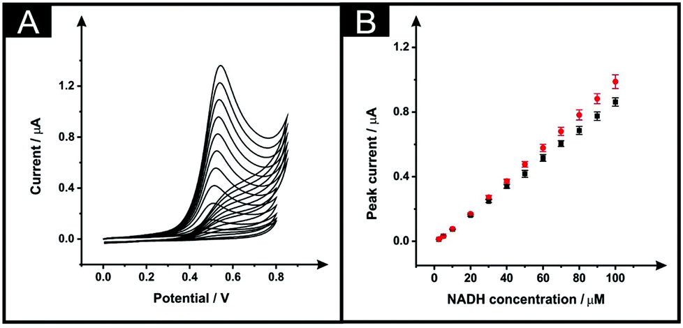 | ||
| Fig. 5 Typical cyclic voltammograms (A) as a result of increasing concentrations of NADH (2.5–100 μM)/pH 7.1 PBS using a DMF-modified ESPE (10 minutes within the solvent and a curing temperature of 100 °C for 30 minutes) and corresponding calibration plots (B) over the concentration range using an unmodified ESPE (squares) and DMF-modified ESPE (circles). Represented data indicate the average and standard deviations (N = 3). Scan rate: 50 mV s−1 (vs. SCE). | ||
Next, the electroanalytical detection of capsaicin was explored with unmodified ESPEs and with the modified counterparts, subjected to the optimised modification procedure: immersion time of 10 minutes within DMF and a curing temperature of 100 °C for 30 minutes. The redox mechanism of this interesting molecule includes first an oxidation that occurs at a potential of ∼+0.70 V (vs. SCE), as is depicted within Fig. 6A (in a 0.1 M phosphoric acid aqueous solution).28,29 In the reverse cathodic scan, the generated molecule with an o-benzoquinone unit is reduced at ∼+0.42 V to produce an o-benzenediol derivative that is subjected to an anodic process occurring at ∼+0.48 V of the second consecutive scan (at a scan rate of 50 mV s−1), which is in agreement with previous reports; no changes in the peak-to-peak separation of the voltammetric response of capsaicin on solvent modified and unmodified SPEs were evident.28,29Fig. 6A shows the response of capsaicin additions made over a concentration range of 0.25 to 10 μM where both the bare and solvent modified electrodes show linear responses (Fig. 6B) with regression equations of Ip (μA) = 0.109 μA μM−1–8.54 × 10⁻³ (μA) (R2 = 0.997; N = 3) and Ip (μA) = 0.151 μA μM−1–1.38 × 10⁻² (μA) (R2 = 0.98; N = 3) for bare ESPEs and modified ESPEs respectively. Therefore, a modest improvement within the sensitivity is observed for capsaicin with a 1.38-fold increment. Although the higher slope was obtained with the modified electrodes, the associated average standard deviation was almost twice of the bare, 12% and 7%, respectively for the modified platforms and for the bare devices (13 calibration points, N = 3). The limits of detection are found to correspond to 0.14 and 0.17 μM for bare and DMF-modified devices, respectively. These LODs are competitive and comparable to literature reports, for example, as that reported by Randviir et al.28
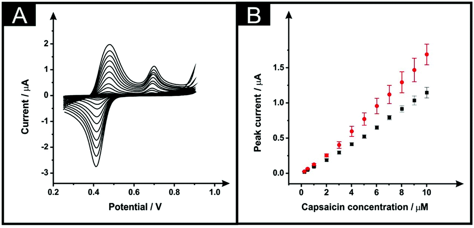 | ||
| Fig. 6 Cyclic voltammograms (A) resulting from increasing concentrations of capsaicin (0.25–10 μM)/0.1 M phosphoric acid solution using a DMF-modified ESPE (10 minutes within the solvent and a curing temperature of 100 °C for 30 minutes). The respective calibration plots (B) of the anodic signal at +0.48 V (vs. SCE) of the second consecutive cyclic voltammogram utilising unmodified ESPE (squares) and DMF-modified ESPEs (circles) are shown. Represented data indicate the average and standard deviations (N = 3). Scan rate of 50 mV s−1 (vs. SCE). | ||
Comparison with the prior literature reports
As mentioned previously, Washe et al.20 reported impressive improvements in the voltammetric signals following solvent modification where an improvement of 57-fold was reported using the redox probe potassium ferrocyanide over that of an unmodified electrode. In this paper, the increase within the effective electroactive area as evaluated in Fig. 1 (green curve) is less than 50% even when the insulative layer is attacked and partially dissolved by the DMF revealing the underlying carbon-graphite connective tracks; the electrochemical evidence of a SPE without protection of the insulating layer is depicted in Fig. 1.Further to this, if we consider the effect of DMF exposure upon the areas encompassing the working electrode of the screen-printed electrode, that is the non-conductive insulating layer utilised to cover the carbon–graphite electrode tracks and critically define the working electrode area, we observed significant shortcomings with the aim of improving just the electrochemical response of the working electrode. Fig. 7 depicts a SEM image obtained after 20 minutes of exposure to DMF, but this time focussing upon the insulating layer, which due to its polymeric composition is attacked/degraded, by the DMF. Clearly, as can be seen in the form of severe pitting, the DMF significantly distorts the insulating layer exposing the underlying carbon–graphite connective tracks. In this scenario, when the electrochemistry is performed, not only is the signal due to the working electrode area, but also the underlying exposed carbon tracks contributes which provides a significantly increased electrode area. This is in agreement with data presented in Fig. 1 (green line) where a substantially large voltammetric current was observed when the insulating layer was not protected from the DMF solvent.
 | ||
| Fig. 7 Typical SEM imaging of the working electrode (WE) and insulating layer of an ESPE after 30 minutes exposure to DMF and curing step in a fan oven at 60 °C for 30 minutes, with focus upon the insulating layer. The insulating layer of the device was in direct contact with the solvent. Note: this SPE was not protected with the DMF inert film and thus the whole sensor including part of the insulating layer was purposely immersed into DMF. | ||
Last, we revisit the work of Washe et al.,20 and re-explore their reported claims of a 57-fold improvement in the voltammetric response as demonstrated using 2 mM potassium ferricyanide. Since they report the use of an electrode area of 0.07 cm2, a 57-fold increase would correspond to an electrode area of 3.99 cm2. If we input this value into the Randles–Ševčík (eqn (4)) for a quasi-reversible electrochemical process, the expected peak current equations to ∼8.2 × 10⁻⁴ A. Inspection of Fig. 5 published in the paper by Washe et al.20 reveals that this is not the case and rather peak currents are of the ∼×10−6 A order of magnitude. This casts doubt on the hypothesis that the binder of the SPE working electrode is dissolved solely from the working electrode giving rise to a larger electrode area. Given our work above, we infer that in the work of Washe et al.20 that poor experimental control, where the insulating layer is attacked by DMF to reveal the underlying carbon tracks, highly likely contributes to the overall electrode area; this is exemplified in our work (see Fig. 7).
4. Conclusions
In this paper we have explored the effect of solvent modified SPEs evaluated using a range of electroactive compounds namely, hexaammineruthenium(III) chloride, NADH and capsaicin. In all cases, following optimisation of the solvent immersion time (step i) and curing time (step ii), for the electroanalytical sensing of NADH and capsaicin increments of 1.08-fold and 1.38-fold respectively, only are observed relative to their unmodified counterparts. Consequently, returning to the title question of this paper, Can Solvent Induced Surface Modifications Applied to Screen-Printed Platforms Enhance their Electroanalytical Performance?, in the examples presented it is not an appropriate strategy to enhance the electrochemical/electroanalytical performance of SPEs for the range of SPEs and analytes studied here.Acknowledgements
Financial support for this research was supplied by Coordenação de Aperfeiçoamento de Pessoal de Nível Superior (CAPES) – Process no 99999.001285/2014-09 and a British Council Institutional Link grant (no. 172726574).References
- R. W. Murray, A. G. Ewing and R. A. Durst, Anal. Chem., 1987, 59, A379–A390 Search PubMed.
- S. A. Wring and J. P. Hart, Analyst, 1992, 117, 1215–1229 RSC.
- A. V. Kolliopoulos, J. P. Metters and C. E. Banks, Anal. Methods, 2013, 5, 851–856 RSC.
- A. P. Ruas de Souza, C. W. Foster, A. V. Kolliopoulos, M. Bertotti and C. E. Banks, Analyst, 2015, 140, 4130–4136 RSC.
- D. A. C. Brownson, C. W. Foster and C. E. Banks, Analyst, 2012, 137, 1815–1823 RSC.
- A. P. Ruas de Souza, M. Bertotti, C. W. Foster and C. E. Banks, Electroanalysis, 2015, 27, 2295–2301 CrossRef CAS.
- C. W. Foster, J. P. Metters and C. E. Banks, Electroanalysis, 2013, 25, 2275–2282 CAS.
- Y. Xin, L. Guanghan, W. Xiaogang and Z. Tong, Electroanalysis, 2001, 13, 923–926 CrossRef CAS.
- N. Hernández-Ibáñez, L. García-Cruz, V. Montiel, C. W. Foster, C. E. Banks and J. Iniesta, Biosens. Bioelectron., 2016, 77, 1168–1174 CrossRef PubMed.
- A. Eremenko, A. Makower, W. Jin, P. Rüger and F. Scheller, Biosens. Bioelectron., 1995, 10, 717–722 CrossRef CAS PubMed.
- E. Bernalte, C. Marín Sánchez and E. Pinilla Gil, Sens. Actuators. B, 2012, 161, 669–674 CrossRef CAS.
- L. Yuan, J. Zhang, P. Zhou, J. Chen, R. Wang, T. Wen, Y. Li, X. Zhou and H. Jiang, Biosens. Bioelectron., 2011, 29, 29–33 CrossRef CAS PubMed.
- S. Cho, K.-H. Shin and J. Jang, ACS Appl. Mater. Interfaces, 2013, 5, 9186–9193 CAS.
- D. A. C. Brownson, L. C. S. Figueiredo-Filho, X. Ji, M. Gomez-Mingot, J. Iniesta, O. Fatibello-Filho, D. K. Kampouris and C. E. Banks, J. Mater. Chem. A, 2013, 1, 5962–5972 CAS.
- L. C. S. Figueiredo-Filho, D. A. C. Brownson, O. Fatibello-Filho and C. E. Banks, Electroanalysis, 2014, 26, 93–102 CrossRef CAS.
- X. Dong, X. Wang, L. Wang, H. Song, H. Zhang, W. Huang and P. Chen, ACS Appl. Mater. Interfaces, 2012, 4, 3129–3133 CAS.
- J. Wang, Electrochim. Acta, 1981, 26, 1721–1726 CrossRef CAS.
- J. M. Friedrich, C. Ponce-de-León, G. W. Reade and F. C. Walsh, J. Electroanal. Chem., 2004, 561, 203–217 CrossRef CAS.
- P. Niu, C. Fernández-Sánchez, M. Gich, C. Ayora and A. Roig, Electrochim. Acta, 2015, 165, 155–161 CrossRef CAS.
- A. P. Washe, P. Lozano-Sánchez, D. Bejarano-Nosas and I. Katakis, Electrochim. Acta, 2013, 91, 166–172 CrossRef CAS.
- A. Gomis-Berenguer, M. Gomez-Mingot, V. Montiel, A. Canals, T. Thiemann, R. O. Kadara, C. E. Banks and J. Iniesta, RSC Adv., 2012, 2, 7735–7742 RSC.
- F. E. Galdino, C. W. Foster, J. A. Bonacin and C. E. Banks, Anal. Methods, 2015, 7, 1208–1214 RSC.
- C. W. Foster, A. P. de Souza, J. P. Metters, M. Bertotti and C. E. Banks, Analyst, 2015, 140, 7598–7612 RSC.
- C. W. Foster, R. O. Kadara and C. E. Banks, Screen-Printing Electrochemical Architectures, Springer International Publishing, 1st edn, 2015 Search PubMed.
- I. Lavagnini, R. Antiochia and F. Magno, Electroanalysis, 2004, 16, 505 CrossRef CAS.
- E. P. Randviir, D. A. C. Brownson, J. P. Metters, R. O. Kadara and C. E. Banks, Phys. Chem. Chem. Phys., 2014, 16, 4598–4611 RSC.
- L. R. Cumba, C. W. Foster, D. A. C. Brownson, J. P. Smith, J. Iniesta, B. Thakur, D. R. do Carmo and C. E. Banks, Analyst, 2016 10.1039/C6AN00167J.
- E. P. Randviir, J. P. Metters, J. Stainton and C. E. Banks, Analyst, 2013, 138, 2970–2981 RSC.
- R. T. Kachoosangi, G. G. Wildgoose and R. G. Compton, Analyst, 2008, 133, 888–895 RSC.
- A. V. Kolliopoulos, J. P. Metters and C. E. Banks, Anal. Methods, 2013, 5, 3490–3496 RSC.
Footnote |
| † Electronic supplementary information (ESI) available. See DOI: 10.1039/c6an00440g |
| This journal is © The Royal Society of Chemistry 2016 |