
 Open Access Article
 This Open Access Article is licensed under a
 Creative Commons Attribution 3.0 Unported Licence
A tunable Au core–Ag shell nanoparticle tip for tip-enhanced spectroscopy†
Woong
Kim‡
a,
Nara
Kim‡
b,
Eunbyoul
Lee§
c,
Duckhoe
Kim¶
a,
Zee
Hwan Kim
*b and
Joon
Won Park
*a
aDepartment of Chemistry, Pohang University of Science and Technology, Pohang, 790-784, Republic of Korea. E-mail: jwpark@postech.ac.kr
bDepartment of Chemistry, Seoul National University, Seoul 151-742, Korea. E-mail: zhkim@snu.ac.kr
cDepartment of Chemistry, Korea University, Seoul 136-701, Korea
First published on 17th February 2016
Abstract
A single Au nanoparticle (NP) with a diameter of 5 nm was transferred to the end of a Si-tip through a picking process, and an Ag shell with a controlled thickness was formed on the Au core. By carrying out tip-enhanced Raman scattering (TERS) measurements on biphenyl-4-thiol (BPT) with the Au@Ag NP–tip (overall diameter of 22–60 nm), we confirm that such tips show a plasmonic local-field enhancement which is sufficient for tip-enhanced spectro-microscopy.
Introduction
Tip-enhanced spectroscopy (TES)1–4 employs plasmonic field enhancement and confinement at the end of a scanning probe (tip) to provide nanometric (∼10 nm) spectro-microscopy images of nanostructures and single molecules.5 A major challenge is thus the reproducible fabrication of tips with an idealized shape and composition for optimized field enhancement.Therefore, researchers have explored numerous forms of tips,6,7 including metal-coated Si-tips,8,9 etched metal wires,10,11 and nanostructure-attached tips,12–16 to achieve better field enhancement and enhanced reproducibility. A particularly promising form of the tip is a dielectric tip with a plasmonic nanoparticle (NP) attached to the end, which not only offers a dipole plasmon resonance response but also provides structural tunability of the tip-end.
The NP–tip is usually fabricated by picking up a relatively large NP (50–100 nm) by a tip that is pre-functionalized with “glue” (such as organic thiols17 or polyethyleneimine18). In this method, however, precise and reproducible positioning of the NP with respect to the tip axis is hard to achieve because the pickup pathway of relatively large NPs is not well controlled. Better control of the pathway could be achieved if we could directly grow a single crystal NP on the tip.
Previously, we reported that a dendron-modified atomic force microscopy (AFM) tip effectively suppressed multiple DNA–DNA interactions and guaranteed single DNA–DNA interactions during the force measurement.19–21 In particular, the approach demonstrated that picking a single-stranded DNA while concomitantly avoiding multiple DNAs was efficient (approximately 75% yield), and a AuNP conjugated with the DNA was visualized with a transmission electron microscope.22–24
Here, Au@Ag NP–tips that are useful for TES were made by picking a single-seed AuNP (5 nm) and subsequently growing the NP with a silver-enhancing solution. The first step is transferring a single-seed AuNP from a solid surface to the end of a tip using different chemical unbinding forces between a short DNA and a long one (see ESI, Fig. S1† for the detailed procedure). The size of the Au@Ag NPs could be systematically controlled by varying the growth conditions. With tip-enhanced Raman scattering (TERS) measurements, we demonstrate that such tips show plasmonic field enhancement useful for TES.
Experimental section
General
The silane coupling agent N-(3-(triethoxysilyl)-propyl)-O-polyethyleneoxide urethane (TPU) was purchased from Gelest. Seed gold nanoparticles (5 nm) were purchased from Ted Pella. Oligonucleotides were purchased from IDT. The atomic force microscopy probes employed for the picking process were purchased from BudgetSensors (Contact-G, see Fig. S2† for detailed characteristics of the employed AFM tip). A detailed procedure for the preparation of dendron-modified picking tips and wafer substrates was reported elsewhere.19,22 The picking process was performed using a ForceRobot 300 AFM (JPK instrument). Transmission electron microscopy (TEM, JEM-1011, JEOL) was used to image the tips. Biphenly-4-thiol (97%, Sigma Aldrich), silver nitrate (99.9999% Sigma-Aldrich), and sodium L-ascorbate (BioReagent, Sigma-Aldrich) were used to synthesize the Au@Ag NPs. All solutions were freshly prepared before use. A clean cover glass was coated with Au (10 nm)/Ti (2 nm) using an e-beam evaporator and was used as a sample substrate for the TERS measurement. The substrate was immersed in a solution of biphenyl-4-thiol (BPT, 25 mM in ethanol) for ca. 2 h to produce a fully saturated organic monolayer and then rinsed with ethanol to remove excess BPT.Set-up for tip-enhanced Raman scattering
The TERS microscope (see ESI, Fig. S3† for a detailed layout) consisted of an inverted microscope (IX71, Olympus), a Raman spectrometer (Triax 320, Horiba; DU-401, Andor Tech) and an atomic force microscope (AFM, XE-120, Park Systems) operating under the contact mode. The linearly polarized laser beam (wavelength of 532 nm, Nd:YAG) was converted to radially polarized light using a radial polarizer (Nanophoton, ZPol-532-QzM-4). The radially polarized beam25,26 provides the enhanced z-polarization component (parallel to the tip axis) of the electric field at the tip–sample junction, enhancing the TERS signal. The beam was focused onto the tip through an objective lens (oil immersion, NA = 1.46), and the Raman signal was collected through the same objective lens (ESI, Fig. S3†).Results and discussion
The Au@Ag NP–tip fabrication consists of a three-step process (initial enhancement, annealing, and final enhancement). A single-seed AuNP (5 nm) was transferred onto the end of the tip of the dendron-modified AFM tip (see Fig. 1D. See also Kim et al.22 for the detailed procedure). The typical success rate for the pickup process exceeds 70%. The seed AuNP on the tip was adhered through a single DNA duplex, and it could be detached from the tip during repeated handling. We found that thermal annealing (heating in air at 500 °C for 10 min) significantly enhanced the adhesion, and annealing after the initial enhancement facilitated the NP growth to the targeted size.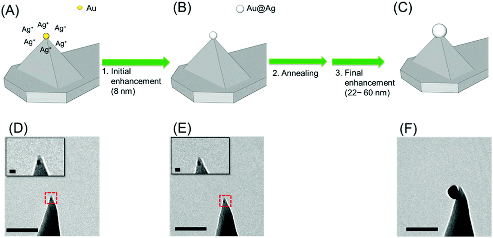 | ||
| Fig. 1 Tip preparation steps and TEM image of the thus-prepared tips. First, a tip with a 5 nm seed AuNP (A) is immersed in AgNO3/sodium L-ascorbate solution to grow a small Au@Ag NP (B). The tip is thermally annealed and Ag-enhanced again to generate a fully grown Au@Ag NP at the tip end (C). (D), (E), and (F) are representative TEM images of tips with a seed AuNP (5 nm, D), after the initial enhancement and annealing (size: 7.6 ± 0.3 nm, E), and after the final enhancement for 1 h (the size: 35.0 ± 0.3 nm, F). The inset images in (D) and (E) are zoomed-in images of the regions (dotted squares) in the corresponding TEM images. Scale bars: 100 nm (main images) 10 nm (inset images). | ||
After the initial enhancement and thermal annealing, the tip was immersed (∼10 min) in a silver-enhancing solution (a mixture of 200 μL of 1.0 mM AgNO3 and 50 μL of 1.0 mM sodium L-ascorbate in a phosphate-buffered saline solution at pH 7.4). A shell of Ag was formed (total thickness of 8 nm, Fig. 1B and E) on the surface of the seed AuNP due to the lower reduction potential of Ag compared with that of Au.
We observed that a strong reductant such as sodium borohydride produces AgNPs non-specifically at various positions on the AFM tip. The employed sodium L-ascorbate enhanced the Ag selectively on the seed AuNP and minimized deposition of AgNPs on other parts of the AFM tip. Additionally, varying the immersion time offered effective control of the thickness of the Ag shell. Fig. 2 is a collection of representative TEM images of the fabricated Au@Ag NP–tips with various particle sizes, featuring the enhanced adhesion properties (vide ante) and the size control. Typically, 7 or 8 out of 10 seed NP–tips successfully formed a single Au@Ag NP at the tip apex (average yield = 75%). Overall, we find that this three-step procedure is far more effective than a two-step process (without the annealing) in terms of the success rate and mechanical durability.
 | ||
| Fig. 2 Representative TEM images of TES tips with Au@Ag NPs with various sizes (scale bar: 100 nm, see ESI, Fig. S4† for the measurement of the diameter of NP). (A) 24 ± 0.5 nm, (B) 28 ± 0.3 nm, (C) 34 ± 0.7 nm, (D) 50 ± 0.4 nm, (E) 55 ± 0.7 nm, (F) 60 ± 0.5 nm. | ||
While the Au seed NP used for the growth process is spherical, the enhancement with the silver ion may produce a truncated sphere or a hemisphere on the tip surface because of the geometrical constraint. In addition, there may be an Au–Si alloying27–29 and re-shaping during the annealing step. These may overall result in the shape of the NP that is not smooth and non-spherical (Fig. 2-D).
To confirm that the Au@Ag NP on the tip acts as a near-field light source for TES, we carried out the TERS measurements on the BPT monolayer on an Au thin film (Fig. 3). To minimize the deleterious effect of the oxidized Ag layer formation onto the tip-end, the tip was briefly immersed in the silver enhancing solution (3 min) just before the TERS measurements. Through independent measurements, we confirmed that such a last-minute treatment did not induce a noticeable change in the Au@Ag NP size. Fig. 4 shows the TERS spectra of the BPT sample (see ESI, Fig. S5†) collected with tips of various Au@Ag NP sizes (also shown in comparison is the spectrum (black) obtained without the tip (tip-off), reflecting residual surface-enhanced Raman scattering (SERS) signal arising from the roughness of Au film).
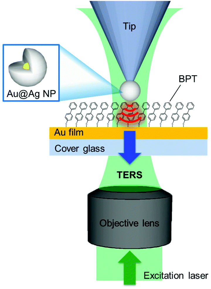 | ||
| Fig. 3 Measurement of TERS. The monolayer of biphenyl-4-thiol (BPT) is self-assembled on an Au coated cover glass. Laser beam is focused on the Au@Ag NP attached tip through an objective lens and the Raman radiation is collected through the same objective lens. | ||
 | ||
| Fig. 4 A set of BPT TERS spectra with (tip-on, colored lines) and without (tip-off, black line) Au@Ag NP–tips. The same BPT sample was used for all of the measurements. Each spectrum was obtained with a laser power of 20 μW, and the integration time was 180 s. For the ease of viewing, each of the spectra is vertically offset. | ||
As seen in the spectra, the tips show a pronounced signal enhancement for the major Raman peaks of BPT (1585, 1573, 1288 cm−1 (ring stretching), and 1174 cm−1 (C–H bending), see ESI, Table S1† for the peak assignments). Among the 27 tips (diameter > 20 nm) employed, 19 tips were found to be TERS active. Furthermore, the overall TERS signal (tip-on) increases with the Au@Ag NP diameter (see also Fig. 5A). This trend is fully consistent with analogous SERS measurements30–32 on the NP-monolayer of molecule-thin film structures. Fig. 5 shows the experimental TERS enhancement factor (EF, estimated for the peaks at 1585 and 1573 cm−1, see ESI, page S7 and Fig. S6† for the definition on experimental estimation of EFs), which is plotted as a function of the Au@Ag NP-diameter, showing a systematic increase in EF with the Au@Ag NP-diameter. In general, an increase in NP-diameter enhances the polarizability of the tip-end and thus increases the local field at the tip through the tip–sample coupling. The general trend and the values of EFs agree with the electrodynamic model (Fig. 5B, see ESI, page S8 and Fig. S7† for details about the simulation of EFs) of the Raman enhancement calculated by the finite-difference time-domain (FDTD, Lumerical Solutions Inc.) calculation on the Au@Ag NP-molecule–Au thin film junction. In the simulation, the tip is modelled as an isolated core–shell structure with a spherical Au-core diameter of 5 nm surrounded by a spherical Au-shell with a varying thickness (t) to give an overall diameter of 2t + 5 nm. The substrate is modelled as a perfectly flat Au thin-film (with a thickness of 10 nm) and a glass (with an infinite thickness). The tip–sample distance is fixed at 1.25 nm. A p-polarized plane-wave at λ = 532 nm (E0, which approximately model the radically polarized illumination) is radiated, and the local field (Eloc) at the substrate surface is calculated. The SERS enhancement factor is calculated by spatially averaging the |Eloc/E0|4 factor around the center of hotspots. The dielectric functions employed is from Palik et al.33
 | ||
| Fig. 5 Change in the TERS enhancement with the increase in the overall Au@Ag NP-diameter. (A) Experimental enhancement factor derived from the TERS peaks of BPT at 1573 & 1585 cm−1. The x-error bars represent the statistical variation and uncertainty in the diameter of the Au@Ag NP, arising from the non-spherical shapes of the Au@Ag NPs. The y-error bars represent the variation of TERS signals obtained from different positions on the sample surface. (B) FDTD simulated enhancement factors calculated for Au@Ag NPs of various diameters in close contact with the Au thin film (see inset image for the simulated local field enhancement, |E/E0|4, where E and E0 are the enhanced local field and the incident field, respectively, evaluated for Au@Ag NP of an overall diameter of 60 nm (Au core diameter of 5 nm and Ag shell thickness of 27.5 nm; overall diameter: 60 nm) around the junction). | ||
In particular, in both the experiment and simulation, doubling the diameter of the NP leads to the increase in EF by a factor of ∼5. Based on the simulation, we find that the Au@Ag core–shell structure shows a slightly smaller EF relative to the monolithic AgNP with the same size, yet it retains a similar dipolar plasmonic field. The simulation overestimates the experimental EF by a constant factor of ∼10. This discrepancy may originate from the oxidation of the Ag-shell as well as from the systematic error in the experimental EF estimate. Nevertheless, it does clearly show that the fabricated Au@Ag NP–tip acts as a viable near-field probe with a significant local field enhancement.
Conclusions
Several Au@Ag NPs were synthesized selectively on an AFM tip-end, and the size of the NP can be controlled by changing the reaction time in the silver-enhancing solution. With the TERS measurements, we have verified that such tips can be used as a plasmonically active near-field probe.In terms of TERS-performance, the NP–tip we have fabricated has several weaknesses compared with the state-of-art TERS probes reported.34 The enhancement factors of ∼104 are not exceptional compared with the current state-of-art TERS probes.35,36 This arises from a smooth near-spherical tip-shape without any sharp protrusion, and also from the Au@Ag core–shell structure. In particular, we found from the simulation (see ESI, Fig. S8 and S9†) that the Au@Ag core–shell structure has an ∼10 times weaker TERS signal than the monolithic Ag sphere with a comparable diameter, due to the plasmon damping of the Au-core. We estimate that the nominal spatial resolution of the current tip is around 50–100 nm. This limited resolution arises from a relatively large dimension of the tip-end that is in contact with the sample surface. We note that an increase in the diameter of the NP–tip increases the EF, yet it decreases the achievable spatial resolution (see the ESI for simulation, Fig. S10†).
Despite the above shortcomings in terms of EF and spatial resolution, the current approach has a unique strength in the reproducibility of fabrication and extendibility, which are not easily achievable from other forms of tips. In particular, the method shows the possibility that the NP–tip for the TES end can be reproducibly (>70%) fine-tuned by wet chemistry. Furthermore, interference of the linker molecules (in our case DNA bases) in the spectra is found to be negligible.
The morphology of the final NP–tip is determined by the morphology of the seed, and the subsequent growth chemistry, both of which can be separately optimized, as recently demonstrated by Kim et al.14 Such fine-control is not easily achievable in mechanical37 or photochemical NP–tip fabrication.7
We thus believe that the current preparation procedure can be extended to NPs with various geometries such as hollow shells or octahedra, which may offer increased sensitivity and spatial resolution in tip-enhanced spectro-microscopy in addition to the improved reproducibility for the TES activities.
Acknowledgements
J. W. P. acknowledges the Brain Research Program (2015030964) of the National Research Foundation (NRF) of Korea and the Converging Research Center Program (2015K000211) of the Ministry of Science, ICT, and Future Planning, Korea. Z. H. K. and N. K. were supported by BioNano Health-Guard Research Center funded by the Ministry of Science, ICT & Future Planning (MSIP) of Korea as Global Frontier Project (H-GUARD_2013M3A6B2078947) and the Research Resettlement Fund for the New Faculty of SNU.References
- A. Hartschuh, Angew. Chem., Int. Ed., 2008, 47, 8178–8191 CrossRef CAS PubMed.
- N. Mauser and A. Hartschuh, Chem. Soc. Rev., 2014, 43, 1248–1262 RSC.
- T. W. Johnson, Z. J. Lapin, R. Beams, N. C. Lindquist, S. G. Rodrigo, L. Novotny and S. H. Oh, ACS Nano, 2012, 6, 9168–9174 CrossRef CAS PubMed.
- L. Novotny and S. J. Stranick, Annu. Rev. Phys. Chem., 2006, 57, 303–331 CrossRef CAS PubMed.
- R. Zhang, Y. Zhang, Z. C. Dong, S. Jiang, C. Zhang, L. G. Chen, L. Zhang, Y. Liao, J. Aizpurua, Y. Luo, J. L. Yang and J. G. Hou, Nature, 2013, 498, 82–86 CrossRef CAS PubMed.
- W. Bao, M. Melli, N. Caselli, F. Riboli, D. S. Wiersma, M. Staffaroni, H. Choo, D. F. Ogletree, S. Aloni, J. Bokor, S. Cabrini, F. Intonti, M. B. Salmeron, E. Yablonovitch, P. J. Schuck and A. Weber-Bargioni, Science, 2012, 338, 1317–1321 CrossRef CAS PubMed.
- T. Umakoshi, T. A. Yano, Y. Saito and P. Verma, Appl. Phys. Express, 2012, 5, 052001 CrossRef.
- T. Ichimura, S. Fujii, P. Verma, T. Yano, Y. Inouye and S. Kawata, Phys. Rev. Lett., 2009, 102, 186101 CrossRef PubMed.
- E. M. van Schrojenstein Lantman, T. Deckert-Gaudig, A. J. G. Mank, V. Deckert and B. M. Weckhuysen, Nat. Nanotechnol., 2012, 7, 583–586 CrossRef CAS PubMed.
- J. Stadler, T. Schmid and R. Zenobi, Nano Lett., 2010, 10, 4514–4520 CrossRef CAS PubMed.
- B. Ren, G. Picardi and B. Pettinger, Rev. Sci. Instrum., 2004, 75, 837–841 CrossRef CAS.
- P. Bharadwaj, P. Anger and L. Novotny, Nanotechnology, 2007, 18, 044017 CrossRef.
- T. Kalkbrenner, U. Hakanson, A. Schädle, S. Burger, C. Henkel and V. Sandoghdar, Phys. Rev. Lett., 2005, 95, 200801 CrossRef CAS PubMed.
- W. Kim, N. Kim, J. W. Park and Z. H. Kim, Nanoscale, 2016, 8, 987–994 RSC.
- Y. Gan, Rev. Sci. Instrum., 2007, 78, 081101 CrossRef PubMed.
- C. Leiterer, T. Deckert-Gaudig, P. Singh, J. Wirth, V. Deckert and W. Fritzsche, Electrophoresis, 2015, 36, 1142–1148 CrossRef CAS PubMed.
- I. U. Vakarelski and K. Higashitani, Langmuir, 2006, 22, 2931–2934 CrossRef CAS PubMed.
- T. Kalkbrenner, M. Ramstein, J. Mlynek and V. Sandoghdar, J. Microsc., 2001, 202, 72–76 CrossRef CAS PubMed.
- J. Jung, B. J. Hong, W. Zhang, S. J. Tendler, P. M. Williams, S. Allen and J. W. Park, J. Am. Chem. Soc., 2007, 129, 9349–9355 CrossRef PubMed.
- D. Kim and O. Sahin, Nat. Nanotechnol., 2015, 10, 264–269 CrossRef CAS PubMed.
- P. Hinterdorfer and Y. F. Dufrene, Nat. Methods, 2006, 3, 347–355 CrossRef CAS PubMed.
- D. Kim, N. K. Chung, J. S. Kim and J. W. Park, Soft Matter, 2010, 6, 3979–3984 RSC.
- D. Kim, N. K. Chung, S. Allen, S. J. Tendler and J. W. Park, ACS Nano, 2012, 6, 241–248 CrossRef CAS PubMed.
- K. Liu, Y. Song, W. Feng, N. N. Liu, W. K. Zhang and X. Zhang, J. Am. Chem. Soc., 2011, 133, 3226–3229 CrossRef CAS PubMed.
- H. Ishitobi, I. Nakamura, T. A. Kobayashi, N. Hayazawa, Z. Sekkat, S. Kawata and Y. Inouye, ACS Photonics, 2014, 1, 190–197 CrossRef CAS.
- A. M. Chizhik, R. Jager, A. I. Chizhik, S. Bar, H. G. Mack, M. Sackrow, C. Stanciu, A. Lyubimtsev, M. Hanack and A. J. Meixner, Phys. Chem. Chem. Phys., 2011, 13, 1722–1733 RSC.
- S. Hazra, S. Pal, S. Kundu and M. K. Sanyal, Appl. Surf. Sci., 2001, 182, 244–250 CrossRef CAS.
- B. Ressel, K. C. Prince, S. Heun and Y. Homma, J. Appl. Phys., 2003, 93, 3886–3892 CrossRef CAS.
- F. Ruffino, A. Canino, M. G. Grimaldi, F. Giannazzo, F. Roccaforte and V. Raineri, J. Appl. Phys., 2008, 104, 024310 CrossRef.
- W. H. Park and Z. H. Kim, Nano Lett., 2010, 10, 4040–4048 CrossRef CAS PubMed.
- K. Kim, H. B. Lee and K. S. Shin, Spectrochim. Acta, Part A, 2013, 100, 10–14 CrossRef CAS PubMed.
- K. Kim and K. S. Shin, Anal. Sci., 2011, 27, 775–783 CrossRef CAS PubMed.
- E. D. Palik, Handbook of optical constants of solids, Academic press, 1998 Search PubMed.
- C. Chen, N. Hayazawa and S. Kawata, Nat. Commun., 2014, 5, 3312 Search PubMed.
- N. Jiang, E. T. Foley, J. M. Klingsporn, M. D. Sonntag, N. A. Valley, J. A. Dieringer, T. Seideman, G. C. Schatz, M. C. Hersam and R. P. Van Duyne, Nano Lett., 2012, 12, 5061–5067 CrossRef CAS PubMed.
- K. Uetsuki, P. Verma, P. Nordlander and S. Kawata, Nanoscale, 2012, 4, 5931–5935 RSC.
- I. Maouli, A. Taguchi, Y. Saito, S. Kawata and P. Verma, Appl. Phys. Express, 2015, 8, 032401 CrossRef CAS.
Footnotes |
| † Electronic supplementary information (ESI) available: Illustration of a single-seed nanoparticle picking process, characteristics of the AFM tip, TERS set-up, information of size measurement of NP, normal Raman signal, experimental and FDTD simulation of enhancement factors, FDTD simulation of AgNP, simulated spatial resolution of NP-tip as a function of the diameter of tip-end and peak assignments of TERS spectra. See DOI: 10.1039/c6an00035e |
| ‡ These authors contributed equally to this work. |
| § Current address: Doosan Corporation Electro-Materials, Sujigu, Gyeonggi do, Korea. |
| ¶ Current address: The Department of Biological Sciences, Columbia University, New York, USA. |
| This journal is © The Royal Society of Chemistry 2016 |