
 Open Access Article
 This Open Access Article is licensed under a
 Creative Commons Attribution 3.0 Unported Licence
Self-limiting atomic layer deposition of barium oxide and barium titanate thin films using a novel pyrrole based precursor†
Shinjita
Acharya‡
*a,
Jan
Torgersen‡
*a,
Yongmin
Kim
a,
Joonsuk
Park
b,
Peter
Schindler
a,
Anup L.
Dadlani
c,
Martin
Winterkorn
a,
Shicheng
Xu
 a,
Stephen P.
Walch
a,
Takane
Usui
d,
Christian
Schildknecht
e and
Fritz B.
Prinz
ab
a,
Stephen P.
Walch
a,
Takane
Usui
d,
Christian
Schildknecht
e and
Fritz B.
Prinz
ab
aDepartment of Mechanical Engineering, Stanford University, CA 94305, USA. E-mail: shinjita@stanford.edu; jtorgers@stanford.edu
bDepartment of Material Science and Engineering, Stanford University, CA 94305, USA
cDepartment of Chemistry, Stanford University, CA 94305, USA
dBASF Corporation, Union, NJ 07083, USA
eCalifornia Research Alliance (CARA), BASF Corporation, Berkeley, CA 94720, USA
First published on 22nd December 2015
Abstract
Barium oxide (BaO) is a critical component for a number of materials offering high dielectric constants, high proton conductivity as well as potential applicability in superconductivity. For these properties to keep pace with continuous device miniaturization, it is necessary to study thin film deposition of BaO. Atomic layer deposition (ALD) enables single atomic layer thickness control, conformality on complex shaped substrates, and the ability to precisely tune stoichiometry. Depositing multicomponent BaO containing ALD films in a self-limiting manner at low temperatures may extend the favorable bulk properties of these materials into the ultrathin film regime. Here we report the first temperature and dose independent thermal BaO deposition using a novel pyrrole based Ba precursor (py-Ba) and water (H2O) as the co-reactant. The growth per cycle (GPC) is constant at 0.45 Å with excellent self-terminating behavior. The films are smooth (root mean squared (RMS) roughness 2.1 Å) and contain minimal impurities at the lowest reported deposition temperatures for Ba containing films (180–210 °C). We further show conformal coating of non-planar substrates (aspect ratio ∼ 1![[thin space (1/6-em)]](https://www.rsc.org/images/entities/char_2009.gif) :2.5) at step coverages above 90%. Intermixing TiO2 ALD layers, we deposited amorphous barium titanate with a dielectric constant of 35. The presented approach for infusing self-terminating BaO in multicomponent oxide films may facilitate tuning electrical and ionic properties in next-generation ultrathin devices.
:2.5) at step coverages above 90%. Intermixing TiO2 ALD layers, we deposited amorphous barium titanate with a dielectric constant of 35. The presented approach for infusing self-terminating BaO in multicomponent oxide films may facilitate tuning electrical and ionic properties in next-generation ultrathin devices.
Introduction
Incorporating barium oxide (BaO) with transition metal oxides forms interesting multinary compounds with mostly perovskite crystal structures. These electroceramics exhibit high dielectric constants (BaTiO31,2 and BaSrTiO33), high proton conductivity (Y doped BaZrO34,5) and, depending on the crystal arrangement, ferroelectricity,5 piezoelectricity6 and photorefractive effects.6 These structures can be applied to low temperature superconductors,7,8 solar cells,9,10 high-k capacitors11 and fuel cells.4 Atomic level control of the films’ thickness, composition and crystal structure can be significant for device miniaturization and for verifying theoretically predicted properties in the ultrathin film regime.12 However, it necessitates a manufacturing technique capable of fabricating pin-hole free films with the aforementioned characteristics. In addition, conformal coverage on complex shaped structures3,13,14 is desirable.Atomic layer deposition (ALD) is well suited to address these challenges.15,16 Unique self-limiting growth characteristics allow for the conformal deposition of various metals, insulators and semiconductors (in both, crystalline and amorphous phases),16 onto a variety of substrates including high aspect ratio structures17 and thermally fragile polymers.18,19 In ALD, metal precursors primarily determine the nature of the surface reactions, hence governing deposition and quality of the thin film. They also control surface chemistries crucial to drive the self-limiting growth mode, i.e. the ability to reach surface saturation at each reaction step.
For ALD of multicomponent films containing BaO, the low volatility, poor thermal stability and weak surface functional group reactivity of commercially available Ba precursors has been the bottleneck for deposition of high quality films with uniform stoichiometry.1 Only cyclopentadienyl (cp-Ba)-type precursors were used for ALD of barium containing oxides with H2O as a co-reactant.4,20 Using cp-Ba, multicomponent perovskite materials, such as BaTiO3 (BTO),1,2,21 BaZrO34,5 and Ba(1−x)SrxTiO322,23 films can be grown in a self-limiting manner, independent from the precursor dosage. Self-limiting growth of binary BaO, the critical underlying framework for these films, is yet to be reported. One of the limitations with cp-type precursors is that they exhibit chemical vapor deposition (CVD)-like behavior: they can readily react to any oxygen-containing species, not requiring other oxidants.24 To precisely control the growth rate as well as the chemical composition, all binary oxide depositions in a multicomponent system should be done under distinct ALD windows. Whereas TiO225 and ZrO2,26 thin films have been deposited in a self-terminating manner on complex shaped substrates, this has not been shown with BaO. The development of a self-limiting deposition process for BaO is crucial for controlling BTO and BZO deposition. Hence, after roughly 15 years of research and continuous improvement on cp-type Ba precursors, an alternative precursor is worth investigating.
In this report, we establish the ALD window for depositing BaO using a novel pyrrole based barium compound (py-Ba). This precursor facilitates deposition at substrate temperatures as low as 180 °C. Using H2O as the oxidant, we show the independence of the growth per cycle (GPC) with respect to precursor dosage as well as the number of half-cycles within a full cycle. Excellent thickness uniformity, low roughness, and minimal impurity content are manifest of the high thin film quality. The BaO has been shown to grow conformally on non-planar substrates (aspect ratio, AR ∼ 1:2.5), with step coverage over 90%. To show the potential of py-Ba to fabricate multicomponent films, we deposit BTO. Here the deposition of binary BaO under ALD conditions enables the best dielectric performance of amorphous BTO based metal–insulator–metal (MIM) devices so far.
Experimental
We used a customized reactor for four inch wafers equipped with automated temperature, pressure and mass flow controllers (MFCs, Alicat Scientific, USA) for the deposition of BaO and BTO films (Fig. 1). BASF (Ludwigshafen, Germany) developed and supplied the proprietary py-Ba precursor. Alfa-Aesar (USA) supplied titanium(IV) isopropoxide (TTIP). All precursors and oxidants were kept in 50 cm3 stainless steel sample cylinders and heated to 175 °C (py-Ba, based on thermo-gravimetric analysis (TGA), Fig. S1, ESI†) and 70 °C (TTIP), respectively. The chamber had three inlet ports. The first attached py-Ba to the chamber and was backed by an Ar line. The second port connected the manifold containing the oxidant (H2O), trimethylaluminium (TMA) and the purge gas (Ar). The third port attached TTIP. A constant flow of 10 sccm of Ar flowing through the manifold resulted in a chamber pressure of 0.6 Torr (measured by a Pirani gauge, Kurt Lesker Company, USA). The chamber exhaust was connected to a stop valve, pressure gauge (both Kurt J. Lesker, USA) and a roughing pump (Edwards, USA). Standard pneumatic ALD valves (Swagelok, USA) pulsed all precursors and the oxidant into the chamber.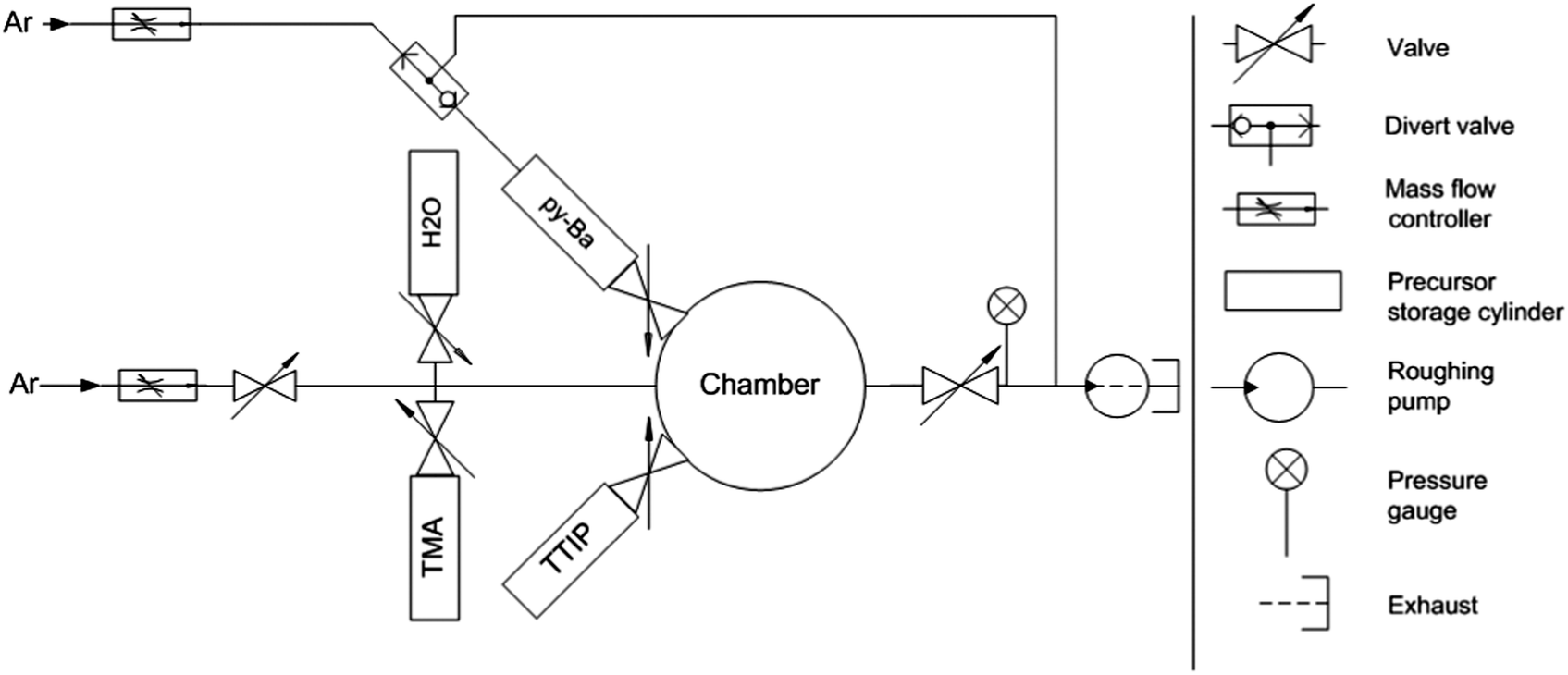 | ||
| Fig. 1 Schematic of customized ALD reactor for deposition of BaO and BTO films. | ||
We deposited BaO films on 500 μm thick p-doped 〈100〉 Si wafers. For electrical measurements, an MIM structure with BTO as dielectric layer was deposited onto 200 nm thick e-beam evaporated Ru (Innotec, USA) on a 500 μm thick 〈100〉 Si wafer with a 100 nm thermal SiO2 insulating layer. H2O pulses prior to the deposition resulted in an interfacial layer of conductive RuO2, which served as back electrode.27 Top electrodes (anodes) consisting of patterned, 200 nm thick Pt pads (680 × 680 μm2) were evaporated onto the BTO films (e-beam evaporation, Kurt Lesker company, USA). The equivalent oxide thicknesses (EOTs), given by EOT = tBTO × (εSiO2/εBTO), capacitance–voltage (C–V) characteristics and dielectric constants of ALD films were measured using an LCR meter. Current–voltage (I–V) measurements were conducted using a voltage source ammeter (Keithley instruments, USA). Leakage currents were measured for applied biases between 0 and +1.6 V.
The trenches on the Si substrate were fabricated by reactive ion etching (RIE) in an inductively coupled plasma (ICP) system (TCP 9400, Lam Research, USA), using hydrogen bromide (HBr), chlorine (Cl2) and oxygen (O2) as etch gases. Positive photoresist, patterned by in-line lithography, was used as the etch mask and afterwards removed using heated piranha solution (9:1 H2SO4:H2O2 at 120 °C), followed by a polymer descum using O2 plasma.
Elemental compositions of the films were analyzed by X-ray photoelectron spectroscopy (XPS) in a PHI-Versaprobe (Physical electronics, USA) using Al Kα radiation (1486 eV). The instrument was equipped with Ar ion sputter guns for surface cleaning and depth profile analysis. Ar sputtering (2 kV, 1 μA, 1 × 10⁻⁷ Torr) was ∼6 nm min−1. The thickness of BaO and BTO films was determined according to an optical model fit to ellipsometer (Woollam, USA)28 measurements, and roughness was quantified via atomic force microscopy (AFM) (JSPM 5200, JEOL, USA). The thickness was confirmed using transmission electron microscopy (TEM) (Titan ETEM 300 kV, FEI, USA) and X-ray reflectivity (X'Pert Pro, PANalytical, Netherlands). The sample for cross-sectional TEM (FEI 80-300 Titan) analysis was prepared using focused ion beam (FEI Helios) with lift-out technique. All high resolution TEM (HRTEM) images were taken at 300 kV accelerating voltage with spherical aberration correction. For BaO thickness measurement, lack of contrast difference between amorphous C and BaO films made it difficult to directly find out the thickness of the films, hence, scanning TEM electron energy loss spectroscopy (STEM-EELS) was performed across the interface at the top, side, and bottom of the trench. The STEM-EELS acquisition condition was 300 kV STEM probe with GIF Quantum 966 EELS spectrometer, point size 0.3 nm, exposure time from 1 to 3 s, 0.1 eV/channel energy dispersion for Si L & Ba M peaks around 99 eV and 781 eV respectively.
We performed ab initio calculations to evaluate the precursor dissociation energies to the metal center. We generated the starting geometries manually and optimized them using the universal force field (UFF).29 Using Becke's three parameter exchange functional and the Lee–Yang–Parr gradient functional (B3LYP)30,31 as implemented in the Gaussian09 package,32 we performed geometry optimizations to find energy minima (stationary points). We chose the Los Alamos basis set LANL2DZ (effective core potential and a double-ζ valence shell)33 for the Ba center and the cc-pvdz, Dunning's correlation consistent basis set for all other atoms.34
Results and discussion
A. Growth of binary BaO films
One cycle of BaO deposition consisted of one py-Ba dosing sequence with variable boosting35 duration, dwell time of 20 s and subsequent release for 2 s. 10 H2O (oxidant) doses (1 s each) separated by purging steps (30 s) followed this step. Boosting with Ar gas increased the total canister pressure, assisting the precursor vapor delivery into the chamber. We will henceforth compare the amount of precursor delivered to the chamber by the total pressure difference between the precursor dose and the base pressure of the chamber (see ESI† for the details). Using a constant boosting time (2 s) followed by one py-Ba dosing sequence per cycle, we deposited 100 cycles of BaO in every run. We varied the substrate temperature from 180 °C (slightly above precursor temperature) to 250 °C to establish the ALD temperature regime for py-Ba. Physical thicknesses of the films measured using spectroscopic ellipsometry28 revealed the GPC as shown in Fig. 2. We identify a constant growth rate plateau between 180 and 210 °C (0.45 Å per cycle) as shown in Fig. 2a; however the rate decreased as the temperature increased to 225 °C. At 250 °C, we observed no deposition. This may indicate desorption of the surface species at higher temperatures, as for ALD of Al2O336 and SrO.37 ALD temperature regime of this precursor (180 °C and 210 °C) is lower than for previously reported BaO containing films.4,21 We optimized the growth conditions at 210 °C substrate temperature, well within the established ALD window of the precursor. The lower thermal budget of deposition is advantageous for applications where the underlying materials, for example organic transistors, are temperature sensitive. Usually the hygroscopic nature of BaO leads to hydroxide formation during the H2O pulse,1 which we could overcome with sufficient purge preventing side-reactions.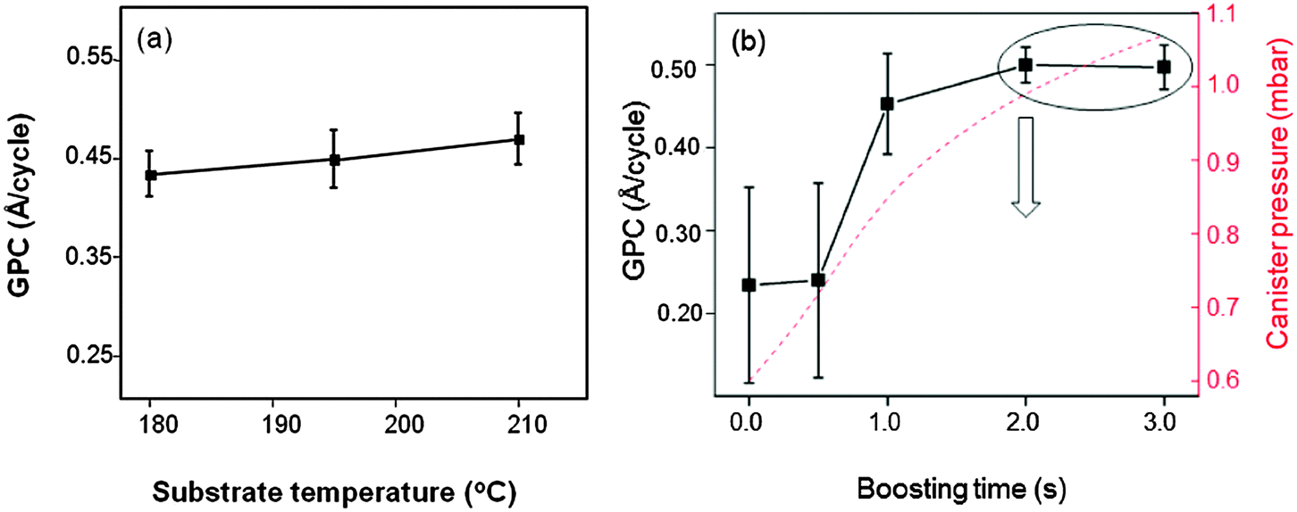 | ||
| Fig. 2 (a) GPC plotted versus substrate temperature (b) GPC versus boosting time (standard deviation: 7 measurements on 4 inch wafer). The downward arrow indicates the process parameter chosen for further experiments. The y-axis in red shows the calculated total pressure in the precursor cylinder in mbar as mentioned in the ESI.† | ||
To verify self-limiting BaO growth, we investigated the saturation behavior with respect to precursor dose. Initially, the GPC increases with the increase of precursor dosage reaching a maximum growth rate of 0.45 Å per cycle at a differential pressure of 1 mbar (pressure of precursor vapor and Ar boosting gas minus base pressure). We measured the standard deviation (std. dev.) in thickness by performing measurements on seven different spots on the four inch wafer and its resulting deviation in the GPC (Fig. 2b, scheme of uniformity measurement in ESI,† Fig. S2). The region of the wafer close to the precursor inlet is thicker than the outlet at lower precursor doses (shorter boosting durations, std. dev.: 12.8 Å, marked as error bar). This indicates an insufficient coverage of available reactive surface sites.14 Increasing the precursor dose (boosting duration 2 s) improves the surface coverage (std. dev.: 2.9 Å). A further increase in the dose (boosting duration 3 s) has no effect on the GPC. This directs to a self-limiting BaO deposition.
To confirm the self-limiting nature of deposition, we varied the number of Ba dosing sequences per cycle from 1 to 3 keeping the boosting time at 2 s. The BaO growth saturates with the first precursor pulse; the total thickness remains unchanged irrespective of the number of dosing sequences per cycle (Fig. 3a). Varying the number of H2O pulses per cycle from 1 to 3, we initially noticed higher GPCs and then a steady state at 5–10 pulses (Fig. 3b). With a minimum of 1 Ba and 5 H2O pulses, the precursor surface reactions are complete, manifesting the self-terminating BaO deposition obtained. The overall achieved GPC of 0.45 Å per cycle is much lower than the monolayer thickness reported for BaO (∼2.79 Å38) suggesting that only a fraction of a monolayer is deposited per cycle.
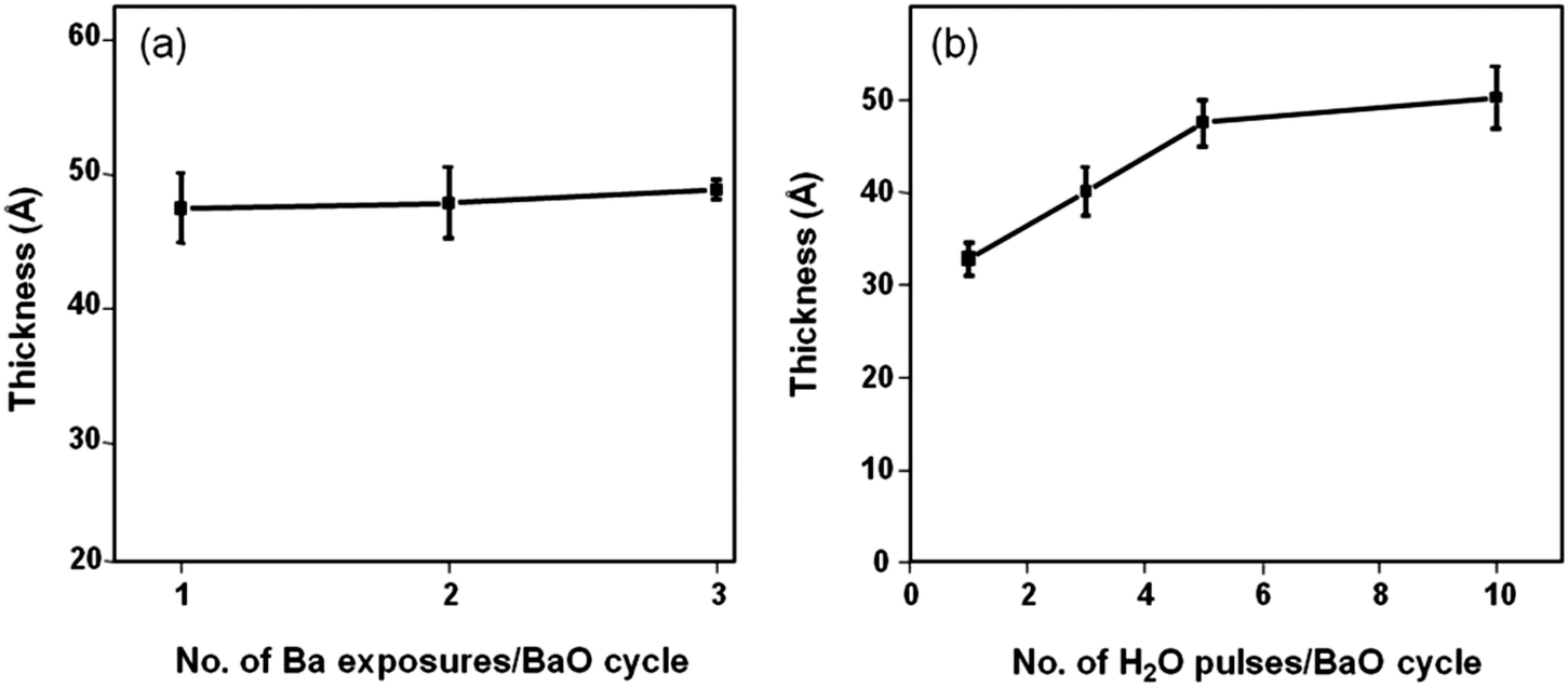 | ||
| Fig. 3 (a) Film thickness plotted versus number of Ba precursor exposures per BaO full cycle (b) thickness variation as a function of number of oxidant (H2O) pulses. A steady state was attained after 5–10 H2O pulses. 100 cycles were deposited in total. | ||
Having established the ALD window and self-limiting growth regime in both the half cycles, we checked the thickness uniformity on a four inch wafer. Fig. S3 (ESI†) shows a thickness map (ellipsometry) of the full wafer. X-ray reflectivity (XRR, ESI,† Fig. S5) validates the fitting. The direction of the precursor flow drives the overall thickness variation; however a std. dev. of 1.01 Å based on a 55-point measurement shows that this process offers excellent uniformity.
A precursor's suitability for ALD strongly correlates with the metal-to-ligand bond strengths.39 It should allow sufficient reactivity to the metal while preventing thermal decomposition as underlying reaction mechanism.40 Having experimentally established a self-limiting deposition regime for BaO with py-Ba, we now look into the dissociation energy differences between py-Ba and known cp-Ba (Table 1), known to easily thermally decompose.40
The energy to break both Ba–N bonds linking the metal to the ligands requires higher energy as compared to breaking the Ba–C bonds in cp-Ba. This is in line with the theoretical bond strengths of Ba–C (2.9 eV) and Ba–N (4.6 eV) calculated in the same way. The more stable Ba–N evidently prevents thermal decomposition of the precursor, which has been reported as a problem for the cp-type precursors with weaker bonding energies.40 Precluding any runaway growth, the higher dissociation energy may favor a surface controlled reaction at a lower growth rate and a deposition within the ALD window. The bond strength of the second pyrrole ligand to the metal center is higher for the first ligand. This agrees with the experiments in which several H2O pulses allow the reaction to proceed as also reported for other known metal-oxide ALD chemistries.41,42
B. Characterization of BaO films
X-ray photoelectron spectroscopy (XPS) depth profile reflects the overall quantitative Ba and O compositional uniformity (Fig. 4(a)).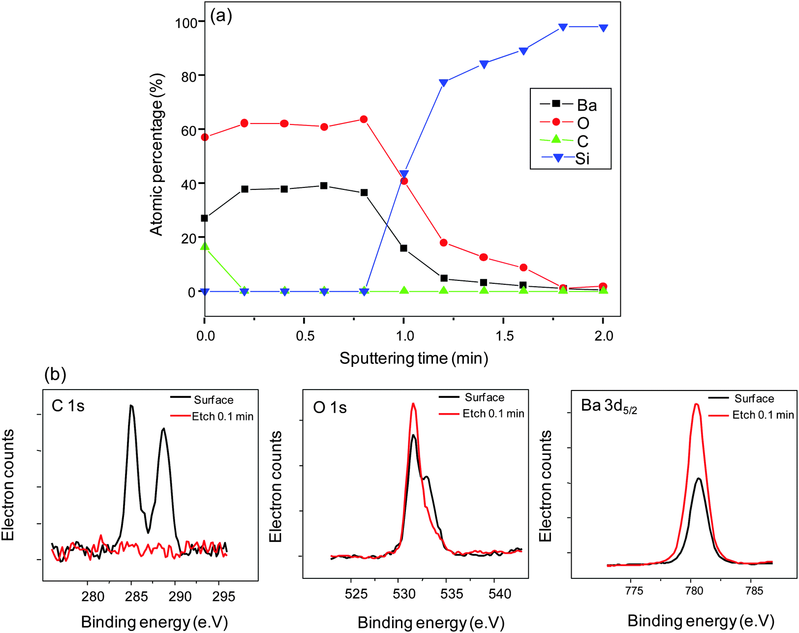 | ||
| Fig. 4 (a) XPS depth profile of BaO film obtained at 210 °C substrate temperature and 2 s boosting time. (b) C 1s, O 1s and Ba 3d5/2 X-ray photoelectron peaks on the surface of the film and post surface etching. | ||
BaO is not stable when exposed to air; it readily forms hydroxides/hydrates and/or carbonates.1 When transferring the samples to the XPS vacuum chamber after the film deposition, they were not in vacuum. Reactions between the as-deposited film and air cannot be ruled out. However, from the depth profile, the disappearance of the adventitious C 1s peak (285 eV)40 in the sputtered region of the film indicates the surface confinement of C (Fig. 4(b)). The peak at ∼290 eV shows BaCO3 formation on the surface43 eliminating possible bulk or molecular C inclusion from the precursor source. The O 1s core level spectra appear asymmetric on the surface of the film. The major component near the binding energy of 531.5 eV corresponds to bonding with Ba and the shoulder at 532.9 eV corresponds to Ba bonding with OH.25 The splitting in the O 1s peak is ∼1.5 eV. Reported values for O 1s splitting are ≤2 eV if associated to OH groups and ≥3 eV if associated to molecular H2O.44 Hence, the dominant feature at 532.9 eV corresponds to bonding to OH groups and not to H2O. The broad feature disappears after surface sputtering, leaving behind a single peak at 531.5 eV, which indicates that no OH species are present in the bulk of the film. This is further supported by the symmetric Ba 3d5/2 peak positioned at ∼780 eV indicating the single bonding environment around Ba in the entire film. We conclude the BaO deposition to be contamination free.
The BaO film deposited shows low surface roughness (root mean squared (RMS) roughness 2.1 Å) as analyzed by AFM (Fig. 5). In general, RMS-roughness values obtained were less than 5% of the film thickness.
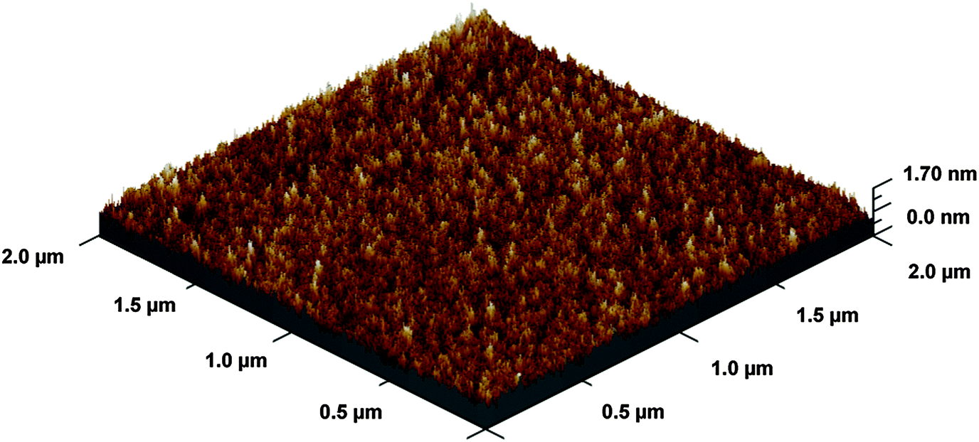 | ||
| Fig. 5 A 3D representation of BaO thin film grown at 210 °C. The film thickness is ∼4.5 nm and RMS roughness is ∼2.1 Å from AFM measurement. | ||
To investigate the conformality of film growth on non-planar substrates, ∼6.5–7 nm thick BaO was deposited onto a silicon substrate with vertical trenches. The trenches were 400 nm wide and 1 μm deep, corresponding to an aspect ratio of 1:2.5. Cross-sectional, HRTEM images of the interface area show their uniform coverage with ultrathin ALD BaO. Fig. 6(a) shows an overview of the trench. HRTEM images of its top, side and bottom interface are shown in Fig. 6(b–d). STEM-EELS line scans (Ba M4,5 and Si L2,3, ESI,† Fig. S7) reveal the BaO film thickness on the top (6.8 ± 1.5 nm, Fig. 6b), side (5.8 ± 0.6 nm, Fig. 6c) and bottom (6.55 ± 0.8 nm, Fig. 6d). This corresponds to a step coverage (thickness at the bottom/thickness at the top) of 91%.
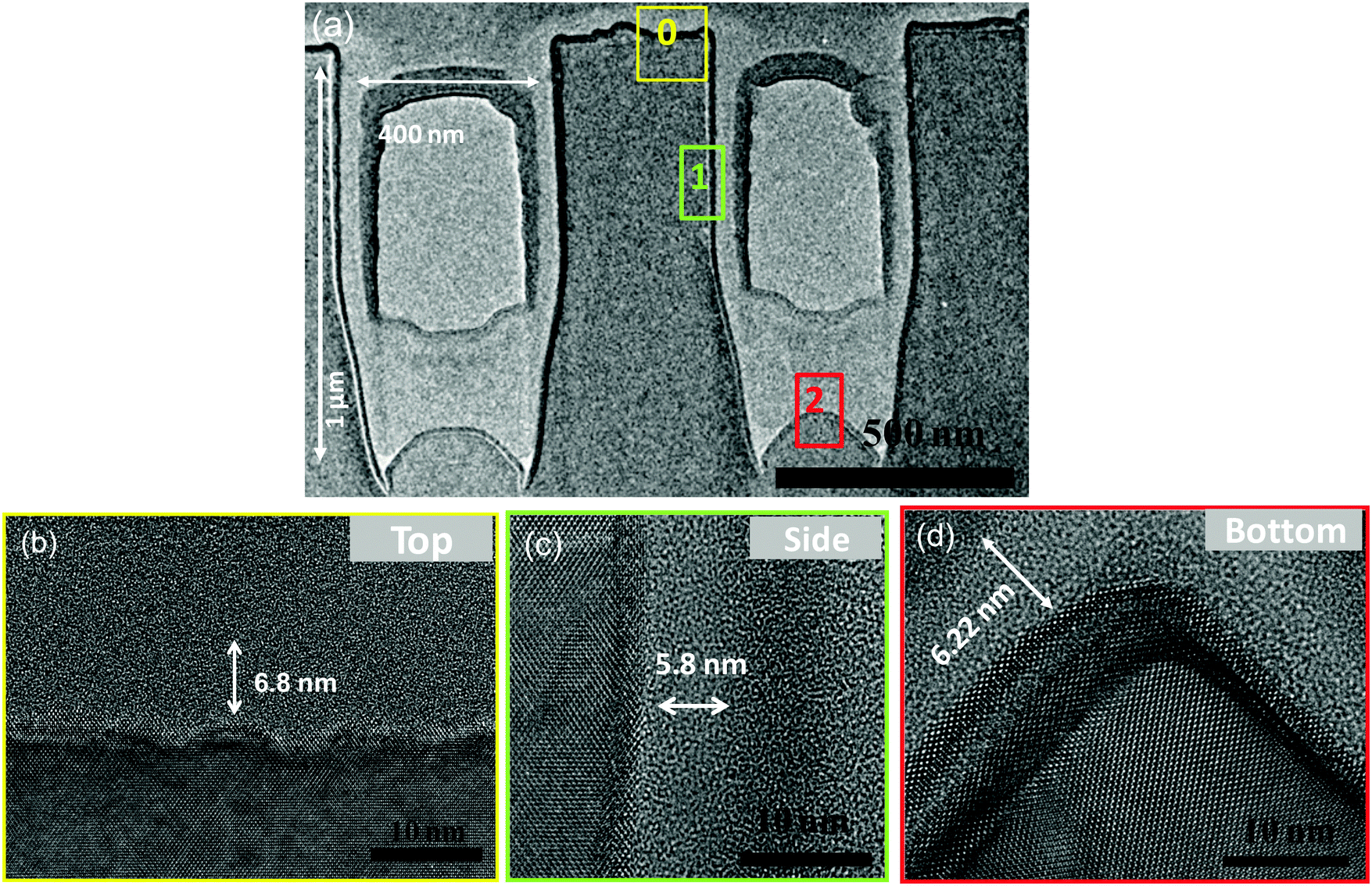 | ||
| Fig. 6 (a) Cross sectional TEM image of BaO film deposited on patterned Si substrate with aspect ratio ∼1:2.5; the central cavity of the trenches are filled with amorphous carbon for structure protection during ion milling; positions 0, 1 and 2 are highlighted as top, side and bottom of the trench, respectively. High resolution TEM of the positions 0, 1 and 2 are shown in (b), (c) and (d) respectively, white arrows show the thickness of BaO as obtained from STEM-EELS line scans (ESI,† Fig. S6). | ||
C. BTO deposition and electrical measurements
So far, we showed the successful deposition of self-limiting, ultrathin BaO films using py-Ba. Following known strategies for BTO deposition with cp-Ba,1,2,21 we grew films by alternating cycles of the binary oxides BaO and TiO2. BaO film deposition is described in section A. TiO2 deposition consisted of a TTIP dose (0.5 s) and an H2O dose (0.1 s) separated by a purging step (60 s) for each cycle. The substrate temperature was 210 °C.70 supercycles consisting of 4 BaO and 2 TiO2 cycles were deposited resulting in a stoichiometric composition of Ti/(Ba + Ti) = 0.53 (atomic percentage). Fig. 7a shows the uniform distribution of Ba and Ti atoms throughout the film. C contamination is surface confined indicating a low overall impurity level. The 1.6 eV shift to a lower binding energy of Ba 3d5/2 in the BTO ternary oxide film (ESI,† Fig. S8a) as compared to pure BaO evinces the formation of an intermixed BTO layer rather than sequential TiO2 and BaO layers. As reported elsewhere,1 ALD BTO films are generally amorphous after deposition. Selected-area TEM diffraction (SAD) pattern in ESI,† Fig. S9 shows absence of any diffraction rings supporting that our films are largely amorphous. Cross sectional TEM images reveal the morphology of the films. Fig. 7a shows the smooth surface, uniform thickness (∼7 nm) over a large area and the absence of phase separation.
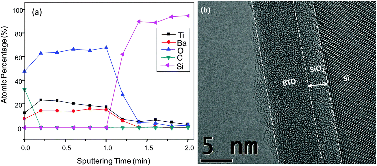 | ||
| Fig. 7 (a) XPS Depth profile of as deposited BTO grown on Si substrate at 210 °C. (b) High resolution cross sectional TEM image of ∼7 nm thick BTO film with stoichiometry at Ti/(Ba + Ti) = 0.53 (Ba:Ti ∼ 1:1) on a Si substrate with an interfacial oxide thickness of ∼2 nm. | ||
To show the potential of py-Ba for fabricating high-k dielectric devices, we fabricated an MIM architecture (Pt/BTO/RuO2/Ru) with a ∼20 nm thick BTO film (200 supercycles). We measured a capacitance (C) of 7.2 nF at 1 kHz and 0 V (effective zero bias, ESI,† Fig. S10), extracting a dielectric constant (εBTO) of 35 (using the formula C = εBTO × ε0 × A/tBTO, where A is the electrode area and tBTO is the film thickness). This resulted in an equivalent oxide thickness (EOT) of 2.2 nm (tBTO × (εSiO2/εBTO)), where εSiO2 is the dielectric constant of SiO2. Our as-deposited film outperforms existing BTO MIM film devices.1,45,46 Compared to sputtered films, the improved dielectric performance was likely due to ALD's advantage in continuity, conformality, and obtainable feature sizes.46,47 The improvement over existing ALD BTO1 MIM devices hints towards the formation of non-detected crystallites in their dominant amorphous surrounding.1,21,48 This might have evolved through one or several of the following factors: (a) thermal annealing of the BTO film due to local heating underneath the Pt top electrode during its evaporation, (b) the BTO's deposition on a Ru substrate potentially enabling the growth of small crystallites and/or (c) long exposure to elevated temperatures during the long depositions that involved extended purge and pump steps as well as several oxidant pulses (see Experimental).
The BTO device reported here, shows a typical45,49 non-linear current–voltage (I–V) characteristic as shown in Fig. 8. At low voltages, we observed a sudden increase of current followed by an exponential increase at higher voltages. Despite the thinness of the film, it exhibits a very low leakage current density of only 10−8 A cm−2 at 1.6 V. Capacitance–voltage (C–V) measured at 1 kHz (ESI,† Fig. S10) shows no C–V hysteresis, indicating the absence of any remanent polarization in the reported MIM device. This is very likely due to the dominating amorphous nature of the film.1,49,50
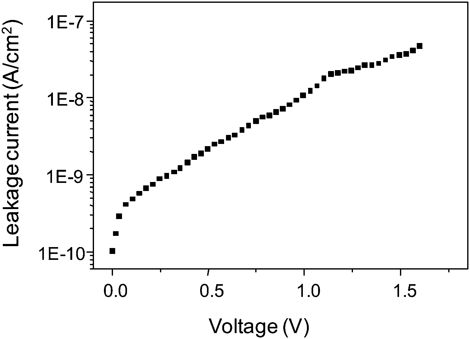 | ||
| Fig. 8 Representative leakage current (I–V) characteristics of Pt/BTO/Ru capacitor measured for a 20 nm thick BTO layer. The top electrode defines the capacitor area (0.68 × 10⁻³)2 m2. | ||
Conclusion
A new pyrrole based precursor (py-Ba) enabled the first self-limiting ALD growth of BaO. Using H2O as oxidant, we have reported the lowest BaO deposition temperature thus far (180–210 °C) at a GPC of 0.45 Å per cycle on Si substrates. The deposited films show high purity, compositional uniformity, smooth surface and conformality on non-planar substrates. As a proof-of-concept for depositing multicomponent BaO containing films, BTO was grown intermixing BaO with TiO2 (TTIP as Ti precursor and H2O as oxidant). Promising electrical properties on an MIM structure have been reported for as-deposited amorphous BTO films. The results show that self-limiting BaO deposition using py-Ba as precursor allows exploiting the properties of BaO containing multinary materials in the ultrathin regime. In applications requiring precise thickness and stoichiometry control, conformal coverage over large areas and on complex shaped substrates, low roughness and low deposition temperatures, py-Ba will likely play a role in future ALD processes involving BaO.Acknowledgements
This work was funded by BASF SE (Ludwigshafen, Germany). SA and JT have contributed equally to the work. The authors thank BASF for the very fruitful collaboration that has made this project possible. The authors thank SNSF and SNF shared facilities at Stanford for characterization of the films. Furthermore, JT acknowledges the financial support of the Austrian Science Fund (FWF) under the contract J3505-N20. The authors thank Dr. James Palko and Yonas Yemane from Stanford University for their valuable inputs and for proof-reading.References
- M. Vehkamäki, T. Hatanpää, M. Ritala, M. Leskelä and S. Väand E. Rauhala, Chem. Vap. Deposition, 2007, 13, 239–246 CrossRef.
- M. Vehkamäki, T. Hatanpää, T. Hänninen, M. Ritala and M. Leskelä, Electrochem. Solid-State Lett., 1999, 2, 504–506 CrossRef.
- M. W. Cole, E. Ngo, C. Hubbard, S. G. Hirsch, M. Ivill, W. L. Sarney, J. Zhang and S. P. Alpay, J. Appl. Phys., 2013, 114, 164107 CrossRef.
- J. H. Shim, J. S. Park, J. An, T. M. Gür, S. Kang and F. B. Prinz, Chem. Mater., 2009, 21, 3290–3296 CrossRef CAS.
- Y. Yamazaki, R. Hernandez-Sanchez and S. M. Haile, Chem. Mater., 2009, 21, 2755–2762 CrossRef.
- B. Jaffe, Piezoelectric Ceramics, Elsevier, 2012 Search PubMed.
- J. G. Bednorz and K. A. Müller, Z. Phys. B: Condens. Matter, 1986, 64, 189–193 CrossRef CAS.
- M. R. Norman, Nat. Phys., 2013, 9, 757–758 CrossRef CAS.
- L. Zhang, Y. Shi, S. Peng, J. Liang, Z. Tao and J. Chen, J. Photochem. Photobiol., A, 2008, 197, 260–265 CrossRef CAS.
- K. Meng, P. K. Surolia and K. R. Thampi, J. Mater. Chem. A, 2014, 2, 10231 CAS.
- S. Liu, H. Zhang, L. Sviridov, L. Huang, X. Liu, J. Samson, D. Akins, J. Li and S. O’Brien, J. Mater. Chem., 2012, 22, 21862 RSC.
- G. Rijnders and D. H. A. Blank, Nature, 2005, 433, 369–370 CrossRef CAS PubMed.
- H. N. Lee, H. M. Christen, M. F. Chisholm, C. M. Rouleau and D. H. Lowndes, Nature, 2005, 433, 395–399 CrossRef CAS PubMed.
- S. M. George, Chem. Rev., 2010, 110, 111–131 CrossRef CAS PubMed.
- R. W. Johnson, A. Hultqvist and S. F. Bent, Mater. Today, 2014, 17, 236–246 CrossRef CAS.
- X. Jiang, H. Huang, F. B. Prinz and S. F. Bent, Chem. Mater., 2008, 20, 3897–3905 CrossRef CAS.
- P. Schindler, M. Logar, J. Provine and F. B. Prinz, Langmuir, 2015, 31, 5057–5062 CrossRef CAS PubMed.
- A. A. Dameron, S. D. Davidson, B. B. Burton, P. F. Carcia, R. S. McLean and S. M. George, J. Phys. Chem. C, 2008, 112, 4573–4580 CAS.
- E. Graugnard, O. M. Roche, S. N. Dunham, J. S. King, D. N. Sharp, R. G. Denning, A. J. Turberfield and C. J. Summers, Appl. Phys. Lett., 2009, 94, 263109 CrossRef.
- T. Hatanpää, M. Vehkamäki, I. Mutikainen, J. Kansikas, M. Ritala and M. Leskelä, Dalton Trans., 2004, 1181–1188 RSC.
- J. An, T. Usui, M. Logar, J. Park, D. Thian, S. Kim, K. Kim and F. B. Prinz, ACS Appl. Mater. Interfaces, 2014, 6, 10656–10660 CAS.
- R. Schafranek, A. Giere, A. G. Balogh, T. Enz, Y. Zheng, P. Scheele, R. Jakoby and A. Klein, J. Eur. Ceram. Soc., 2009, 29, 1433–1442 CrossRef CAS.
- B. Chen, H. Yang, L. Zhao, J. Miao, B. Xu, X. G. Qiu, B. R. Zhao, X. Y. Qi and X. F. Duan, Appl. Phys. Lett., 2004, 84, 583–585 CrossRef CAS.
- W. Lee, J. H. Han, W. Jeon, Y. W. Yoo, S. W. Lee, S. K. Kim, C.-H. Ko, C. Lansalot-Matras and C. S. Hwang, Chem. Mater., 2013, 25, 953–961 CrossRef CAS.
- S. K. Kim, G.-J. Choi, S. Y. Lee, M. Seo, S. W. Lee, J. H. Han, H.-S. Ahn, S. Han and C. S. Hwang, Adv. Mater., 2008, 20, 1429–1435 CrossRef CAS.
- H. Tsuchiya, J. M. Macak, L. Taveira and P. Schmuki, Chem. Phys. Lett., 2005, 410, 188–191 CrossRef CAS.
- S. K. Kim, S. W. Lee, J. H. Han, B. Lee, S. Han and C. S. Hwang, Adv. Funct. Mater., 2010, 20, 2989–3003 CrossRef CAS.
- A. W. Ott, J. W. Klaus, J. M. Johnson and S. M. George, Thin Solid Films, 1997, 292, 135–144 CrossRef CAS.
- A. K. Rappe, C. J. Casewit, K. S. Colwell, W. A. Goddard III and W. M. Skiff, J. Am. Chem. Soc., 1992, 114, 10024–10035 CrossRef.
- C. Lee, W. Yang and R. G. Parr, Phys. Rev. B: Condens. Matter Mater. Phys., 1988, 37, 785–789 CrossRef.
- A. D. Becke, Phys. Rev. A: At., Mol., Opt. Phys., 1988, 38, 3098–3100 CrossRef.
- M. J. Frisch, G. W. Trucks, H. B. Schlegel, G. E. Scuseria, M. A. Robb, J. R. Cheeseman, G. Scalmani, V. Barone, B. Mennucci, G. A. Petersson, H. Nakatsuji, M. Caricato, H. P. Hratchian, A. F. Izmaylov, J. Bloino, G. Zheng, J. L. Sonnenberg, M. Hada, M. Ehara, K. Toyota, R. Fukuda, J. Hasegawa, M. Ishida, T. Nakajima, Y. Honda, O. Kitao, H. Nakai, T. Vreven, J. A. Montgomery, J. E. Peralta, F. Ogliaro, M. Bearpark, J. J. Heyd, E. Brothers, K. N. Kudin, V. N. Staroverov, R. Kobayashi, J. Normand, K. Raghavachari, A. Rendell, J. C. Burant, S. S. Iyengar, J. Tomasi, M. Cossi, N. Rega, J. M. Millam, M. Klene, J. E. Knox, J. B. Cross, V. Bakken, C. Adamo, J. Jaramillo, R. Gomperts, R. E. Statmann, O. Yazyev, A. J. Austin, R. Cammi, C. Pomelli, J. W. Ochterski, R. L. Martin, K. Morokuma, V. G. Zarkzewski, G. A. Voth, P. Salvador, J. J. Dannenberg, S. Dapprich, A. D. Daniels, O. Farkas, J. B. Foresman, J. V. Ortiz, J. Cioslowski and D. J. Fox, Gaussian, 2010 Search PubMed.
- W. R. Wadt and P. J. Hay, J. Chem. Phys., 1985, 82, 284 CrossRef CAS.
- A. K. Wilson, T. van Mourik and T. H. Dunning Jr., THEOCHEM, 1996, 388, 339–349 CrossRef.
- G. Liu, A. Bertuch, M. Sowa, Ritwik Bhatia, E. Deguns, M. Dalberth, G. Sundaram and J. S. Becker, Method and apparatus for precursor delivery, US Pat., US 20110311726 A1, 2011 Search PubMed.
- R. L. Puurunen, J. Appl. Phys., 2005, 97, 121301 CrossRef.
- H. Wang, X. Jiang and B. G. Willis, J. Vac. Sci. Technol., A, 2012, 30, 01A133 Search PubMed.
- R. Hummatov, O. Gülseren, E. Ozensoy, D. Toffoli and H. Üstünel, J. Phys. Chem. C, 2012, 116, 6191–6199 CAS.
- T. P. Holme and F. B. Prinz, J. Phys. Chem. A, 2007, 111, 8147–8151 CrossRef CAS PubMed.
- W. Lee, J. H. Han, W. Jeon, Y. W. Yoo, S. W. Lee, S. K. Kim, C.-H. Ko, C. Lansalot-Matras and C. S. Hwang, Chem. Mater., 2013, 25, 953–961 CrossRef CAS.
- M. J. Kelly, J. H. Han, C. B. Musgrave and G. N. Parsons, Chem. Mater., 2005, 17, 5305–5314 CrossRef CAS.
- M. Reinke, Y. Kuzminykh and P. Hoffmann, Chem. Mater., 2015, 27, 1604–1611 CrossRef CAS.
- M. Wegmann, L. Watson and A. Hendry, J. Am. Ceram. Soc., 2004, 87, 371–377 CrossRef CAS.
- V. M. Fuenzalida, M. E. Pilleux and I. Eisele, Vacuum, 1999, 55, 81–83 CrossRef CAS.
- K. Sreenivas, A. Mansingh and M. Sayer, J. Appl. Phys., 1987, 62, 4475–4481 CrossRef CAS.
- P. Li, T.-M. Lu and H. Bakhru, Appl. Phys. Lett., 1991, 58, 2639–2641 CrossRef CAS.
- Z. Li, A. Rahtu and R. G. Gordon, J. Electrochem. Soc., 2006, 153, C787 CrossRef CAS.
- P. Schindler, Y. Kim, D. Thian, J. An and F. B. Prinz, Scr. Mater., 2016, 111, 106–109 CrossRef CAS.
- E. K. Evangelou, N. Konofaos and C. B. Th, Philos. Mag. B, 2000, 80, 395–407 CrossRef CAS.
- V. R. Chinchamalatpure, S. A. Ghosh and G. N. Chaudhari, Mater. Sci. Appl., 2010, 01, 187–190 CAS.
Footnotes |
| † Electronic supplementary information (ESI) available: Supporting figures including TGA, XRR, STEM-EELS, XPS, SAD, and C–V plots. See DOI: 10.1039/c5tc03561a |
| ‡ These authors contributed equally to the work. |
| This journal is © The Royal Society of Chemistry 2016 |