Studies into the Yb-doping effects on photoelectrochemical properties of WO3 photocatalysts†
Siao Li Liew*,
Gomathy Sandhya Subramanian,
Chin Seng Chua and
He-Kuan Luo*
Institute of Materials Research and Engineering, Agency for Science, Technology and Research, 2 Fusionopolis Way, #08-03, Innovis, Singapore 138634. E-mail: sl-liew@imre.a-star.edu.sg; luoh@imre.a-star.edu.sg
First published on 5th February 2016
Abstract
Yb-doped WO3 photocatalysts were prepared by co-sputtering Yb and WO3 on FTO glass and then sintering at elevated temperatures in air. At sintering temperatures between 450 and 550 °C, the photocurrent densities of Yb-doped WO3 photocatalysts were higher and more stable than those of pristine WO3 photocatalysts. The Yb-doping effects on the photoelectrochemical properties were investigated using Raman, transient absorption and electrochemical impedance spectroscopies. Compared to pristine WO3 photocatalysts, Yb-doped photocatalysts sintered at up to 550 °C consist of sub-stoichiometric WO3−x due to the substitution of W6+ cations with Yb3+ dopants, displaying shorter electron–hole recombination times and higher levels of donor densities.
Introduction
Tungsten trioxide (WO3) finds many applications as photocatalysts and gas sensors owing to its intrinsic properties of visible light-responsive band gap, free carrier diffusion length and good chemical stability in aqueous media. Over the years, much effort has been made to incorporate another metal into the semiconducting metal oxide to further enhance its photoelectrochemical properties. For example, the catalytic modification of a WO3 surface via the electrodeposition of Pt particles could promote the reaction rate of methanol oxidation at the photoanode, leading to a significantly enhanced H2 production efficiency, compared with when using unmodified WO3.1 It has also been reported that Pt-modified WO3 films can be used as H2 sensors which exhibit lower electrical resistances at higher Pt concentrations, favouring H2 detection possibly due to the catalytic effects of Pt clusters on the dissociative adsorption of H2 to form H-atoms. This catalytic dissociative effect releases electrons into the WO3 matrix which in turn decreases the electrical resistance.2 Pt nanoparticles can also be loaded onto nanoporous WO3 nanotubes, which greatly increases photocatalytic activity because the large surface area of WO3 nanotubes offers many more active sites in close proximity to the Pt nanoparticles to facilitate the transfer of photoelectrons to the Pt nanoparticles.3To enhance the photoelectrochemical properties of WO3, the incorporation of other transition metals such as Mo, Ti and Fe has also been investigated.4–6 In MoxW1−xO3 hydrates, Mo6+ ions were preferred to W6+ ions as trapping sites for electrons.4 Therefore the substitution of W6+ with Mo6+ cations led to a red shift in the absorption edge due to the reduction of Mo6+ to Mo5+. Hence the photoelectrochemical response of WO3 photoanodes to visible light was enhanced together with the red shift. Doping of Ti4+ into a WO3 semiconductor also improved the photocatalytic performance under visible light due to the change in the band structure of WO3 caused by impurity states between the conduction band and valence band resulting in a narrower band gap.5 The modification of a WO3 surface with Fe3+ extended the absorption region and reduced the charge transfer resistance, leading to an increased photocurrent density.6 All of these dopings of transition metals had the common effect of narrowing the band gap of WO3 and extending the absorption to the visible region of the solar spectrum.
A different mechanism that proceeds through harnessing the electron-rich f-orbitals of Yb dopants in WO3 was reported for the first time in our earlier study.7 We prepared and investigated Yb-doped WO3 photocatalysts of varying Yb concentrations for photoelectrochemical water splitting. For a Yb doping concentration as low as 0.34 at%, determined by X-ray photoelectron spectroscopy, an evident enhancement in the photocurrent density was observed, which was attributed to an increase in conductive carrier paths caused by oxygen vacancies and the 4f13 orbital configuration of the Yb3+ doped into the WO3. However, a higher doping concentration of 1.6 at% increased the charge transfer resistance and reduced the photocurrent density compared to pristine WO3, possibly due to a distortion of the WO3 crystal structure induced by the larger ionic radius of Yb3+ relative to W6+. Notwithstanding the limiting factor of the size of Yb3+ dopant cations, the study showed that tapping into the electron-rich f-orbitals of the lanthanide proved to be an effective means to increase charge carrier generation for enhanced photocurrent densities in WO3.
In order to obtain a deeper and better understanding of Yb-doped WO3 photocatalysts for practical applications, herein we have studied the effects of Yb-doping, at varying sintering temperatures, on the photoelectrochemical properties of the material. The results showed that Yb doping enlarged the thermal envelope of WO3. Specifically, photocurrent densities of Yb-doped WO3 were sustained up to 550 °C. However for pristine WO3 photocatalysts, the photocurrent density continually decreased with an increasing sintering temperature over the same range. These improvements were evaluated in the light of structural properties, charge dynamics and donor densities of thermally treated photocatalysts investigated with Raman, transient absorption and electrochemical impedance spectroscopies. The Yb-doped WO3 photocatalysts sintered at up to 550 °C were sub-stoichiometric due to the substitution of W6+ with Yb3+ dopants and showed a shorter electron–hole recombination time but higher donor densities compared to pristine WO3 photocatalysts. Yb-doping led to more stable and higher photocurrent densities with lower charge transfer resistances for PEC water splitting with the Yb-doped WO3 photocatalysts.
Experimental details
Deposition
WO3 and Yb were co-sputtered onto ultrasonically cleaned FTO glass substrates inside a magnetron sputtering chamber when the base pressure reached ∼10−7 Torr. The sputtering power was set at 100 W and 5 W for WO3 and Yb, respectively, in order to yield as-deposited film thicknesses of ∼450 nm. The sputtered samples were sintered in air in a box furnace in a temperature range between 400 and 600 °C for 1 hour. A set of pristine WO3 samples (without Yb) was also prepared using the same process parameters.Characterisations
Structural analyses were carried out with a WITec alpha 300R microscope system using a 532 nm Nd YAG laser of ∼1 mW power to obtain Raman spectra of the samples. The spectroscopy for each sample was averaged at 1 μm per pixel and 0.1 s per point from a 100 × 100 μm scan area at a 100× objective. Transient absorption spectroscopy was carried out using a Nd:YAG laser (1 mJ, 7 ns, 10 Hz, 355 nm excitation) as the pump source and a 450 W xenon arc lamp as the probe source. Each spectral curve is the average of 256 measurements while each kinetics decay curve is the average of four measurements at 16 laser shots per measurement. Secondary ion mass spectroscopy (SIMS) using ION SIMS IV to profile the distribution of Yb in WO3 and optical absorbance measured with a Shimadzu UV-3101 PC scanning spectrophotometer were carried out to supplement the spectroscopic results.Photoelectrochemical (PEC) measurements and detection of gases (H2 and O2)
PEC measurements were carried out in a custom-made two-compartment glass cell with a three-electrode configuration. A Pt wire as the counter electrode was placed in one compartment, separated from a Ag/AgCl reference electrode and the working electrode (sputter-deposited WO3 on FTO substrate) in another compartment. 400 mL of Na2SO4 (0.05 M, pH ∼ 5.4) electrolyte solution, which had already been purged with Ar, was added to the glass cell. Current–voltage measurements under dark and illuminated conditions at a scan rate of 100 mV s−1 between −0.1 and 1.6 V Ag/AgCl were controlled using a potentiostat (Autolab PGSTAT101) connected to Nova 1.8 software. For the illuminated measurements, a xenon light source (Hamamastu LC8) with a radiant spectrum that resembles the visible portion of the solar spectrum was directed at the working electrode through a quartz window in the PEC glass cell. The intensity of the light had already been adjusted to 100 mW cm−2 based on the output reading of a calibrated Si solar cell. The illuminated area on the working electrode was measured to be ∼1.5 cm by 1.0 cm. Electrochemical impedance spectroscopy was also performed using the same test cell set-up to obtain Nyquist and Mott–Schottky plots to determine the charge transfer resistance and donor density respectively. For the Nyquist plots, the cell was illuminated and maintained at constant bias voltages superimposed with a sinusoidal voltage of 10 mV in a frequency range between 0.1 Hz and 10 kHz. For the Mott–Schottky plots, measurements were made in the dark at selected frequencies between bias voltages of −0.2 and 1.3 V Ag/AgCl.A custom-built photocatalytic reactor comprising a photoelectrochemical cell and a gas chromatograph was used to simultaneously measure photocurrents and quantify gaseous products from water splitting. The cell was an 820 cm3 glass vessel configured with a two-electrode set-up consisting of a Pt counter electrode and the sputter-deposited WO3 working electrode. During the photoelectrochemical measurements, the WO3 photocatalyst inside the cell was illuminated at a light intensity of 50 mW cm−2 using a 150 W xenon arc lamp fitted with an AM1.5 filter. A constant 1.5 V bias voltage was applied through a potentiostat to the counter electrode during the measurements. ∼220 mL of the same electrolyte as was used in the previous section was used in this test. The gases from the photoelectrochemical cell were delivered by a high purity Ar carrier gas to a gas chromatograph (GC-2014 Shimadzu) for analysis.
Results and discussion
Structural analyses
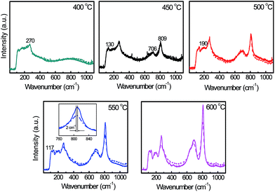
At a sintering temperature of 400 °C, both the Yb-doped and pristine WO3 samples displayed broad Raman spectra with a weak band region around a wavenumber of 200 cm−1 and a peak at 270 cm−1, as shown in Fig. 1. This band region evolved into peaks at 130, 190 and 117 cm−1 and new peaks appeared at 706 and 809 cm−1 when the sintering temperature was increased to 450 °C and beyond. All of the peaks which increased in intensity and sharpness with increasing sintering temperature, clearly identified both the Yb-doped and pristine photocatalysts as monoclinic WO3 with peaks at the 200 cm−1 band region ascribed to lattice vibration, 270 cm−1 to bending and 706–809 cm−1 to stretching vibrations of W–O bonds in monoclinic WO3.8,9 At sintering temperatures of 500 °C and above, Raman peaks of the Yb-doped WO3 appeared weaker than those of its pristine counterpart with clear differences observed at 550 and 600 °C in all of the peak regions. In addition, Yb-doping also caused a minor shift of ∼2 cm−1 to lower bond energies as shown in the inset graph which indicates a less ordered crystal lattice in the Yb-doped WO3 compared to the pristine WO3.Distribution of Yb
Elemental depth profiling of Yb-doped WO3 samples with SIMS (see Fig. S1a†) showed that Yb distribution followed those of W and O, indicating that Yb was uniformly incorporated into the WO3 lattice. The average composition of the Yb-doped samples was WYb0.025O3−x from elemental analyses using an Oxford INCA X-ray energy dispersive spectrometer (EDS). The Raman and SIMS results in combination showed that it is very likely that the Yb3+ dopants substituted W6+ in the crystal lattice to form sub-stoichiometric WO3−x which would be less crystalline than pristine WO3.10 This is in agreement with the colour change from pale green in the pristine WO3 to deep blue in the Yb-doped WO3 as displayed by the samples shown in Fig. S1b.†Carrier lifetime
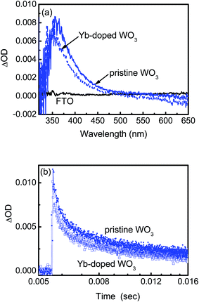
The effect of Yb-doping on carrier transport was probed using transient absorption (TA) spectroscopic measurements. Fig. 2a shows the TA spectra obtained in the spectral range between 300 and 650 nm for the WO3 photocatalysts and FTO substrate, recorded after a 100 ns delay upon excitation by a 355 nm laser. Strong TA signals with maxima (in the ∼352 to 357 nm region) were registered for both Yb-doped and pristine WO3 with Yb-doped WO3 exhibiting a lower signal level and a blue shift relative to pristine WO3. TA spectra with maxima in the UV-visible region have been ascribed to absorption by photoholes in metal oxides such as Fe2O3, WO3, TiO2 and BiVO4.11–14 A lower TA signal for Yb-doped WO3 would imply that fewer photoholes were probed in the spectral range possibly due to faster recombination of electrons and holes in the less ordered crystal lattice. The blue shift observation corroborates with the optical absorption spectra in Fig. S2† which show that Yb doping did not produce the desired red shifts in the absorption edges of WO3 for all of the sintering temperatures, unlike for the reported doping effects of Mo, Ti and Fe transition metals into a WO3 semiconductor where the band gap was narrowed and the absorption region was extended to the visible range of the solar spectrum (i.e. red shift).4–6 Both the TA and optical absorption spectra in this present study suggested that the presence of Yb oxides with wide band gaps in the Yb-doped WO3 probably contributed to the non-red shifts in the absorption edges. Fig. 2b shows the decay kinetics of TA probed at a 400 nm wavelength, which revealed a rapid decrease in the TA signals for the first 10 ms followed by a gradual decrease for up to 0.1 s for both the Yb-doped and pristine photocatalysts, which resembles the occurrence of bulk recombination of electrons and holes in semiconductor photocatalysts in similar excitation conditions.11,13,15 However the reported recombination times t1/2 (time to reach half of the initial concentration of charge carriers) of these photocatalysts were usually in the order of microseconds. In the present study with no bias voltage applied, the t1/2 values for both the Yb-doped and pristine WO3 samples were higher than the literature values11,13,15 with the Yb-doped WO3 having a shorter t1/2 of ∼0.46 ms compared to 0.87 ms for the pristine WO3. t1/2 of the Yb-doped WO3 shows that the mobility of free carriers in the doped photocatalyst was not severely impaired by the doping with Yb even though Raman spectroscopic measurements indicated that the crystal lattice was less ordered in the Yb-doped WO3 compared to the pristine WO3. The long recombination time in WO3 is linked to its free carrier diffusion length which can be up to two orders of magnitude higher than that of either TiO2 or Fe2O3. A long carrier lifetime is desired in photocatalytic applications for increased free electron–hole pairs to enhance photocurrents although it does not necessarily lead to increased photocurrents.Photoelectrochemical (PEC) studies
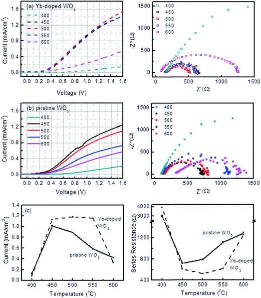
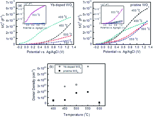
The photocurrent densities and electrochemical impedances from the PEC testing are plotted in Fig. 3. Between the sintering temperatures of 450 and 550 °C, the photocurrent densities of Yb-doped WO3 photocatalysts were both fairly constant and higher than for pristine WO3. However, the photocurrents of Yb-doped WO3 photocatalysts sintered at 400 and 600 °C were low. The charge transfer resistance values corresponded to the photocurrent densities albeit in an opposite trend. Fig. 3c summarises the contrasting effects of the sintering temperature from 450 to 550 °C (at 1.2 V Ag/AgCl) for Yb-doped WO3 which maintained a constant level of 1.2 mA cm−2 (corresponding to 525 to 626 Ω) and for pristine WO3 which displayed a decreasing level from 1.0 to 0.4 mA cm−2 (corresponding to 710 to 1300 Ω).To further investigate the effects of Yb-doping on photocurrents, electrochemical impedance spectroscopy (EIS) measurements for each photocatalyst were carried out in the dark at 1000 Hz between −0.2 and 1.4 V to obtain capacitance values which were fitted to the Mott–Schottky (MS) equation as shown in Fig. 4. Except for samples sintered at 400 and 600 °C, the slope of each MS plot, which is equal to  , was significantly lower for Yb-doped WO3 compared to pristine WO3, in other words doping resulted in increased donor densities (note: e is the electron charge, ε is the dielectric constant of WO3 (50), εo is vacuum permittivity, and ND is donor density).16 As Yb was co-sputtered at the same sputtering power for all of the doped samples, it is expected that ND will be similar for all of the doped samples regardless of the sintering temperature. As shown in Fig. 4b, the ND values ranged from 2.92 × 10²⁰ to 6.33 × 1020 cm−3 for Yb-doped WO3 versus a lower level of 6.08 × 10¹⁹ to 1.98 × 1020 cm−3 for pristine WO3 for sintering temperatures between 450 and 550 °C. The ND values for both doped and pristine WO3 were however low at the extreme temperatures (400 and 600 °C) when compared to the respective ND values for the 450 to 550 °C range.
Thus far, it has been shown that Yb-doped WO3 photocatalysts demonstrated photocurrent enhancement with reduced charge transfer resistances. Raman spectroscopy and SIMS results (Fig. 1 and S1†) showed that Yb3+ dopants substituted W6+ in the crystal lattice which would have resulted in oxygen vacancies to form sub-stoichiometric WO3−x. Oxygen vacancies created in PO4 salts have been reported to widen the valence band and thus narrow the band gap to yield enhanced photoactivity.17,18 However in the present study, a blue shift (hence there is no narrowing of the band gap) was observed in the transient absorption spectra instead (Fig. 2) which more probably reflects the presence of Yb oxides with wide band gaps. Besides, the carrier life time of Yb-doped WO3 was shorter than that of pristine WO3. The enhanced photocatalytic activity of Yb-doped WO3 is attributed to increased donor densities as shown in the Mott–Schottky plots in Fig. 4. The electrons available from the 4f and 6s orbitals of Yb and the shallow electron donors from the oxygen vacancies19 arising from the substitution of W by Yb contributed to a higher electron density for the doped WO3. Even at increased sintering temperatures where an amorphous layer formed at the WO3/electrolyte interface would thicken,20 the higher electron density would enable more free electrons to tunnel through to result in reduced charge transfer resistances and hence increased photocurrent densities. The higher electron density effect was sustained to sintering temperature of up to 550 °C as indicated by the stabilities of the photocurrent densities and the electrochemical impedances of the Yb-doped WO3, as shown in Fig. 3c. In contrast, a lower electron density in the pristine WO3 would be impeded by the amorphous layer formed at the WO3/electrolyte interface and led to decreasing photocurrents and increasing electrochemical impedances over the same sintering temperature range. However at the extreme sintering temperatures of 400 and 600 °C, the photocurrent densities of both the Yb-doped and pristine WO3 were lower as shown in Fig. 3c, which corresponds to the decreased electron density levels shown in Fig. 4. At 400 °C, both the doped and pristine WO3 were not fully crystallised, as indicated by the broad Raman spectra for 400 °C in Fig. 1, which implies the presence of grain boundaries to trap free electrons. On the other hand at 600 °C, although the crystallinities of both the doped and pristine WO3 increased, as shown by the sharp peaks in the Raman spectra for 600 °C in Fig. 1, the amorphous layer formed at the photocatalyst/electrolyte interface by oxidation20 could have altered the effective dielectric constants of the photocatalysts and lowered the capacitance values and the free donor carrier densities. While the present study shows that doping a small amount of electron-rich Yb can increase donor densities and lead to higher PEC photocurrent densities, increasing the doping level of Yb in WO3 continuously may nullify the benefits of increasing donor density due to the distortion of the WO3 crystal structure which impedes charge transport and increases charge transfer resistance, as reported in our earlier study.7
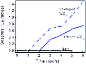
To confirm that the photocurrents of the Yb-doped and pristine WO3 photocatalysts sputter-deposited in this study were due to photoelectrochemical reaction of water, the water splitting products (H2 and O2) were collected and analysed using the in-house photocatalytic reactor coupled with a gas chromatograph. H2 gas was detected at hourly intervals as shown in the gas evolution plot in Fig. 5; however O2 gas was not so conclusively identified during the first half of the reaction (∼3 hours), which was probably due to the lower amount being produced and its higher solubility in water. Electrolysis in the dark with the same photocatalyst was also carried out to verify that no gaseous products were collected without light irradiation. 1.46 μmol of H2 had been collected at the end of six hours of the photocatalytic reaction using Yb-doped WO3. Given that the surface area of the photocatalyst was 1.5 × 1.0 cm2, the H2 yield was ∼2000 μmol h−1 m−2 which is considerably lower than those reported for WO3 nanostructures.21–23 Yet high photo-stability was demonstrated with only an ∼10% drop in the photocurrent at the end of 6 hours of photocatalysis, as shown in Fig. S3.†
Conclusions
We prepared Yb-doped WO3 photocatalysts via the co-sputtering of Yb and WO3, followed by sintering at elevated temperatures in air from 400 to 600 °C. The Yb-doping effects on photoelectrochemical (PEC) properties were investigated using Raman, transient absorption and electrochemical impedance spectroscopies. Raman spectroscopic investigations showed that the intensities of lattice vibration and the vibration of W–O bonds in monoclinic WO3 were reduced in Yb-doped WO3 relative to pristine WO3, which is due to the substitution of W6+ by Yb3+ dopants to form sub-stoichiometric WO3−x. Transient absorption (TA) spectroscopy showed lower TA signals for Yb-doped WO3 relative to the pristine WO3. The recombination time of electrons and holes in Yb-doped WO3 was shorter than for pristine WO3. The electrochemical impedance spectra revealed higher levels of donor densities for Yb-doped WO3. The Yb doping effect led to more stable and higher photocurrent densities with lower charge transfer resistances in PEC water splitting with Yb-doped WO3 photocatalysts sintered between 450 and 550 °C. In contrast, photocurrent densities of the pristine WO3 decreased steadily with increased charge transfer resistances.Acknowledgements
This work was supported by the Institute of Materials Research and Engineering (IMRE), Agency for Science, Technology and Research (A*STAR) (Grant code: IMRE/12-1C0101).References
- D. V. Esposito, J. G. Chen, R. W. Birkmire, Y. Chang and N. Gaillard, Int. J. Hydrogen Energy, 2011, 36, 9632–9644 CrossRef.
- C. Zhang, A. Boudiba, C. Navio, C. Bittencourt, M. G. Olivier, R. Snyders and M. Debliquy, Int. J. Hydrogen Energy, 2011, 36, 1107–1114 CrossRef CAS.
- Z. Zhao and M. Miyauchi, Angew. Chem., Int. Ed., 2008, 47, 7051–7055 CrossRef CAS PubMed.
- L. Zhou, J. Zhu, M. Yu, X. Huang, Z. Li, Y. Wang and C. Yu, J. Phys. Chem. C, 2010, 114, 20947–20954 CAS.
- C. Feng, S. Wang and B. Geng, Nanoscale, 2011, 3, 3695–3699 RSC.
- S. Han, J. Li, X. Chen, Y. Huang, C. Liu, Y. Yang and W. Li, Int. J. Hydrogen Energy, 2012, 36, 4724–4731 Search PubMed.
- S. L. Liew, Z. Zhang, T. W. Glenn Goh, G. S. Subramanian, H. L. Debbie Seng, T. S. Andy Hor, H.-K. Luo and D. Z. Chi, Int. J. Hydrogen Energy, 2014, 39, 4291–4298 CrossRef CAS.
- M. F. Daniel, B. Desbat and J. C. Lassegues, J. Solid State Chem., 1987, 67, 235–247 CrossRef CAS.
- C. V. Ramana, S. Utsunomiya, R. C. Ewing, C. M. Julien and U. Becker, J. Phys. Chem. B, 2006, 110, 10430–11035 CrossRef CAS PubMed.
- G. Wang, Y. Ling, H. Wang, X. Yang, C. Wang, J. Z. Zhang and Y. Li, Energy Environ. Sci., 2012, 5, 6180–6187 CAS.
- S. R. Pendlebury, M. Barroso, A. J. Cowan, K. Sivula, J. Tang, M. Grätzel, D. Klug and J. R. Durrant, Chem. Commun., 2011, 47, 716–718 RSC.
- F. M. Pesci, A. J. Cowan, B. D. Alexander, J. R. Durrant and D. R. Klug, J. Phys. Chem. Lett., 2011, 2, 1900–1903 CrossRef CAS.
- T. Yoshihara, R. Katoh, A. Furube, Y. Tamaki, M. Murai, K. Hara, S. Murata, H. Arakawa and M. Tachiya, J. Phys. Chem. B, 2004, 108, 3817–3823 CrossRef CAS.
- Y. Ma, S. R. Pendlebury, A. Reynal, F. Le Formal and J. R. Durrant, Chem. Sci., 2014, 5, 2964–2973 RSC.
- J. Tang, J. R. Durrant and D. R. Klug, J. Phys. Chem. B, 2004, 108, 3817–3823 Search PubMed.
- M. A. Butler, J. Appl. Phys., 1977, 48, 1914–1920 CrossRef CAS.
- Y. Lv, Y. Zhu and Y. Zhu, J. Phys. Chem. C, 2013, 117(36), 18520–18528 CAS.
- L. J. Chen, Y. J. Zhao, J. Y. Luo and Y. Y. Xia, Phys. Lett. A, 2011, 375, 934–938 CrossRef CAS.
- S. K. Deb, Phys. Rev. B: Condens. Matter Mater. Phys., 1977, 16, 1020–1024 CrossRef CAS.
- F. Lin, C. P. Li, G. Chen, R. C. Tenent, C. A. Wolden, D. T. Gillaspie, A. C. Dillon, R. M. Richards and C. Engtrakul, Nanotechnology, 2012, 23, 255601 CrossRef PubMed.
- C. W. Lai and S. Sreekantan, Int. J. Hydrogen Energy, 2013, 38, 2156–2166 CrossRef CAS.
- J. Lin, P. Hu, Y. Zhang, M. Fan, Z. He, C. K. Ngaw, J. S. C. Loo, D. Liao and T. T. Y. Tan, RSC Adv., 2013, 3, 9330–9336 RSC.
- Q. Chen, J. Li, B. Zhou, M. Long, H. Chen, Y. Liu, M. Long, W. Cai and W. Shangguan, Electrochem. Commun., 2012, 20, 153–156 CrossRef CAS.
Footnote |
| † Electronic supplementary information (ESI) available. See DOI: 10.1039/c5ra26254b |
| This journal is © The Royal Society of Chemistry 2016 |

