Size-dependent and distinguishing degenerated vortex states in ferroelectric nanodots under controllable surface charge conditions

W. M. Xiongab, G. L. Jiangab, J. Y. Liuab, Qiang Shengab, W. J. Chenabc, B. Wangac and Yue Zheng*ab
aState Key Laboratory of Optoelectronic Materials and Technologies, Sun Yat-sen University, Guangzhou 510275, China. E-mail: zhengy35@mail.sysu.edu.cn; Tel: +86-20-8411-3231
bMicro & Nano Physics and Mechanics Research Laboratory, School of Physics and Engineering, Sun Yat-sen University, Guangzhou 510275, China. E-mail: chenweijin@mail.sysu.edu.cn; Tel: +86-20-8411-3370
cSino-French Institute of Nuclear Engineering and Technology, Sun Yat-sen University, Guangzhou 510275, China. E-mail: wangbiao@mail.sysu.edu.cn; Tel: +86-20-8411-5692

Received 26th November 2015 , Accepted 10th March 2016

First published on 11th March 2016


Abstract

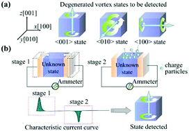
Here we propose a method to detect the degenerated tetragonal vortex states (i.e., the toroidal axis is along the x-, y- or z-axis) in ferroelectric nanodots by applying a controllable surface charge (CSC) condition. Electrodes are placed at two parallel surfaces of the nanodot to form a short circuit. Surface charges with a controllable density are then applied to another two parallel surfaces of the nanodot. Under this CSC condition, a characteristic short-circuit current vs. time (It) curve related with the evolution of domain structure in a nanodot can be detected. The evolution paths and the characteristic short-circuit It curves of the degenerated vortex states in ferroelectric nanodots have been systematically revealed by our phase field simulations by solving the time-dependent Ginzburg–Landau (TDGL) equations. It is found that the degenerated vortex states exhibit distinct evolution features under the CSC condition. In the stages of placing electrodes and increasing surface charges, one, two, and zero short-circuit It peak(s) are observed in the nanodots with 〈100〉, 〈010〉 and 〈001〉 vortex states, respectively. Therefore, the unknown vortex states of a nanodot can be distinguished. We further investigate the effects of temperature and nanodot size on the characteristic It curves of the vortex states. The results show that the vortex states can be nondestructively distinguished by applying the CSC condition if the nanodot size is within a moderate range (i.e., 8–12 nm). Our study provides an alternative way of detecting the degenerated tetragonal vortex states in ferroelectric nanodots without the use of a scanning probe microscope, and also sheds light on the application of ferroelectric vortex domain structures in novel devices such as memories, sensors and actuators.


Introduction

Because of their abundant functional properties, such as ferroelectricity, piezoelectricity and pyroelectricity, ferroelectric materials have attracted considerable attention from both academia and industry, and are prospective for developing electro-mechanical and electro-thermal sensors/actuators/transducers as well as high-density memories.1–6 For nanoscale ferroelectrics, the surface/interface effects further modify the material behaviors and lead to complex size effects. As a result, nanoscale ferroelectrics have been frequently found to exhibit novel or abnormal properties in comparison with the bulk counterparts.7–11 Particularly, an interesting kind of domain structure with the domains rotating in a closure, namely vortex domain structure (VDS), has been found in low-dimensional ferroelectric nanostructures under poor charge screening conditions.12,13 To exploit the potential applications of ferroelectric VDS, both theoretical and experimental works focused on the formation mechanisms, novel characteristics and controllability of VDS in various kinds of ferroelectric nanostructures.14–29

In the literature, using a first-principles-derived effective Hamiltonian approach, Naumov et al.13 predicted that low-dimensional ferroelectric systems under open-circuit condition form VDS to decrease the depolarization energy. The smallest vortex size was found about 3.2 nm, indicating that by using VDS to store information one can reach an ultimate storage density of 60 Tbit per inch2. A phase transition from a polar state to a vortex state by varying the screening condition of the depolarization field has also been further revealed.14 Based on molecular dynamics simulation, it has been found that ferroelectricity with a toroidal ordering can be sustained in nanoparticles with a few lattice constants.15 Meanwhile, quite a lot of researches have been taken on the controllability of VDS in ferroelectric nanostructures through electrical and mechanical means.17–23 Particularly, Prosandeev et al.18 showed that the single vortex state in asymmetric ferroelectric nanorings can be switched by a homogeneous electric field. Chen et al.19–22 studied the effects of mechanical loads on VDS, and found that mechanical loads can not only effectively control the vortex size and orientation but also lead to a novel vortex pining effect as well as the feasibility of vortex switching by a homogeneous electric field.

In contrast with the theoretical progresses, it remains a challenge to characterize and control the nanoscale ferroelectric VDS in experiments. Nevertheless, one can note that much experimental attempts have been made.25–29 For example, Hong et al.27 used focused ion beam technique to prepare well-shaped ferroelectric nanodots and observed VDS in the nanodots via scanning transmission electron microscope. Combining pulse laser deposition and piezoresponse force microscopy, Gao et al.28 prepared well-ordered ferroelectric nanodot arrays, and images of their measurements indicated the existence of bubble domain patterns in the nanodots. Balke et al.26 succeeded to control the formation of VDS in BiFeO3 film, and found an enhanced conductivity at the vortex core.29 With the further improvement of fabrication and characterization techniques in the near future, one can expect that more and more theoretically predicted features of the VDS could be revealed experimentally.

In another aspect, it is well known that a depolarization field would arise inside the ferroelectric if the surface polarization charges have not been completely screened. As a consequence, the domain structure of a ferroelectric can be controlled by varying the screening extent of surface polarization charges.14,30 For a typical capacitor structure, the surface polarization charges of the ferroelectric are compensated by the electron gas from the electrodes. The screening extent can be controlled by choosing proper electrodes. Screening of surface polarization charges can be also achieved by surface ionic charges, e.g., by those from atomic and molecular adsorbates.9,31,32 Interestingly, when placing a ferroelectric in a chemical environment, e.g., oxygen environment, surface redox reaction can occur, and then an electric field across the sample could be induced by the net charges generated during the reaction. In the literature, it was found that VDS of ferroelectric nanostructures are sensitive to the surface charge conditions.14 More recently, Wu et al.23 have predicted that fruitful domain patterns and evolution paths of VDS can be realized in the ferroelectric nanodots via applying a controllable surface charge (CSC) conditions to the nanodots. The sensitivity of VDS to the surface charge condition indicates potential applications of ferroelectrics on charge, gas or other nano-sensors.

For a regularly shaped nanostructure, its vortex states are not only degenerated in chirality but also degenerated in orientation. The typical examples include nanodots (e.g., PbTiO3) with degenerated tetragonal vortex states and nanodots (e.g., BaTiO3) with degenerated orthorhombic vortex states. It is natural to ask if we can distinguish these similar vortex states according to their signals during the same detection. While previous works on ferroelectric VDS focused on the formation and controllability of VDS,12–24,33 there were hardly any works on how to detect the vortex states except those using high resolution scanning probe microscopes to directly probe the local dipole states.27–29 In this paper, we propose a novel method to detect the degenerated tetragonal vortex states of cubic ferroelectric nanodots, and study the size and temperature effects on the domain evolution of the ferroelectric nanodots under a controllable surface charge (CSC) conditions. The distinct evolution behaviors of the degenerated vortex states and consequently the characteristic current vs. time (It) curves of the vortex states have been clearly revealed and completely summarized.

The physical model

In our work, a phase filed model of ferroelectric systems with a CSC condition is adopted to capture the evolution of domain structure. The spontaneous polarization is considered as the order P = (P1, P2, P3) parameter, which is associated with the spontaneous polar atomic displacements in a dielectric background material. The total polarization of a ferroelectric consists of the linear term PE and the nonlinear term P. The electric displacement field is expressed as D = ε0E + PE + P = ε0E + χbE + P = εbE + P, where ε0 is the dielectric constant of the vacuum. χb and εb are background susceptibility and background dielectric constant tensor,34–36 respectively.

The temporal evolution of the spontaneous polarization in ferroelectric nanodot can be simulated by solving the time-dependent Ginzburg–Landau (TDGL) equations, i.e., ∂Pi/∂t = −MδFPi (i = 1, 2, 3), where M is the kinetic coefficient related to the domain wall mobility, F is the total free energy, and t is time. In order to simulate the domain structure of ferroelectric materials in nanoscale, it is necessary to consider effects of inhomogeneous electromechanical fields as well as that of surface/interface on the total free energy of the system. In our simulations, the total free energy can be expressed as image file: c5ra25193a-t1.tif, where V and S are the volume and surface of the nanodot, respectively. fLand is the so-called Landau free energy density. fgrad stands for the density of gradient energy, which describes the free energy contributed by the spatial polarization variation. The mechanical stress field and its coupling with polarization contribute to the elastic energy density felas. felec is the density of electric energy, including the energy contributed by the depolarization field and external electric field. Due to the truncation of polarization near surfaces, an additional surface energy should be considered, and the surface energy density is fsurf.

A polynomial of Landau energy density fLand is written as37–39

image file: c5ra25193a-t2.tif
where α1 = (TT0)/(2ε0C0) is the dielectric stiffness, T is temperature, T0 and C0 are the Curie–Weiss temperature and Curie–Weiss constant, respectively. αij and αijk are the higher-order dielectric stiffness coefficients. The gradient energy density fgrad can be expressed by the gradients of the polarization field as fgrad = 1/2GijklPi,jPk,l, where Gijkl are gradient energy coefficients. The ferroelectric phase transition involves a structural change, which leads to the appearance of spontaneous strains ε0ij = QijklPkPl, with Qijkl being the electrostrictive coefficients. The elastic energy density felas can be expressed by felas = 1/2cijkleijekl = 1/2cijkl(εijε0ij)(εklε0kl), where cijkl are the elastic coefficients, eij = εijε0ij are the elastic strains, εij are the total strains. Since the background material is a cubic crystal structure, the background dielectric constants in three axial directions are the same. The electric energy density felec can be written as felec = −PiEi − 1/2εbEiEi.34,36,40 In our work, the upper and lower surfaces (along z direction) are exposed to a chemical environment and bonded with ionic surface charges (see Fig. 1b). A boundary condition with the surface charges is thus applied at these surfaces. The total electric field along z direction consists of the depolarization field Edep and the electric field induced by the ionic surface charges from the chemical environment Echem,41 i.e., E3 = Edep + Echem. The total electric field can be calculated by Ei = −ϕi, where ϕ is the electric potential. Supposing that no free charges exist inside the nanodot, the electric displacement Di satisfies the electrostatic equilibrium equation Di,i = 0. As shown in Fig. 1b, short-circuit and open-circuit boundary conditions are applied along x and y directions, respectively. For the short-circuit boundary condition, the electrostatic potential is zero at the surfaces of the ferroelectric nanodot.42 For the open-circuit boundary condition, we have Dini = 0 on the surfaces,23 where ni is the component of unit vector normal to the surfaces. According to the ref. 19, for the surfaces with ionic charges, the boundary condition can be written as Dini = σ, where σ is the surface charge density. Finally, the surface energy density fsurf can be written as fsurf = DiSPi2/2δeffi, where δeffi are the extrapolation lengths,43 DiS are the coefficients related to the gradient energy coefficients and surface orientation, DiS = G11ni + (G44 + G44)(nj + nk) (i, j, k = 1, 2, 3).21 One can deduce the boundary conditions as image file: c5ra25193a-t3.tif, with xj being the coordinate orientations and h being the length of simulated system.


image file: c5ra25193a-f1.tif
Fig. 1 Schematics of the method for detecting the degenerated vortex states in ferroelectric nanodots under a CSC condition. (a) Three degenerated vortex states (with the toroidal axis either along x-, y- or z-axis) to be detected, and (b) schematic of the detection. In stage 1, electrodes are placed at two parallel surfaces of the nanodot to form a close circuit. In stage 2, a CSC condition is applied to another two parallel surfaces. An unknown vortex state may be distinguished by its characteristic short-circuit It curve.

Simulation method

In the simulations, we employ cubic PbTiO3 nanodots with various sizes (i.e., the dimensions ranging from 6 nm to 14 nm) as models. Polarization distribution of the nanodot is obtained by solving discretized TDGL equations. Values of the expansion coefficients of the Landau potential, electrostrictive coefficients, elastic coefficients and extrapolation lengths7,38,44,45 are listed in Table 1 in the ESI. Domain patterns are characterized by the average polarization [P with combining macron] and the electric toroidal moment image file: c5ra25193a-t4.tif, r is the position vector.46 In addition, the nonzero toroidal moment (i.e., g ≠ 0) indicates that the toroidal order, which is a specific ordering of electric dipoles arranged in a loop, exists in the ferroelectric nanodots. To denote the paraelectric–ferroelectric transition, we also calculate the average magnitude of the polarization of all the sites, i.e., image file: c5ra25193a-t5.tif.

According to previous works,13,33 three degenerated tetragonal-like vortex domain patterns favor to form in the free-standing ferroelectric nanodot under the ideal open-circuit boundary condition as shown in Fig. 1a. Specifically, these three vortex states are defined as 〈100〉 (i.e., |gx| ≫ |gy| and |gz|), 〈010〉 (i.e., |gy| ≫ |gx| and |gz|) and 〈001〉 (i.e., |gz| ≫ |gx| and |gy|) vortex states, according to the direction of toroidal moment, which can be along 〈100〉, 〈010〉 and 〈001〉 axis direction, respectively. Generally, nanodots with different initial vortex orientations have different characteristics, e.g., different current–voltage signals under the same applied voltage. This is our starting point to propose a method to distinguish these three degenerated vortex states through detecting the It curves under a CSC condition.

The detection can be divided into two main stages, as shown in Fig. 1b. In stage 1, the short-circuit boundary condition is applied at the two parallel surfaces along 〈100〉 direction. This can be obtained by placing two parallel electrodes with ideal screening capability. Then, in stage 2, surface charges with a controllable density are applied to the upper and lower surfaces of the nanodot. The controllable negative or positive surface charges are produced by the adsorption reaction at the two surfaces. In general, the reaction and thus the amount of surface charges should be a strong function of the adsorption gas pressure. To simplify the calculation, we directly set the amount of the surface charge density to be σ to mimic the CSC condition, but ignore the detailed chemical equilibrium process.

As the short-circuit boundary condition is along 〈100〉 direction, a short-circuit current is generated related to the movement of screening charges in the electrodes. This charge movement is governed by the net polarization along 〈100〉 direction, i.e., 〈P1〉. The short-circuit current is given by I = dQe/dt = Sedqe/dt,47 where Qe is the total charge in the electrodes, Se is the area of the electrode, and dqe/dt is the current density. The above formula shows the positive correlation between the short-circuit current and the current density. dqe/dt is proportional to dP1/dt. For numerical stability of simulations, the following dimensionless variables are employed as image file: c5ra25193a-t6.tif, t* = |α0|Mt, P* = P/P0, ε*0 = |α0|ε0, α*1 = α1/|α0|, α*11 = α11P02/|α0|, α*12 = α12P02/|α0|, α*111 = α111P04/|α0|, α*112 = α112P04/|α0|, α*123 = α123P04/|α0|, Q*11 = Q11P02, Q*12 = Q12P02, Q*44 = Q44P02, s*11 = s11(|α0|P02), s*12 = s12(|α0|P02), s*44 = s44(|α0|P02), G*11 = G11/G110, G*12 = G12/G110, G*44 = G44/G110, G*44 = G44/G110, where α0 is the value of α1 at room temperature, P0 is the magnitude of the spontaneous polarization at room temperature, and G110 is a reference value of the gradient energy coefficients. To simplify the calculation, dP*1/dt* will be calculated instead of calculating the exact short-circuit current.

Results and discussions

Domain patterns with various sizes under ideal open-circuit condition

Domain patterns in cubic PbTiO3 nanodots with their sizes ranging from 6 nm to 14 nm are calculated under an ideal open-circuit condition. Note that, these domain patterns are all simulated by using a random perturbation as the initial input of TDGL equations. Fig. 2a shows the temperature dependence of the toroidal moment (gx, gy, gz) in the 8 × 8 × 8 nm3 nanodot with initial 〈001〉 vortex state. It can be seen that |gz| decreases as the temperature increases, and drops to zero when the temperature reaches ∼575 K, which is near the ferroelectric–paraelectric phase transition point. Similar results can be obtained in the 8 × 8 × 8 nm3 nanodots with initial 〈100〉 or 〈010〉 vortex state. The domain patterns of the three vortex states in the 8 × 8 × 8 nm3 nanodots at room temperature are shown in Fig. 2c. From the toroidal moment and domain patterns, one can clearly see that the three vortex states are tetragonal and degenerated. Because of the effect of depolarization field, the vortex domain patterns are energetically favorable to reduce the depolarization energy. To see the size effect, Fig. 2b shows |gz| with the nanodot size ranging from 6 nm to 14 nm. With the nanodot size increasing from 6 nm to 14 nm, the paraelectric–ferroelectric phase transition temperature increases from 475 K to 675 K because of the reduction of surface effect. As shown in Fig. 2d, one can also see that the tetragonal and degenerated vortex states can exist for all simulated sizes.
image file: c5ra25193a-f2.tif
Fig. 2 Simulated results of ferroelectric nanodot with various sizes under an ideal open-circuit boundary condition. (a) Toroidal moment components in 8 × 8 × 8 nm3 nanodot with 〈001〉 vortex state, (b) toroidal moment component |gz| in nanodots with 〈001〉 vortex states, (c) the equilibrium domain patterns of 8 × 8 × 8 nm3 nanodots with 〈100〉, 〈010〉, and 〈001〉 vortex states under T = 300 K, and (d) the equilibrium domain patterns of 〈001〉 vortex state in nanodots with different sizes under T = 300 K. All vortex domain patterns in the following figures are shown with the same color bar scale.

Domain evolution and characteristic short-circuit current under the CSC condition

In this section, we investigate the domain evolution and the characteristic It curves under the CSC condition. At room temperature, the toroidal moment and polarization in an 8 × 8 × 8 nm3 ferroelectric nanodot initially with the 〈100〉 vortex state are simulated and plotted in Fig. 3a and b, respectively. When placing the electrodes along 〈100〉 direction, |gx| keeps almost unchanged and |gy(z)| keeps near zero. Meanwhile, a net polarization image file: c5ra25193a-t7.tif along 〈100〉 direction of about 0.11 C m−2 is induced. As σ along the 〈001〉 direction increases, a net image file: c5ra25193a-t8.tif is induced and linearly increases with the increase of σ. Meanwhile, image file: c5ra25193a-t9.tif keeps a large value and |gx| decreases slowly when σ is lower than 0.2 C m−2, indicating that the toroidal order remains stable in the nanodot. When σ increases to ∼0.2 C m−2, |gx| drops to zero, and image file: c5ra25193a-t10.tif exhibits a sudden increase, indicating that the toroidal order disappears. Then, with a further increasing of σ, image file: c5ra25193a-t11.tif also decreases to zero, and image file: c5ra25193a-t12.tif increases linearly with σ.
image file: c5ra25193a-f3.tif
Fig. 3 Simulated results of a nanodot (8 × 8 × 8 nm3) with initial 〈100〉 vortex state at T = 300 K during the process of increasing σ. (a) Toroidal moment components, (b) polarization components, and (c) dependence of dP*1/dt* on σ. Corresponding domain patterns are also depicted at some selected points.

In Fig. 3c, dependence of dP*1/dt* on σ is plotted, and the corresponding domain patterns of selected points are also inset. During the detection, a current peak appears right after placing the electrodes. It could be explained by the simulated results shown in Fig. 3b. It is found that image file: c5ra25193a-t13.tif changes to a nonzero value when placing electrodes. Moreover, the vortex state also maintains in the nanodot. This coexistence of both net polarization and toroidal moment in the nanodot indicates that the domain state is actually a polar-vortex multi-order state. Then, comparing the corresponding domain patterns of labeled B and C points, we could find the vortex core shifts to the side surface of the nanodot with the increase of σ. This is because that an electric field along z-axis positive direction is formed by the surface charges to tilt the dipoles along the z-axis. When σ increases to ∼0.2 C m−2, the toroidal order disappears and a single c-domain state image file: c5ra25193a-t14.tif forms. Specially, image file: c5ra25193a-t15.tif changes from nonzero to null at this moment, but there is no obvious current change. That is because the change process is so long that the change of image file: c5ra25193a-t16.tif for each time step is very little. Then, the single c-domain is stable with the further increase of σ and there is no current peak.

As shown in Fig. 4a and b, for the nanodot initially with 〈010〉 vortex state, a sudden decrease of |gy| from ∼1.2 to 1.0 e Å−1 is observed after placing two parallel electrodes. As the surface charges is applied on the upper and lower surfaces, a net image file: c5ra25193a-t17.tif is induced and linearly increases with the increase of σ. Meanwhile, |gy| firstly increases a little bit and then gradually deceases to zero, indicating the vanishing of the toroidal ordering. When σ increases to 0.16 C m−2, image file: c5ra25193a-t18.tif drops from 0.38 to 0.11 C m−2. Then, with a further increase of σ, image file: c5ra25193a-t19.tif linearly increases with σ. As σ further increases to 0.36 C m−2, image file: c5ra25193a-t20.tif changes to zero and only image file: c5ra25193a-t21.tif keeps nonzero.


image file: c5ra25193a-f4.tif
Fig. 4 Simulated results of a nanodot (8 × 8 × 8 nm3) with initial 〈010〉 vortex state at T = 300 K during the process of increasing σ. (a) Toroidal moment components, (b) polarization components, and (c) dependence of dP*1/dt* on σ. Corresponding domain patterns are also depicted at some selected points.

From the corresponding domain patterns and dependence of dP*1/dt* on σ, a 180° domain pattern with a domain wall of ∼2 nm forms after placing the electrodes. As shown in Fig. 4c, this domain pattern is similar to that found in the BaTiO3 nanodot under the high charge screening condition.23 During the process of placing electrodes, image file: c5ra25193a-t22.tif keeps zero and no short-circuit current peak is observed. When σ increases to 0.16 C m−2, a current peak appears due to the change of domain structure from the 180° domain pattern to a single ac-domain pattern image file: c5ra25193a-t23.tif with the disappearance of domain wall. Then, with a further increase of σ, c-domain state forms, meanwhile, image file: c5ra25193a-t24.tif drops to ∼0 and another reverse current peak is observed.

Similar to the previous case, for the nanodot initially with 〈001〉 vortex state, |gz| suddenly decreases from ∼1.2 to 1.0 e Å−1 after placing two parallel electrodes (see Fig. 5a and b). With the increase of σ, |gz| decreases slowly and image file: c5ra25193a-t25.tif keeps increasing, while image file: c5ra25193a-t26.tif and image file: c5ra25193a-t27.tif keeps ∼0. When σ increases to ∼0.26 C m−2, |gz| drops to zero, and image file: c5ra25193a-t28.tif has a sudden increase from 0.1 C m−2 to 0.5 C m−2. Then, image file: c5ra25193a-t29.tif linearly increases with a further increase of σ. As shown in Fig. 5c, the short-circuit current peak has not been observed during the whole process of increasing σ. According to the domain patterns shown in Fig. 5c, a transformation from vortex state to 180° domain pattern with a domain wall of ∼2 nm is induced by placing electrodes. Then, domain wall tilts and gradually vanishes with the increase of σ. When σ increases to ∼0.26 C m−2, the 180° domain pattern disappears and a single c-domain pattern forms in the nanodot. For this nanodot initially with 〈001〉 vortex state, image file: c5ra25193a-t30.tif keeps ∼0 and no current peak can be detected during the detection.


image file: c5ra25193a-f5.tif
Fig. 5 Simulated results of a nanodot (8 × 8 × 8 nm3) with initial 〈001〉 vortex state at T = 300 K during the process of increasing σ. (a) Toroidal moment components, (b) polarization components, and (c) dependence of dP*1/dt* on σ. Corresponding domain patterns are also depicted at some selected points.

Summarizing the results in Fig. 3c, 4c and 5c, one can see that ferroelectric nanodots with degenerated tetragonal vortex states exhibit quite different behaviors during the detection. In order to clearly illustrate these behaviors, we plot the characteristic It curves of the 8 × 8 × 8 nm3 nanodots with degenerated vortex states under different temperatures as shown in Fig. 6. The domain patterns can be given as a function of temperature and σ, and represented by the phase diagrams in Fig. S1 in the ESI. In the detection, one, two and zero peak(s) in the It curves can be observed for the nanodots initially with 〈100〉, 〈010〉 and 〈001〉 vortex states, respectively. These interesting results indicate that an unknown vortex state in a ferroelectric nanodot could be distinguished by observing its characteristic short-circuit It curve, and the features of the It curves can't be affected by the temperature.


image file: c5ra25193a-f6.tif
Fig. 6 Dependence of dP*1/dt* on σ in nanodots (8 × 8 × 8 nm3) with 〈100〉, 〈010〉, and 〈100〉 vortex states under (a) T = 0 K, (b) T = 300 K, and (c) T = 400 K.

Domain pattern evolution with the decrease of surface charge density

According to the above results, the initial vortex orientation in a ferroelectric nanodot can be distinguished through the characteristic It curves during varying the CSC condition. Then, it is also important to ask whether the initial vortex state can reform after removing the surface charges and electrodes. If so, it is also an important finding for the behavior of the detection on the VDS being nondestructive. In this section, we thus simulate how the domain structure evolves in the process of decreasing σ and removing the electrodes. As shown in Fig. 7, a c-domain state forms at room temperature under the condition of σ = 0.6 C m−2 for all kinds of the nanodots. For the nanodot with initial 〈100〉 vortex state, image file: c5ra25193a-t31.tif decreases with the decrease of σ in the whole process of decreasing σ as shown in Fig. 7a. When σ decreases to 0.24 C m−2, image file: c5ra25193a-t32.tif becomes nonzero while |gx| keeps ∼0. Then, image file: c5ra25193a-t33.tif increases before σ decreases to 0.12 C m−2, and a polar-vortex state forms at σ = 0.12 C m−2. Meanwhile, image file: c5ra25193a-t34.tif drops from 0.18 to 0.11 C m−2, and image file: c5ra25193a-t35.tif drops from ∼0.35 to ∼0.1 C m−2 when σ decreases from 0.13 to 0.12 C m−2. With a further decrease of σ, image file: c5ra25193a-t36.tif keeps ∼0.11 C m−2 and image file: c5ra25193a-t37.tif lineally decreases. Finally, image file: c5ra25193a-t38.tif drops to zero at the moment of removing the electrodes, indicating vortex reconstructs. Comparing the initial and final values of polarizations and toroidal moment components in Fig. 7a and 3c, the domain pattern in the ferroelectric nanodot has not been destroyed in the whole detection.
image file: c5ra25193a-f7.tif
Fig. 7 Simulated results of toroidal moment components, polarization components (insets) of 8 × 8 × 8 nm3 nanodots at T = 300 K during the process of decreasing surface charge density. (a) Nanodot with 〈100〉 vortex state, (b) nanodot with 〈010〉 vortex state and (c) nanodot with 〈001〉 vortex state. Corresponding domain patterns of labeled points in the nanodots with (d) 〈100〉, (e) 〈010〉, and (f) 〈001〉 vortex states are shown.

As shown in Fig. 7b for the nanodot with initial 〈010〉 vortex state, image file: c5ra25193a-t39.tif lineally decreases until σ decreases to 0.25 C m−2. When σ decreases from 0.24 to 0.2 C m−2, image file: c5ra25193a-t40.tif increases from zero to 0.5 C m−2, and image file: c5ra25193a-t41.tif decreases from 0.44 to 0.13 C m−2. This indicates that an ac-domain state forms. Then, image file: c5ra25193a-t42.tif slowly increases with the decrease of σ, and image file: c5ra25193a-t43.tif lineally decreases. An a-domain state forms when the ionic surface charges are all removed. After the electrodes are removed, |gy| increases abruptly from zero to 1.2 e Å−1, indicating that the initial 〈010〉 vortex state re-forms. In the nanodot with 〈001〉 vortex state, the domain evolution is similar to the evolution of the nanodot with 〈010〉 vortex state as shown in Fig. 7c. The phase diagrams depicting the domain pattern are summarized in Fig. S2 in the ESI.

Note that c-domain state forms for all the three vortex states when the nanodot is under a high σ (Fig. 7). Generally, the single c-domain patterns evolved from the three vortex states have no obvious difference, and the re-formed vortex state could be along any one of the directions after the CSC condition is turned off. However, the nanodot could keep the initial vortex orientation after the processes of increasing and decreasing σ. Comparing the Fig. 7a–c, similar single domain patterns are obtained under the condition of σ = 0.6 C m−2, and small differences of polarization components can be observed. Here we consider that the single domain state under a high σ is related to the initial state, and these small differences can affect the domain evolution and determine the final domain structure. In a real measurement experiment consisting of several steps, it is not likely for a system to reach a totally stable state. Therefore, information related to the initial state will exist to affect the evolution of domain structure. Nevertheless, in practical application, we suggest using a lower upper limit of σ in the detection to avoid forming single domain.

Size effect on the characteristic current in ferroelectric nanodots

In following simulations, we would like to investigate the effect of nanodot size on the characteristic It curves, domain evolutions and final domain patterns. Fig. 8a–c show the evolution paths of polarization components and toroidal moment components (insets) in the 6 × 6 × 6 nm3 nanodots with initial 〈100〉, 〈010〉 and 〈001〉 vortex states, respectively. Under the short-circuit condition along x direction, the nonzero component of toroidal moment drops to zero and another two components of toroidal moment keep ∼0 in the nanodots. Meanwhile, image file: c5ra25193a-t44.tif jumps to a large nonzero value while another two components of polarization keep ∼0. Then, with the increase of σ, image file: c5ra25193a-t45.tif gradually decreases and drops to zero during the process of increasing σ. Meanwhile, image file: c5ra25193a-t46.tif keeps increasing with σ. Fig. 8d shows the dependence of dP*1/dt* on σ in the nanodots with initial 〈100〉, 〈010〉 and 〈001〉 vortex states. The characteristic It curves indicate that two opposite current peak can be observed for the nanodot with one of the initial degenerated vortex states. The first peak is induced by the placement of electrodes and the second peak appears during the process of increasing σ. From the corresponding domain patterns shown in Fig. 8e, the nanodots with three degenerated vortex states have similar domain evolution paths. During the process of increasing σ, the dipoles tilt to the positive z-axis direction and a single ac-domain state is stable. With a further increase of σ, the single ac-domain state transforms to a single c-domain state and the latter state keeps stable in the nanodot. Then, during the process of decreasing σ, the single c-domain state transforms to a single a-domain state in the nanodots with initial 〈100〉 and 〈001〉 vortex states after removing the ionic charges. Specially, the 〈010〉 vortex state re-forms in the nanodot when ionic charges are completely removed.
image file: c5ra25193a-f8.tif
Fig. 8 Simulated results of toroidal moment components, polarization components of 6 × 6 × 6 nm3 nanodots with initial (a) 〈100〉, (b) 〈010〉, and (c) 〈001〉 vortex states at T = 300 K. (d) Dependence of dP*1/dt* on σ of the three degenerated vortex states. Corresponding domain patterns in the nanodots with (e) 〈100〉, (f) 〈010〉, and (g) 〈001〉 vortex states during processes of increasing and decreasing σ.

Interestingly, the evolution behaviors of polarization and toroidal moment exhibit huge differences in the 14 × 14 × 14 nm3 nanodots with initial 〈100〉, 〈010〉 and 〈001〉 vortex states at room temperature. As shown in Fig. 9a, in the nanodot with initial 〈100〉 vortex state, |gx| drops from 2.06 e Å−1 to zero and image file: c5ra25193a-t47.tif increases from zero to 0.57 C m−2 when placing the electrodes on the 〈100〉 surfaces. Then, with the increase of σ, image file: c5ra25193a-t48.tif keeps decreasing and image file: c5ra25193a-t49.tif keeps increasing. After σ reaches 0.52 C m−2, image file: c5ra25193a-t50.tif drops to zero and image file: c5ra25193a-t51.tif has a large increase from 0.39 C m−2 to 0.62 C m−2. As shown in Fig. 9b, for the nanodot with initial 〈010〉 vortex state, |gy| decreases from 2.06 e Å−1 to 1.40 e Å−1 after placing the electrodes. Meanwhile, the components of polarization keep zero. With σ increasing, |gy| keeps unchanged and image file: c5ra25193a-t52.tif keeps increasing when σ is less than 0.1 C m−2. When σ increases to 0.12 C m−2, |gy| drops to zero and image file: c5ra25193a-t53.tif increases from 0.12 C m−2 to 0.41 C m−2. Then, image file: c5ra25193a-t54.tif linearly increases with the increase of σ. In the nanodot with initial 〈001〉 vortex state (see Fig. 9c), |gz| keeps a value of 2.06 e Å−1 when electrodes are placed on 〈100〉 surfaces. Meanwhile, another two components of toroidal moment and components of polarization always keep zero. |gz| gradually decreases and image file: c5ra25193a-t55.tif linearly increases with the increase of σ. When σ increases to 0.36 C m−2, |gz| drops to zero, image file: c5ra25193a-t56.tif has a sudden increase from zero to 0.53 C m−2, and image file: c5ra25193a-t57.tif has a small decrease. Then, with a further increase of σ, image file: c5ra25193a-t58.tif and image file: c5ra25193a-t59.tif linearly decreases and increases, respectively. image file: c5ra25193a-t60.tif suddenly decreases from 0.27 C m−2 to ∼0 and image file: c5ra25193a-t61.tif increases from 0.33 C m−2 to 0.57 C m−2 when σ increases to 0.54 C m−2.


image file: c5ra25193a-f9.tif
Fig. 9 Simulated results of toroidal moment components, polarization components of 14 × 14 × 14 nm3 nanodots with (a) 〈100〉, (b) 〈010〉, and (c) 〈001〉 vortex states at T = 300 K. (d) Dependence of dP*1/dt* on σ of the three degenerated vortex states. Corresponding domain structures in the nanodots with (e) 〈100〉, (f) 〈010〉, and (g) 〈001〉 vortex states during processes of increasing and decreasing σ.

The dependence of dP*1/dt* on σ in the 14 × 14 × 14 nm3 nanodots with initial 〈100〉, 〈010〉 and 〈001〉 vortex states is shown in Fig. 9d. A current peak appears with the placement of electrodes on the nanodot with initial 〈100〉 vortex state, while no current peaks are observed for the nanodot with initial 〈010〉 or 〈001〉 vortex state at this moment. With the increase of σ, a small current peak appears for the nanodot with initial 〈100〉 vortex state. Different with the results in 8 × 8 × 8 nm3 nanodot, there are no obvious current peaks for the nanodot with initial 〈010〉 vortex state throughout the whole process of increasing σ. For the nanodot with initial 〈001〉 vortex state, two weak opposite current peaks can be observed. The first peak appears with a sudden increase of image file: c5ra25193a-t62.tif and another peak appears because of the decrease of image file: c5ra25193a-t63.tif from a large value to zero. From the characteristic It curves, an unknown vortex state can be detected through this method. The corresponding domain patterns in the nanodots with initial 〈100〉, 〈010〉 and 〈001〉 vortex states are depicted in Fig. 9e–g, respectively. From the evolution of domain patterns during the process of decreasing σ, the evolution behaviors are similar for the nanodots with three degenerated vortex states. 90° domain forms when ionic surface charges are completely removed and a domain pattern with two 〈010〉 vortices forms in the nanodot after removing the electrodes. This indicates that the initial domain pattern has been destroyed after the detection. After the detection, the domain pattern transforms from a tetragonal-like vortex domain pattern to a vortex domain pattern with two 〈010〉 vortices.

To be more systematic, the dependence of dP*1/dt* on σ in the nanodots with their sizes ranging from 6 nm to 14 nm is summarized in Fig. 10. For the 6 × 6 × 6 nm3 nanodot with one of the degenerated vortex states, one current peak appears with the placement of electrodes. During the process of increasing σ, another reversed current peak can be observed. It is found that characteristic It curves for the nanodots with initial 〈100〉, 〈010〉 and 〈001〉 vortex states are similar. In addition, the similar results can be calculated in the nanodots with their sizes smaller than 6 nm, e.g., 4 nm (not given). For the nanodots with their sizes ranging from 8 nm to 12 nm, a current peak appears for the nanodots with initial 〈100〉 vortex state when placing two parallel electrodes on 〈100〉 direction, while no current peak is observed for nanodots with another two vortex states. With σ increasing, two opposite current peaks generate for the 8 × 8 × 8 nm3 and 10 × 10 × 10 nm3 nanodots with initial 〈010〉 vortex state, and one current peak is observed for the 12 × 12 × 12 nm3 nanodot with initial 〈010〉 vortex state. Thus, the degenerated vortex states in the nanodot could be distinguished by their characteristic It curves. And the final domain patterns are the same with the initial domain patterns, indicating that the detection is nondestructive. In the 14 × 14 × 14 nm3 nanodot, two opposite current peaks generate for the nanodots with initial 〈100〉 and 〈001〉 vortex states while current peaks cannot be detected in the nanodot with initial 〈010〉 vortex state. Differently, in the nanodot with initial 〈100〉 vortex state, one strong current peak is induced by the placement of electrodes and another weak current peak appears during the process of increasing σ. While both of the opposite current peaks for the nanodot with initial 〈001〉 vortex state are detected in the process of increasing σ. Three degenerated vortex states exhibit distinct evolution behaviors. But the final domain patterns shown in Fig. 9e and f indicate that the initial vortex domain states transform from a tetragonal-like vortex domain state to a vortex domain state with two 〈010〉 vortices. The initial domain pattern is thus destroyed during the detection. Moreover, the initial domain pattern in a larger nanodot, i.e., 16 nm, also is destroyed according to the simulated results.


image file: c5ra25193a-f10.tif
Fig. 10 A summary of the dependence of dP*1/dt* on σ in the nanodots with their dimensions ranging from 6 nm to 14 nm.

Conclusions

In summary, to find a method to detect the vortex states which are degenerated in orientation, we investigate the vortex domain evolution of the ferroelectric nanodots under a CSC condition. The evolution characteristics of the degenerated vortex states and the effects of the nanodot size as well as temperature have been comprehensively revealed. Our results show distinct evolution characteristics of the degenerated vortex states in the nanodots with their sizes ranging from 6 nm to 14 nm, and indicate that the size effects on the domain structure evolution under the CSC condition are significant. Importantly, we calculate the characteristic short-circuit It curves related with the evolution of domain structure in the nanodots. In the processes of placing electrodes and increasing surface charges, we observe one, two or zero peak(s) of the It curve for the nanodots with initial 〈100〉, 〈010〉, or 〈001〉 vortex states, respectively. Then, the characteristic It curves for all of the nanodots with their sizes ranging from 6 nm to 14 nm are systematically simulated and discussed. It is thus possible to distinguish the vortex states by their characteristic It curves. One can nondestructively distinguish the vortex states of a nanodot by applying the CSC condition if its size is in-between a moderate range. Moreover, the vortex state should be distinguished in the nanodot with defect under this CSC condition. Interestingly, according to previous work,48 the vortex core can be pinned by the defect. Thus, the kind of defect may be understood by analyzing the It curve, which is related to the vortex orientation. We also note that degenerated rhombohedral vortex states in BaTiO3 exhibit distinct It curves under the CSC condition and we would like to take a systematic investigation in the future works.

Acknowledgements

The authors acknowledge the financial support of the National Key Basic Research Program of China (No. 2015CB351905), the National Natural Science Foundation of China (NSFC) (No. 11474363, 11232015, 11472313). Yue Zheng also thanks support from the Fundamental Research Funds for the Central Universities, NSFC-Guangdong Government Joint Fund for Super Computational Research and Application, Fok Ying Tung Foundation and Guangdong Natural Science Funds for Distinguished Young Scholar.

References

  1. T. Chen and J. F. Scott, Integr. Ferroelectr., 1993, 3, 69–80 CrossRef CAS.
  2. S.-E. Park and T. R. Shrout, J. Appl. Phys., 1997, 82, 1804 CrossRef CAS.
  3. O. Auciello and J. F. Scott, Phys. Today, 1998, 51, 22 CrossRef CAS.
  4. Y. Zheng and C. H. Woo, Nanotechnology, 2009, 20, 075401 CrossRef PubMed.
  5. A. N. Morozovska, E. A. Eliseev, M. D. Glinchuk and R. Blinc, Phys. Rev. B: Condens. Matter Mater. Phys., 2010, 81, 092101 CrossRef.
  6. T. H. E. Lahtinen, K. J. A. Franke and S. van Dijken, Sci. Rep., 2012, 2, 258 Search PubMed.
  7. W. L. Zhong, Y. G. Wang, P. L. Zhang and B. D. Qu, Phys. Rev. B: Condens. Matter Mater. Phys., 1994, 50, 698 CrossRef CAS.
  8. C. H. Ahn, K. M. Rabe and J.-M. Triscone, Science, 2004, 303, 488 CrossRef CAS PubMed.
  9. J. E. Spanier, A. M. Kolpak, J. J. Urban, I. Grinberg, L. Ouyang, W. S. Yun, A. M. Rappa and H. Park, Nano Lett., 2006, 6, 735–739 CrossRef CAS PubMed.
  10. A. Schilling, R. M. Bowman, J. M. Gregg, G. Catalan and J. F. Scott, Appl. Phys. Lett., 2006, 89, 212902 CrossRef.
  11. Y. Zheng, W. J. Chen, X. Luo, B. Wang and C. H. Woo, Acta Mater., 2012, 60, 1857 CrossRef CAS.
  12. H. Fu and L. Bellaiche, Phys. Rev. Lett., 2003, 91, 257601 CrossRef PubMed.
  13. I. I. Naumov, L. Bellaiche and H. Fu, Nature, 2004, 432, 737 CrossRef CAS PubMed.
  14. I. Ponomareva, I. I. Naumov and L. Bellaiche, Phys. Rev. B: Condens. Matter Mater. Phys., 2005, 72, 214118 CrossRef.
  15. M. G. Stachiotti and M. Sepliarsky, Phys. Rev. Lett., 2011, 106, 137601 CrossRef CAS PubMed.
  16. I. Münch and J. E. Huber, Appl. Phys. Lett., 2009, 95, 022913 CrossRef.
  17. B.-K. Lai, I. Ponomareva, I. I. Naumov, I. Kornev, H. Fu, L. Bellaiche and G. J. Salamo, Phys. Rev. Lett., 2006, 96, 137602 CrossRef PubMed.
  18. S. Prosandeev, I. Ponomareva, I. Kornev and L. Bellaiche, Phys. Rev. Lett., 2008, 100, 047201 CrossRef CAS PubMed.
  19. W. J. Chen, Y. Zheng and B. Wang, Appl. Phys. Lett., 2012, 100, 062901 CrossRef.
  20. W. J. Chen, Y. Zheng and B. Wang, Sci. Rep., 2012, 2, 796 CAS.
  21. W. J. Chen, Y. Zheng, B. Wang, D. C. Ma and F. R. Ling, Phys. Chem. Chem. Phys., 2013, 15, 7277 RSC.
  22. W. J. Chen and Y. Zheng, Acta Mater., 2015, 88, 41 CrossRef CAS.
  23. C. M. Wu, W. J. Chen, Y. Zheng, D. C. Ma, B. Wang, J. Y. Liu and C. H. Woo, Sci. Rep., 2014, 4, 3946 CAS.
  24. J. Y. Liu, W. J. Chen, B. Wang and Y. Zheng, J. Appl. Phys., 2013, 114, 044101 CrossRef.
  25. B. J. Rodriguez, X. S. Gao, L. F. Liu, W. Lee, I. I. Naumov, A. M. Bratkovsky, D. Hesse and M. Alexe, Nano Lett., 2009, 9, 1127 CrossRef CAS PubMed.
  26. N. Balke, S. Choudhury, S. Jesse, M. Huijben, Y. H. Chu, A. P. Baddorf, L. Q. Chen, R. Ramesh and S. V. Kalinin, Nat. Nanotechnol., 2009, 4, 868 CrossRef CAS PubMed.
  27. J. Kim, J. Hong, M. Park, W. Zhe, D. Kim, Y. J. Jang, D. H. Kim and K. No, Adv. Funct. Mater., 2011, 21, 4277 CrossRef CAS.
  28. X. S. Gao, F. Xue, M. H. Qin, J. M. Liu, B. J. Rodriguez, L. F. Liu, M. Alexe and D. Hesse, J. Appl. Phys., 2011, 110, 052006 CrossRef.
  29. N. Balke, B. Winchester, W. Ren, Y. H. Chu, A. N. Morozovska, E. A. Eliseev, M. Huijben, R. K. Vasudevan, P. maksymovych, J. Britson, S. Jesse, I. Kornev, R. Ramesh, L. Bellaiche, L. Q. Chen and S. V. Kalinin, Nat. Phys., 2012, 8, 81 CrossRef CAS.
  30. Y. L. Li, S. Y. Hu, Z. K. Liu and L. Q. Chen, Appl. Phys. Lett., 2002, 81, 427 CrossRef CAS.
  31. G. B. Stephenson and M. J. Highland, Phys. Rev. B: Condens. Matter Mater. Phys., 2011, 84, 064107 CrossRef.
  32. Y. Kim, I. Vrejoiu, D. Hesse and M. Alexe, Appl. Phys. Lett., 2010, 96, 202902 CrossRef.
  33. S. Prosandeev and L. Bellaiche, Phys. Rev. B: Condens. Matter Mater. Phys., 2007, 75, 094102 CrossRef.
  34. C. H. Woo and Y. Zheng, Appl. Phys. A, 2008, 91, 59 CrossRef CAS.
  35. A. K. Tagantsev, Ferroelectrics, 2008, 375, 19 CrossRef CAS.
  36. Y. Zheng and C. H. Woo, Appl. Phys. A, 2009, 97, 617 CrossRef CAS.
  37. M. J. Haun, E. Furman, S. J. Jang, H. A. McKinstry and L. E. Cross, J. Appl. Phys., 1987, 62, 3331 CrossRef CAS.
  38. Y. L. Li, L. E. Cross and L. Q. Chen, J. Appl. Phys., 2005, 98, 064101 CrossRef.
  39. Y. L. Wang, A. K. Tagantsev, D. Damjanovic, N. Setter, V. K. Yarmarkin and A. I. Sokolov, Phys. Rev. B: Condens. Matter Mater. Phys., 2006, 73, 132103 CrossRef.
  40. L. D. Landau, E. M. Lifshitz and L. P. Pitaevskii, Electrodynamics of Continuous Media, Oxford University Press, Oxford, 1984 Search PubMed.
  41. D. C. Ma, Y. Zheng, B. Wang and C. H. Woo, Appl. Phys. Lett., 2011, 99, 142908 CrossRef.
  42. J. Wang and T. Y. Zhang, Phys. Rev. B: Condens. Matter Mater. Phys., 2006, 73, 144107 CrossRef.
  43. R. Kretschmer and K. Binder, Phys. Rev. B: Condens. Matter Mater. Phys., 1979, 20, 1065 CrossRef CAS.
  44. T. Sluka, A. K. Tagantsev, D. Damjanovic, M. Gureev and N. Setter, Nat. Commun., 2012, 3, 748 CrossRef PubMed.
  45. J. Hlinka and P. Márton, Phys. Rev. B: Condens. Matter Mater. Phys., 2006, 74, 104104 CrossRef.
  46. S. Prosandeev, I. Ponomareva, I. Naumov, I. Kornev and L. Bellaiche, J. Phys.: Condens. Matter, 2008, 20, 193201 CrossRef.
  47. Y. Zheng, C. H. Woo and B. Wang, Nano Lett., 2008, 8, 3131 CrossRef CAS PubMed.
  48. W. J. Chen, Y. Zheng and B. Wang, Appl. Phys. Lett., 2014, 104, 222912 CrossRef.

Footnote

Electronic supplementary information (ESI) available. See DOI: 10.1039/c5ra25193a

This journal is © The Royal Society of Chemistry 2016