DOI:
10.1039/C5QI00242G
(Review Article)
Inorg. Chem. Front., 2016,
3, 452-463
Intercalation in two-dimensional transition metal chalcogenides
Received
6th November 2015
, Accepted 8th January 2016
First published on 12th January 2016
Abstract
Intercalation is a reversible insertion process of foreign species into crystal gaps. Layered materials are good host materials for various intercalant species ranging from small ions to atoms to molecules. Given the recent intense interest in two-dimensional (2D) layered materials in thin limits, this review highlights the opportunities that intercalation chemistry can provide for nanoscale layered materials. Novel heterostructures or emergent electrical properties not found in the intrinsic host materials are possible with intercalation. In particular, we review various exfoliation methods developed for 2D layered nanomaterials based on intercalation chemistry and extensive tuning of the electrical, optical, and magnetic properties of 2D layered materials due to intercalation.
 Judy J. Cha | Judy J. Cha is the Carol and Douglas Melamed Assistant Professor in the Department of Mechanical Engineering and Materials Science at Yale University, CT, USA. She is a member of Energy Sciences Institute at Yale West Campus. Her current research includes two-dimensional chalcogenide thin films and nanostructures for energy and novel electronic applications, and topological insulator and topological crystalline insulator nanostructures for fundamental condensed matter studies. |
1. Brief history of intercalation into bulk transition metal chalcogenides
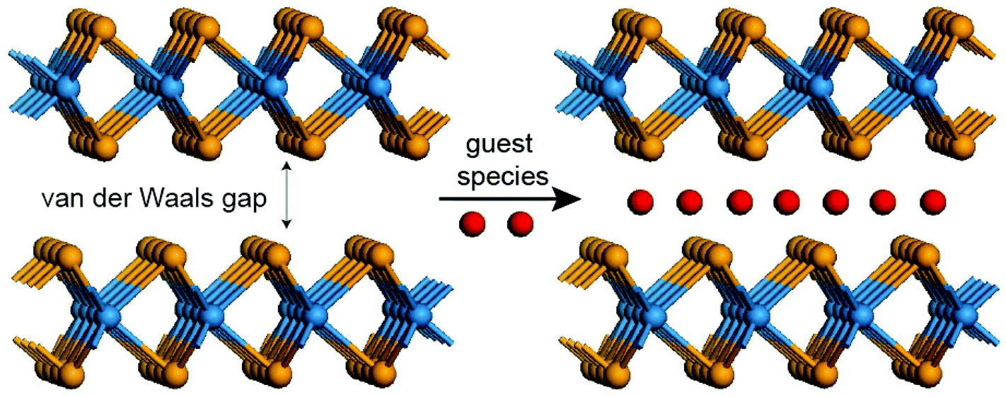
Bulk layered materials have been studied extensively in the past several decades because of their unique structural features, and physical and chemical properties.1 The rich family of layered materials consists of single-element crystals, such as graphite, phosphorus, arsenic, antimony and bismuth, silicates, hydroxides, organic compounds such as rubrene (C42H28) and dioctylbenzothienobenzothiophene (C8-BTBT), and inorganic compounds such as transition metal chalcogenides and many oxides.2–7 Layered materials typically exhibit strong in-plane covalent bonding and weak out-of-plane van der Waals interactions through the interlayer gap.8 They exhibit a wide range of electronic band structures from insulators, semiconductors, metals, superconductors to topological insulators.8–11 Here we limit ourselves specifically to transition metal chalcogenides, which are usually referred to as MX2 and MX, where M represents a transition metal from group 4 to group 10 (such as Nb, Mo, Ti, V, Hf, Ta, W, Fe), and X represents a chalcogen (S, Se, and Te). Owing to the layered structure with a rather large interlayer gap, intercalation into transition metal chalcogenides is easily achieved for fundamental studies as well as for technological applications (Fig. 1).12,13
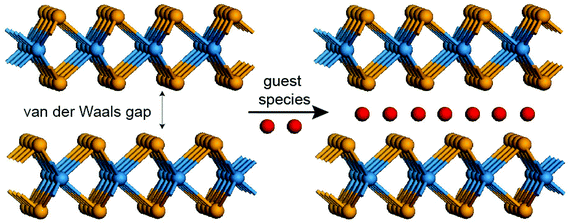 |
| | Fig. 1 Schematic for intercalation in the TMD-type layered materials, where guest species can be inserted into the van der Waals gap by diverse methods. | |
Intercalation is a chemical process to reversibly insert foreign species at the crystal gap. Intercalation layered materials have been paid much attention in condensed matter physics and electrochemical energy devices. In condensed matter physics, intercalating transition metal dichalcogenides (TMDs) with ions leads to charge density waves, two-dimensional superconductivity, and interesting phase transitions.14,15 The most well-known electrochemical energy device using intercalation is a Li-ion battery in which Li-ions are intercalated at the van der Waals gaps reversibly for charging and discharging. The field of intercalation in layered materials has grown dramatically since the appearance of a large class of graphite intercalation compounds.14 Intercalation into TMDs has been successfully achieved by chemical vapor transport, electrochemical methods, ion exchange, and oxide-reduction methods, in which the guest species introduced into the van der Waals gaps can be atoms, ions and molecules.8,16 Intercalation can change the band filling state and the Fermi level, resulting in superconductivity, charge density waves and the Peierls instability. For example, Geballe et al. reported a large class of organic molecule-intercalated TMDs as new superconductors.17 In addition, Prober et al. showed that the dimensionality of the superconductivity in (Pyridine)1/2TaS2 intercalation compounds is in accord with the qualitative predictions of the Lawrence–Doniach theory for weakly-coupled superconducting layers.18
2. Brief introduction of two-dimensional transition metal chalcogenides
As the first atomically thin two-dimensional (2D) crystal composed of a sp2-bonded carbon framework, graphene has been extensively studied and used as device platforms in condense matter physics, chemistry and materials science due to its fascinating properties such as ultrahigh mobility (∼200![[thin space (1/6-em)]](https://www.rsc.org/images/entities/char_2009.gif) 000 cm2 V−1 s−1), amazing optical transparency (∼97.7%), and high thermal conductivity (∼5300 W m−1 K−1).19 Following graphene, interest in 2D layered materials has rapidly grown, particularly for TMDs.20 Several applications have been demonstrated using 2D TMDs such as field effect transistors based on monolayer MoS2,21 optoelectronic devices based on monolayer and few-layered MoS2 and WSe2,22 piezoelectric devices based on odd-layered TMDs (MoS2, WS2, MoSe2 and WSe2)23,24 and electrochemical electrodes based on few-layered MoS2 and WS2.25 In the case of 2D TMDs (for example, MoS2), indirect-to-direct bandgap transition properties and valley physics emerge when the thickness decreases to a monolayer regime.26 In addition, inversion symmetry can be broken when thinned down to a single atomic layer, exhibiting novel properties such as large second-order nonlinear susceptibility, valley-selective circular dichroism and piezoelectricity.23,27,28 Polymorphism has also been observed in 2D TMDs. Generally several crystal structures are possible for TMDs such as 1T, 1T′, and 2H. 1T phase TMDs are an excellent candidate for electrochemical catalysts because of their enhanced conductivity and reduced reaction free energy.29 For example, vertically aligned TMD layers and graphene–TMD composites create a large number of catalytically active edge sites, significantly enhancing the hydrogen evolution reaction performance.29–32 By vertically stacking 2D materials with different bandgaps and work functions, van der Waals heterostructures can be achieved to tune their electrical properties. Field effect tunneling transistors are reported as the first application of such tunability, in which MoS2 or WS2 serves as a vertical transport barrier.33 Graphene–WS2–graphene vertical devices have been successfully demonstrated as a gate tunable photovoltaic device with high external quantum efficiency.34 An atomically sharp heterostructure formed by stacking two different TMDs, atomically thin layers of WSe2 (p-type semiconductor) and MoS2 (n-type semiconductor), has shown diode behavior in the dark state and the photovoltaic effect upon illumination.35 Forming p–n heterostructures using monolayer TMDs in the lateral direction is important for atomically thin field effect transistors, inverters, operational unit and digital circuits. Using the electrostatic gate doping and chemical vapor deposition doping growth method, a WSe2 based lateral p–n junction showed impressive electronic and optoelectronic properties.36,37 Intercalation reaction offers another degree of freedom to achieve novel 2D layered materials and redesign and improve materials properties. Intercalation chemistry is critical for the exfoliation of 2D TMDs, tuning the physical properties such as electricity, thermoelectricity and superconductivity, and phase change for catalyst applications.
000 cm2 V−1 s−1), amazing optical transparency (∼97.7%), and high thermal conductivity (∼5300 W m−1 K−1).19 Following graphene, interest in 2D layered materials has rapidly grown, particularly for TMDs.20 Several applications have been demonstrated using 2D TMDs such as field effect transistors based on monolayer MoS2,21 optoelectronic devices based on monolayer and few-layered MoS2 and WSe2,22 piezoelectric devices based on odd-layered TMDs (MoS2, WS2, MoSe2 and WSe2)23,24 and electrochemical electrodes based on few-layered MoS2 and WS2.25 In the case of 2D TMDs (for example, MoS2), indirect-to-direct bandgap transition properties and valley physics emerge when the thickness decreases to a monolayer regime.26 In addition, inversion symmetry can be broken when thinned down to a single atomic layer, exhibiting novel properties such as large second-order nonlinear susceptibility, valley-selective circular dichroism and piezoelectricity.23,27,28 Polymorphism has also been observed in 2D TMDs. Generally several crystal structures are possible for TMDs such as 1T, 1T′, and 2H. 1T phase TMDs are an excellent candidate for electrochemical catalysts because of their enhanced conductivity and reduced reaction free energy.29 For example, vertically aligned TMD layers and graphene–TMD composites create a large number of catalytically active edge sites, significantly enhancing the hydrogen evolution reaction performance.29–32 By vertically stacking 2D materials with different bandgaps and work functions, van der Waals heterostructures can be achieved to tune their electrical properties. Field effect tunneling transistors are reported as the first application of such tunability, in which MoS2 or WS2 serves as a vertical transport barrier.33 Graphene–WS2–graphene vertical devices have been successfully demonstrated as a gate tunable photovoltaic device with high external quantum efficiency.34 An atomically sharp heterostructure formed by stacking two different TMDs, atomically thin layers of WSe2 (p-type semiconductor) and MoS2 (n-type semiconductor), has shown diode behavior in the dark state and the photovoltaic effect upon illumination.35 Forming p–n heterostructures using monolayer TMDs in the lateral direction is important for atomically thin field effect transistors, inverters, operational unit and digital circuits. Using the electrostatic gate doping and chemical vapor deposition doping growth method, a WSe2 based lateral p–n junction showed impressive electronic and optoelectronic properties.36,37 Intercalation reaction offers another degree of freedom to achieve novel 2D layered materials and redesign and improve materials properties. Intercalation chemistry is critical for the exfoliation of 2D TMDs, tuning the physical properties such as electricity, thermoelectricity and superconductivity, and phase change for catalyst applications.
3. Intercalation in 2D TMDs
3.1 Intercalation methods for exfoliation of 2D TMDs
This section reviews intercalation methodologies for various 2D layered materials, while mainly focusing on intercalation-assisted exfoliations of 2D TMDs.
3.1.1 Earlier approaches: oxidation–reduction chemistry.
Historically, intercalation has been applied to 2D materials as a means of exfoliating individual 2D layers from their bulk counterparts in large quantities. Exfoliation of 2D materials was initially developed for graphite, which involves the manual rubbing and peeling of bulk graphite.38 However, such mechanical exfoliation suffers from low-yield production of the desired materials, and thus is technologically non-scalable. Following the successful demonstration of the mechanical exfoliation, liquid-based exfoliation of layered materials was developed.39–41 In contrast to the mechanical exfoliation, liquid-based exfoliation presents great advantages of versatility, scalability, and reliability for the mass production of 2D materials, and thus is compatible with industrial scale techniques. Intercalation chemistry plays a key role in a majority of the liquid-based exfoliation methods. The underlying principle for the intercalation-based exfoliation is in increasing the interlayer spacing between individual 2D layers by inserting foreign species. This will weaken the interlayer adhesion and reduce the energy barrier to exfoliation, thus eventually increase the accessible surface areas in 2D materials.40 One of the earliest exfoliation methods based on intercalation was developed for graphite, which involves oxidation–reduction chemistry. In this approach pioneered by Ruoff et al.42 graphite is oxidized by oxidizers such as sulfuric acid, which results in the attachment of hydroxyl groups to the graphene basal plane, causing hydrophilic surfaces. Then the oxidized graphite is dispersed in solvents, which allows for the intercalation of water molecules and the subsequent separation of 2D layers – graphene oxide – due to the enhanced hydrophilicity. The dispersed graphene oxides are subsequently stabilized against re-aggregation by chemical reduction, which removes most of the oxide residues. Layered crystals are particularly suitable for intercalation processes as they can strongly adsorb guest species into their van der Waals gaps between each layer, forming the basis of intercalation-based exfoliations of a variety of 2D materials, including 2D TMDs.8 A major drawback of this method is that it introduces a significant amount of chemical groups and structural defects on the exfoliated materials. Thus, the physical properties of graphene exfoliated via the oxidation–reduction intercalations are quite different from those of its pristine form.42,43 For example, the electrical conductivity of the graphene obtained via intercalation is generally lower than that of the mechanically exfoliated intercalation due to the enhanced electron scattering from the structural defects.
3.1.2 Organic material-based ion exchange intercalation.
Some intercalants can transfer charges to targeted layers, lowering the interlayer binding strength of 2D layers. In general, ion exchange intercalations are based on the fact that some layered materials contain cationic counterions in 2D layers which can be exchanged for protons for charge neutrality by being dissolved in solvents.40 The intercalated 2D layers are then easily exfoliated by various physical means such as shear mixing or ultrasonic waves.8,40 Earlier work can be found with the exfoliation of layered metal oxides developed over decades ago.44,45 Recently, ion-exchange intercalations have been widely employed to exfoliate a variety of 2D materials including graphene and 2D TMDs. A few-layered graphene has been exfoliated from graphite via the intercalation of ionic compounds such as iodine chloride (ICl) or iodine bromide (IBr).46 For the exfoliation of 2D TMDs, organic-based intercalants such as n-butyllithium have been initially developed and applied to exfoliate single-layer 2D MoS2.8,47 In these approaches, organic ions can be intercalated into neutralized 2D interlayers by proton exchange, which leads to substantial swelling in between the 2D layers as in the case of water-intercalations for graphite.41Fig. 2(a) illustrates a schematic for the ion-exchange intercalation. Efforts to increase the scalability of intercalated 2D TMDs have been continuously pursued and various alkyl amines are used as intercalants; these include n-butylamine (BA), n-octylamine (OA), n-dodecylamine (DDA), and n-octadecylamine (ODA).48,49 Ammonia ion-based intercalations have also been developed for the exfoliation of 2D WS2.50 Recently, high-yield exfoliation of 2D TMDs has been achieved by using hydrazine (N2H4) as an intercalant.51 Bulk TMD crystals are expanded by reacting them with N2H4 under hydrothermal conditions, which is enabled by a redox rearrangement model in which part of the N2H4 is oxidized to N2H5 upon intercalation.51 Expanded TMDs react with alkali naphthalenide solution, and then exfoliate to single layers in water. Fig. 2(b)–(d) illustrates a schematic for the N2H4 based intercalations of various TMDs. Despite their versatility, one major drawback of the ion exchange-based intercalation approaches is their high sensitivity to ambient conditions, which limits the number of species to be intercalated into 2D materials.
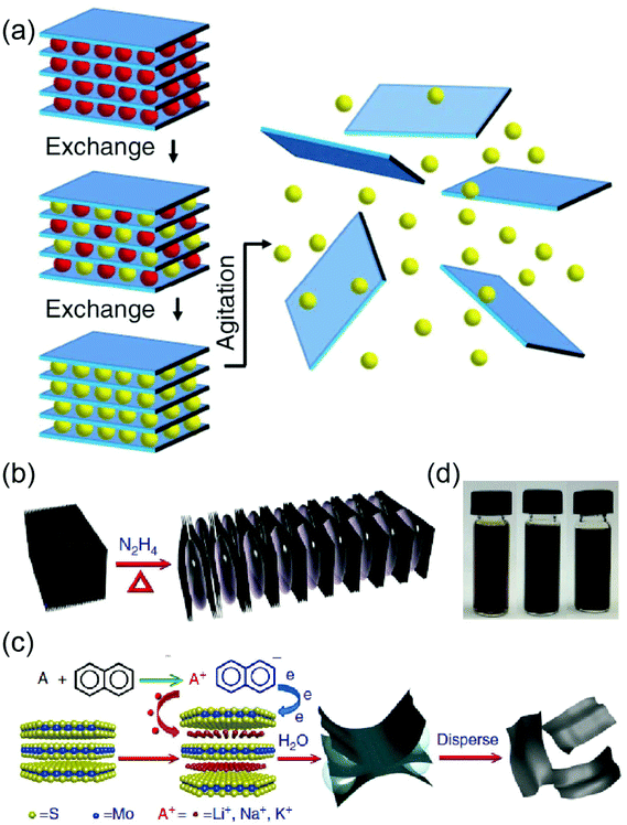 |
| | Fig. 2 (a) Schematic for ion exchange intercalation of 2D TMDs. Some layered materials contain ions between 2D layers so as to balance surface charge on the layers. These ions (red spheres) can be exchanged for other ions (yellow spheres) in a liquid environment (from ref. 40). (b–d) Large-yield exfoliation of 2D MoS2 and other TMDs via N2H4 intercalations. (b) Bulk MoS2 reacts with N2H4, resulting in swollen 2D layers. (c) The reacted MoS2 subsequently intercalates with alkali naphthalenide solution (A+ C10H8−) and then exfoliates to single MoS2 layers. (d) Large-scale exfoliation of other TMDs; TiS2 (left) TaS2 (mid) NbS2 (right) (from ref. 51). | |
3.1.3 Zerovalent chemistry intercalation.
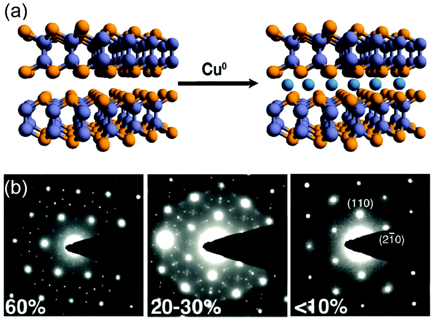
The degree of intercalation in 2D materials is determined by many factors such as (1) physical size of intercalating species, (2) charge stage of intercalating species, and (3) structural stability of hosting materials after intercalation. In many cases, the intercalation of 2D materials is driven by the tendency for retaining the charge neutrality.13 This is enabled by either a change of the oxidation states or by the presence of atomic vacancies to accommodate the charge neutrality. Intercalation of alkali metals such as lithium is relatively facile due to their small sizes irrespective of their charge states while the ionic nature of the intercalant critically determines the extent of intercalation in many cases. In this respect, zerovalent intercalation methods recently developed by Cui and Koski offer following advantages uniquely suitable for the intercalation of 2D materials;13 (1) It does not require a change in the oxidation state of hosting materials. This advantage allows the intercalation of various zerovalent metals (e.g., Ag, Au, Co, Cu, Fe, In, Ni and Sn) into 2D TMDs and realization of their superstoichiometric compositions.52 (2) It does not disrupt the hosting 2D layered structures, thus allowing a high degree of intercalation. For example, nearly 60 atomic percent of zerovalant Cu has been intercalated into Bi2Se3 layered crystals.53,54Fig. 3(a) illustrates a schematic for the zerovalent intercalation and Fig. 3(b) shows a variety of superlattice patterns observed upon the intercalation of Cu into Bi2Se3. The intercalation reaction is typically carried out by incorporating metal element containing precursors (e.g., tetrakis(acetonitrile)copper(I)hexafluorophosphate for Cu intercalation) into source materials under reflux at elevated temperatures.53 These methods have been further extended to intercalate various TMDs (e.g., Sb2Te3, In2Se3, GaSe)53 and non-TMDs such as MoO355 as well as, incorporating dual metal elements into them.56 They have been employed not only for exfoliating 2D materials, but also for focusing more on tuning their various physical properties which will be discussed in detail later in this Review.
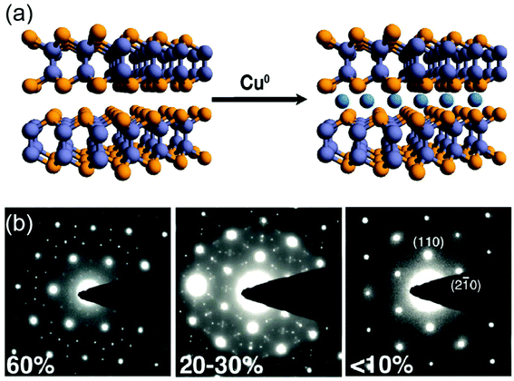 |
| | Fig. 3 (a) Schematic for zerovalent metal intercalation into 2D TMDs. (from ref. 53). (b) Electron diffraction patterns of Bi2Se3 upon Cu intercalation, showing a variety of superlattice structures accommodating nearly 60% of Cu (from ref. 54). | |
3.1.4 Electrochemical intercalation.
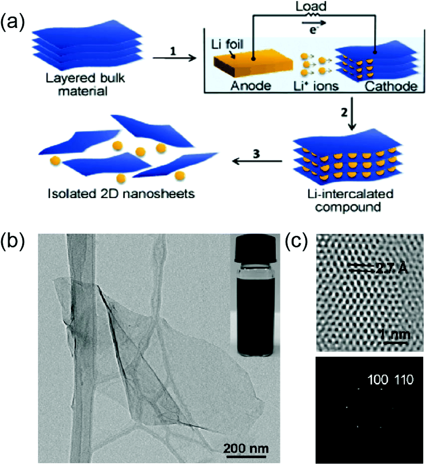
Electrochemical reactions mainly developed for lithium (Li) ion batteries or supercapacitors can be used to tune the electronic structure and chemical potential of 2D materials by intercalating ions. In these approaches, either cations or anions can be electrochemically intercalated into the van der Waals gap of 2D materials or reacted with 2D crystalline lattices themselves via a simple electrochemical reaction.13 One of the most extensively employed electrochemical approaches is the intercalation of a Li ion based on the following; for the case of MoS2 intercalation, Li + MoS2 + e ↔ Mo + LiS2. Unlike the zerovalent intercalation approach, the intercalation is driven by the change of the redox state of hosting lattices. In general, the Li+ electrochemical intercalation is performed in a test cell using a Li foil as the anode, Li hexafluorophosphate (LiPF6) as the electrolyte, and the layered materials to be intercalated as the cathode using galvanostatic discharge at a certain current density.57Fig. 4(a) illustrates a schematic for the Li+ electrochemical intercalation. These reactions often realize superlattice structures in layered materials by generating new types of vacancies through a complete filling of Li atoms as well as introducing phase transformations.13,58 In addition, they can realize specific structural phases in 2D TMDs. For example, electrochemical Li+ intercalation leads to the formation of metallic (1T) phase in 2D MoS2 which are initially composed of metallic (1T) and semiconducting (2H) phases.59,60 Such phase-specific transformations have not been achieved from any other synthetic approaches for 2D TMDs. In addition to phase and composition engineering, electrochemical Li+ intercalations have been widely used to exfoliate a large number of 2D materials, including MoS2, WS2, TiS2, TaS2, ZrS2, and graphite.40,57Fig. 4(b) and (c) show the morphologies of single-layer MoS2 exfoliated by the Li+ electrochemical intercalation.
 |
| | Fig. 4 (a) Schematic for the electrochemical Li+ intercalation of 2D TMDs. (b) Transmission electron (TEM) micrograph of a single layer MoS2 exfoliated from the Li+ intercalation. (b) High-resolution TEM (HRTEM) of a single layer MoS2 (top) and its corresponding electron diffraction (bottom) (from ref. 57). | |
3.2 Intercalation for tuning 2D materials properties
In addition to exfoliation of individual 2D layers, intercalation has also been widely used to alter the physical and chemical properties of 2D materials. This section reviews the applications of intercalation to engineering the physical properties of 2D TMDs.
3.2.1 Catalytic activity.
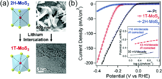
The chemical and electrochemical intercalation can tune the electronic structures of 2D TMDs, thus radically enhancing their chemical and physical reactivity for catalytic applications. Electrochemical intercalation can effectively shift the chemical potentials of 2D TMDs within a wide range, which is suitable for optimizing catalytic properties.61 For example, Li+ intercalated 2D MoS2 has exhibited an enhanced hydrogen evolution reaction (HER).29,62,63 In these cases, intercalated Li atoms transfer excess charge carriers to MoS2, which increases its charge carrier density, and thus its conductivity.29,61 Also, structural phase transitions into more stable octahedral coordination occur to lower the electronic energy of the whole system.29,61 Consequently, the chemical potential of Li-intercalated MoS2 shifts and HER performance is improved. In addition to the alteration of electronic structures, intercalations often alter the structural phases of 2D TMDs to be more suitable for catalysts.25,59,64 For example, electrochemical intercalation of Li+ has been shown to transform the 2H (semiconducting) phase of 2D MoS2 and WS2 into the 1T (metallic) phase, and such 1T-rich 2D TMDs have exhibited enhanced HER performance.25,59,60Fig. 5(a) illustrates a schematic for the 2H-to-1T phase-transition of 2D MoS2 upon Li+ intercalation. The improved catalytic activity is attributed to the following two factors which are results of the phase transition; (1) enhanced charge carrier conductivity due to enhanced metallic phases (2) lowering of the reaction free energy from the release of strain in 1T which is built up from the phase transition. Such a 2H-to-1T phase-transition was also observed in the intercalation of MoS2 where organic molecules such as n-butyllithium intercalants were used.62Fig. 5(b) shows an enhanced HER performance of 1T-rich MoS2 over 2H-rich MoS2 after intercalation with n-butyllithium. Moreover, MoS2 anode electrodes with high capacity and stability were prepared by intercalation and exfoliation restacking processes.65 Intercalations have also been demonstrated to enhance the catalytic activities of 2D TMD-based composite materials. For example, Xiao et al. reported MoS2/polyethylene oxide nanocomposite anodes using exfoliated MoS2 and demonstrated improved lithiation capacity and cyclic performance.66 Liu et al. reported that CdS/MoS2 hybrids obtained using hydrothermal reaction synthesized 1T phase MoS2 showed a giant enhancement of the photocatalytic hydrogen evolution rate.67
 |
| | Fig. 5 (a) Schematic for the transition of the 2H phase to the 1T phase in MoS2 upon Li+ intercalation. (b) Enhanced catalytic performance of 1T MoS2 over 2H MoS2. (from ref. 62). | |
3.2.2. Electrical and optical properties.
Intercalation into layered structures can change the electrical and optical properties of hosting 2D materials. Earlier studies focused on the bulk forms of TMDs are recently revisited as their nanoscale counterparts are now extensively being developed.14 Intercalation can introduce charge transfers in 2D TMDs. For example, 2D TMDs intercalated with transition metals and alkali metals have exhibited electrical properties greatly different from their pristine forms.61 The charge transfer from the metal intercalation shifts the Fermi energy and increases the density of energy states at the Fermi level, thus increasing the charge carrier density of 2D TMDs.61 Metal intercalation also modifies the optical properties of hosting 2D materials. This is manifested by the change of optical transmission and interference, as in the case of Cu-intercalated chalcogenide nanomaterials. Pristine Bi2Se3 nanoribbons display silvery white color which turns orange upon intercalation of Cu.54 The intercalation of Bi2Se3 nanoribbons with organic molecules such as pyridine also results in significant dielectric optical mode peak shifts.68 In addition, Cu-intercalated, very thin 2D Bi2Se3 exhibits unusual enhancement of optical transmission and electrical conductivities.69Fig. 6 shows the enhanced optical transparency ((a) and (b)) and electrical conductivity ((c) and (d)) of 2D Bi2Se3 plates with varying layer thickness upon Cu intercalation. Li+ intercalated, few-layered graphene also displays significantly enhanced optical transmittance and electrical conductance.70 Such an enhanced optical transparency is attributed to the increase of the effective bandgap due to the increase of free electron density introduced by metal atoms.69 In addition to the charge carrier transfer, intercalations can be applied to modulate the physical dimensions of van der Waals interlayer gaps in 2D TMDs. Such a change in the physical structures of 2D TMDs, in turn, results in alteration of their electrical and optical properties. For example, the intercalations of organic molecules have been known to significantly enlarge the interlayer spacing of layered materials in bulk forms.17 This results in the weakening of the bonding strength of 2D interlayers, thus making them electrically behave more like isolated single layers. A similar behavior was observed in the electrochemical intercalation of Li+ into 2D MoS2.29Fig. 7 shows the gradual change of the interlayer spacing in vertically aligned 2D MoS2 upon Li+ intercalation. The ability to externally modulate the electronic structures of 2D TMDs via such simple intercalation may open up substantially novel electrical and optical applications.
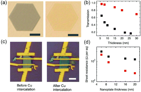 |
| | Fig. 6 (a and b) Tuning the optical properties of Bi2Se3 nanoplates via Cu intercalation. (a) Optical transmission image of an 8 nm thick Bi2Se3 nanoplates before (left) and after (right) Cu intercalations. Scale bar, 4 μm. (b) Optical transmission spectra of Bi2Se3 nanoplates with various thicknesses before (black) and after (red) Cu intercalations. (c and d) Tuning the electrical properties of Bi2Se3 nanoplates via Cu intercalation. (c) A Bi2Se3 nanoplate-based four-point probe measurement device on silicon substrate. Scale bar, 5 μm. (d) Sheet resistance of Bi2Se3 nanoplates with various thicknesses before (black) and after (red) Cu intercalations. (from ref. 69). | |
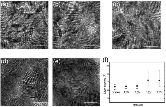 |
| | Fig. 7 Li+ intercalation driven-change of 2D MoS2 interlayer spacing. (a–e) TEM images of MoS2 with 2D molecular layers perpendicular to the substrate (a) before intercalation. (b–e) after intercalation to 1.8, 1.5, 1.2, and 1.1 V vs. Li+/Li, respectively. (f) Averaged layer spacing of pristine and lithiated MoS2. Scale bar, 10 nm. (from ref. 29). | |
3.2.3 Thermoelectrics and photovoltaics.
Intercalation has also been utilized to make the materials properties of 2D materials suitable for energy conversion applications such as thermoelectrics or photovoltaics. In nanostructured thermoelectric materials, the general strategy to enhance thermoelectricity is to reduce the thermal conductivity while maintaining the electrical conductivity.71 In 2D materials, this can be achieved by incorporating intercalants such as atoms, ions, molecules, and guest 2D layers into the van der Waals gaps of hosting 2D materials to perturb phonon propagation. In layered bulk materials, the intercalation of SnS into TiS2 has been demonstrated to make the SnS–TiS2 superlattice which effectively reduces the transverse sound velocity owing to the enhanced interfaces.72 Recent theory suggests that the intercalation of foreign 2D layers into hosting 2D MoS2 can realize various MoS2-based superlattice structures, effectively modifying their electronic structures.73 Intercalating 2D layers further introduces structural disorder in the crystalline lattice of hosting 2D materials, resulting in efficient phonon localization. For example, electrochemical intercalations of Li+ ions have been demonstrated to effectively modulate the thermal conductivity of lithium cobalt oxide (LiCoO2), a layered crystal commonly used as cathode materials.74 Such control of thermal conductivity can be generalized to various TMDs, stimulating interest in designing novel hetero-structured thermoelectric materials inheriting their intriguing 2D nature.61 In addition to thermoelectrics, intercalation can be employed to tune the materials properties of 2D TMDs to be suitable for photovoltaic applications. Hetero-structured 2D TMD composites such as WS2/carbon-nanotubes and WS2/graphene have been demonstrated by the intercalation-based exfoliation and integration of dissimilar 2D materials.39,75 A considerable photoresponse has been observed in these materials, which is attributed to the efficient charge carrier separation due to the electronic junctions at the interfaces of dissimilar 2D materials. Fig. 8 shows a schematic for the intercalation-based fabrication of WS2/graphene photovoltaic devices (a) and the corresponding photoresponse upon illumination (b).
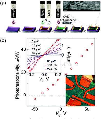 |
| | Fig. 8 (a) Schematic for a fabrication of general heterostructures prepared by using 2D-material solutions. (b) Photoresponsivity of a WS2/graphene device as a function of back gate. (from ref. 75). | |
3.2.4 Magnetic properties and superconductivity.
The Bridgman solid-state reaction, vapor transport and solution reaction intercalations can regulate the magnetic and superconducting properties of 2D TMDs, where the enhanced superconducting critical temperature (Tc) phenomena and a large magneto-resistive effect can be achieved.14,17,76 Intercalated superconducting TMDs can pave a new way for enhancing the c-axis repeat distances to satisfy larger coherence distances of the superconducting wave function than interatomic distances, thus offering a basis for the study of low dimensional superconductivity.14 In bulk layered materials, Geballe et al. reported that the intercalation of n-octadecylamine into TaS2 achieved a large interlayer repeat distance of 5.7 nm, thus forming a large class of new superconductors by varying the certain intercalation molecules and the critical transition temperature can be enhanced to 5.3 K.17 Recently, Clarke et al. reported lithium ions, lithium amide and ammonia intercalation into FeSe forming Lix(NH2)y(NH3)1−yFe2Se2 (x ∼ 0.6; y ∼ 0.2), exhibiting superconductivity at 43 K, higher than in any FeSe-derived compounds except the recent report of FeSe on SrTiO3.77,78 In the past decade, ultrathin 2D materials benefit from intercalation chemistry for many applications. In the case of intercalated topological insulators, enhanced electric conductivity and conversion to superconductors have been observed in the CuxBi2Se3 systems. Fig. 9(a) shows Cu intercalation into the van der Waals gap between Bi2Se3 layers. Transport measurements show superconductivity at 3.8 K in CuxBi2Se3 for 0.12 ≤ x ≤ 0.15 (Fig. 9b). The temperature-dependent resistivity yields an electron concentration (n-type) of ∼2 × 1020 cm−3 (Fig. 9c), an order higher than intrinsic Bi2Se3, which is very different from the non-superconducting Bi2−xCuxSe3 crystals with 0 ≤ x ≤ 0.15.79 Cava et al. also reported that Cu intercalation into TiSe2 induces superconductivity in the range of 0.04 ≤ x ≤ 0.10, proving a first opportunity for the study of charge density waves to superconductivity transition.76 As for the magnetic properties, by proper choice of intercalants, host materials and reaction stage, intercalated compounds can benefit from the spin dimensionality, non-magnetic layers and reduced interplanar magnetic coupling. As shown in Fig. 8d, Morosan et al. reported that Fe can be intercalated into TaS2, forming superlattice diffraction patterns. Fe1/4TaS2 orders ferromagnetically below 160 K and displays very sharp hysteresis loops in the ordered state when magnetic field is parallel to the c axis. For the case of Fe0.28TaS2, Fig. 8e and f show the magnetoresistance measurements of bulk and exfoliated thin-crystals at selected temperatures. The different transition behavior of magnetoresistance curves between bulk (broadening) and 2D crystals (sharping) implies that long range coupling between the Fe ions in different layers is weaker in the 2D crystals. A remarkably large field-perpendicular-to-plane magnetoresistance (MR) exceeding 60% at 2 K was confirmed by anomalous Hall measurements.80,81
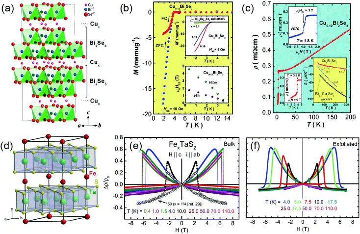 |
| | Fig. 9 (a) Schematic for the crystal structure of Cu intercalated Bi2Se3. (b) The temperature-dependent magnetic transport measurements of a single crystal of Cu0.12Bi2Se3, showing a superconducting transition Tc ∼ 3.8 K from the zero-field-cooled (ZFC) and field-cooled (FC) measurements. (c) The temperature-dependent resistivity of a Cu0.12Bi2Se3 crystal with applied current in the ab plane. (from ref. 79) (d) Schematic for Schematic for the crystal structure of Fe1/4 TaS2. (e and f) Magnetoresistance measurements of bulk and exfoliated thin Fe0.28TaS2 crystals at selected temperatures for H∥c axis, and i∥ab-plane (from ref. 80 and 81). | |
4. Outlook/perspective
In this Review, we have outlined that different strategies of intercalation chemistry pave an efficient way to the production of monolayer or few layer 2D TMDs, modulation of its crystal and band structure and tuning the physical and chemical properties of 2D TMDs. For the synthesis, the remaining challenges are improvement of crystal size, quality and mass production strategies with uniform physical and chemical properties, which can satisfy high performance electronic, optoelectronic, electrochemical catalyst and battery, and biological applications.82 For the physical properties, the intercalation reaction stage and intercalant species should give more rational designs for controlling the band structure, Fermi level and carrier density, for optimizing the superconducting temperature and for inducing magnetic properties. There is no doubt that intercalation chemistry still has extensive space for 2D layered materials researchers toward the study of high-quality new materials,83,84 energy conversion devices and various physical, chemical, and biological properties.
Acknowledgements
J. J. C. acknowledges support from NSF MRSEC DMR 1119826. Y. Z. acknowledges support from NSF DMR 1402600. Y. J. acknowledges the startup fund from the University of Central Florida. All authors contributed to the manuscript.
References
-
S. M. Auerbach, K. A. Carrado and P. K. Dutta, Handbook of layered materials, CRC Press, 2004 Search PubMed.
- P. R. Wallace, Phys. Rev., 1947, 71, 622–634 CrossRef CAS.
- R. W. Keyes, Phys. Rev., 1953, 92, 580–584 CrossRef CAS.
-
N. C. Norman, Chemistry of arsenic, antimony and bismuth, Springer Science & Business Media, 1998 Search PubMed.
-
P. S. Braterman, Z. P. Xu and F. Yarberry, Handbook of layered materials, 2004, 373–474 Search PubMed.
- C. H. Lee, T. Schiros, E. J. G. Santos, B. Kim, K. G. Yager, S. J. Kang, S. Lee, J. Yu, K. Watanabe, T. Taniguchi, J. Hone, E. Kaxiras, C. Nuckolls and P. Kim, Adv. Mater., 2014, 26, 2812–2817 CrossRef CAS PubMed.
- D. W. He, Y. A. Zhang, Q. S. Wu, R. Xu, H. Y. Nan, J. F. Liu, J. J. Yao, Z. L. Wang, S. J. Yuan, Y. Li, Y. Shi, J. L. Wang, Z. H. Ni, L. He, F. Miao, F. Q. Song, H. X. Xu, K. Watanabe, T. Taniguchi, J. B. Xu and X. R. Wang, Nat. Commun., 2014, 5, 5162 CrossRef CAS PubMed.
- M. Chhowalla, H. S. Shin, G. Eda, L. J. Li, K. P. Loh and H. Zhang, Nat. Chem., 2013, 5, 263–275 CrossRef PubMed.
- J. J. Cha and Y. Cui, Nat. Nanotechnol., 2012, 7, 85–86 CrossRef CAS PubMed.
- H. L. Peng, K. J. Lai, D. S. Kong, S. Meister, Y. L. Chen, X. L. Qi, S. C. Zhang, Z. X. Shen and Y. Cui, Nat. Mater., 2010, 9, 225–229 CAS.
- Y. H. Li, J. L. Huang and C. M. Lieber, Phys. Rev. Lett., 1992, 68, 3240–3243 CrossRef CAS PubMed.
- M. Chhowalla, Z. F. Liu and H. Zhang, Chem. Soc. Rev., 2015, 44, 2584–2586 RSC.
- H. T. Yuan, H. T. Wang and Y. Cui, Acc. Chem. Res., 2015, 48, 81–90 CrossRef CAS PubMed.
- M. Dresselhaus, MRS Bull., 1987, 12, 24–28 CAS.
- M. S. Dresselhaus, Phys. Today, 2008, 37, 60–68 CrossRef.
- X. Huang, Z. Zeng and H. Zhang, Chem. Soc. Rev., 2013, 42, 1934–1946 RSC.
- F. R. Gamble, J. H. Osiecki, M. Cais and R. Pisharod, Science, 1971, 174, 493 CrossRef CAS PubMed.
- D. E. Prober, M. R. Beasley and R. E. Schwall, Phys. Rev. B: Solid State, 1977, 15, 5245–5261 CrossRef CAS.
- F. Bonaccorso, Z. Sun, T. Hasan and A. C. Ferrari, Nat. Photonics, 2010, 4, 611–622 CrossRef CAS.
- Y. Jung, J. Shen and J. J. Cha, Nano Convergence, 2014, 1, 1–8 CrossRef.
- B. Radisavljevic, A. Radenovic, J. Brivio, V. Giacometti and A. Kis, Nat. Nanotechnol., 2011, 6, 147–150 CrossRef CAS PubMed.
- O. Lopez-Sanchez, D. Lembke, M. Kayci, A. Radenovic and A. Kis, Nat. Nanotechnol., 2013, 8, 497–501 CrossRef CAS PubMed.
- W. Z. Wu, L. Wang, Y. L. Li, F. Zhang, L. Lin, S. M. Niu, D. Chenet, X. Zhang, Y. F. Hao, T. F. Heinz, J. Hone and Z. L. Wang, Nature, 2014, 514, 470 CrossRef CAS PubMed.
- H. Y. Zhu, Y. Wang, J. Xiao, M. Liu, S. M. Xiong, Z. J. Wong, Z. L. Ye, Y. Ye, X. B. Yin and X. Zhang, Nat. Nanotechnol., 2015, 10, 151–155 CrossRef CAS PubMed.
- D. Voiry, H. Yamaguchi, J. W. Li, R. Silva, D. C. B. Alves, T. Fujita, M. W. Chen, T. Asefa, V. B. Shenoy, G. Eda and M. Chhowalla, Nat. Mater., 2013, 12, 850–855 CrossRef CAS PubMed.
- K. F. Mak, C. Lee, J. Hone, J. Shan and T. F. Heinz, Phys. Rev. Lett., 2010, 105 Search PubMed.
- T. Cao, G. Wang, W. P. Han, H. Q. Ye, C. R. Zhu, J. R. Shi, Q. Niu, P. H. Tan, E. Wang, B. L. Liu and J. Feng, Nat. Commun., 2012, 3, 887 CrossRef PubMed.
- K. F. Mak, K. L. He, J. Shan and T. F. Heinz, Nat. Nanotechnol., 2012, 7, 494–498 CrossRef CAS PubMed.
- H. T. Wang, Z. Y. Lu, S. C. Xu, D. S. Kong, J. J. Cha, G. Y. Zheng, P. C. Hsu, K. Yan, D. Bradshaw, F. B. Prinz and Y. Cui, Proc. Natl. Acad. Sci. U. S. A., 2013, 110, 19701–19706 CrossRef CAS PubMed.
- D. S. Kong, H. T. Wang, J. J. Cha, M. Pasta, K. J. Koski, J. Yao and Y. Cui, Nano Lett., 2013, 13, 1341–1347 CrossRef CAS PubMed.
- Y. Jung, J. Shen, Y. Sun and J. J. Cha, ACS Nano, 2014, 8, 9550–9557 CrossRef CAS PubMed.
- Y. Jung, J. Shen, Y. Liu, J. M. Woods, Y. Sun and J. J. Cha, Nano Lett., 2014, 14, 6842–6849 CrossRef CAS PubMed.
- T. Georgiou, R. Jalil, B. D. Belle, L. Britnell, R. V. Gorbachev, S. V. Morozov, Y.-J. Kim, A. Gholinia, S. J. Haigh and O. Makarovsky, Nat. Nanotechnol., 2013, 8, 100–103 CrossRef CAS PubMed.
- L. Britnell, R. M. Ribeiro, A. Eckmann, R. Jalil, B. D. Belle, A. Mishchenko, Y. J. Kim, R. V. Gorbachev, T. Georgiou, S. V. Morozov, A. N. Grigorenko, A. K. Geim, C. Casiraghi, A. H. Castro Neto and K. S. Novoselov, Science, 2013, 340, 1311–1314 CrossRef CAS PubMed.
- M. M. Furchi, A. Pospischil, F. Libisch, J. Burgdorfer and T. Mueller, Nano Lett., 2014, 14, 4785–4791 CrossRef CAS PubMed.
- J. S. Ross, P. Klement, A. M. Jones, N. J. Ghimire, J. Q. Yan, D. G. Mandrus, T. Taniguchi, K. Watanabe, K. Kitamura, W. Yao, D. H. Cobden and X. D. Xu, Nat. Nanotechnol., 2014, 9, 268–272 CrossRef CAS PubMed.
- C. M. Huang, S. F. Wu, A. M. Sanchez, J. J. P. Peters, R. Beanland, J. S. Ross, P. Rivera, W. Yao, D. H. Cobden and X. D. Xu, Nat. Mater., 2014, 13, 1096–1101 CrossRef CAS PubMed.
- K. S. Novoselov, A. K. Geim, S. V. Morozov, D. Jiang, Y. Zhang, S. V. Dubonos, I. V. Grigorieva and A. A. Firsov, Science, 2004, 306, 666–669 CrossRef CAS PubMed.
- J. N. Coleman, M. Lotya, A. O'Neill, S. D. Bergin, P. J. King, U. Khan, K. Young, A. Gaucher, S. De, R. J. Smith, I. V. Shvets, S. K. Arora, G. Stanton, H. Y. Kim, K. Lee, G. T. Kim, G. S. Duesberg, T. Hallam, J. J. Boland, J. J. Wang, J. F. Donegan, J. C. Grunlan, G. Moriarty, A. Shmeliov, R. J. Nicholls, J. M. Perkins, E. M. Grieveson, K. Theuwissen, D. W. McComb, P. D. Nellist and V. Nicolosi, Science, 2011, 331, 568–571 CrossRef CAS PubMed.
- V. Nicolosi, M. Chhowalla, M. G. Kanatzidis, M. S. Strano and J. N. Coleman, Science, 2013, 340, 1420 CrossRef CAS.
- S. Park and R. S. Ruoff, Nat. Nanotechnol., 2009, 4, 217–224 CrossRef CAS PubMed.
- D. A. Dikin, S. Stankovich, E. J. Zimney, R. D. Piner, G. H. B. Dommett, G. Evmenenko, S. T. Nguyen and R. S. Ruoff, Nature, 2007, 448, 457–460 CrossRef CAS PubMed.
- D. R. Dreyer, S. Park, C. W. Bielawski and R. S. Ruoff, Chem. Soc. Rev., 2010, 39, 228–240 RSC.
- M. Osada and T. Sasaki, J. Mater. Chem., 2009, 19, 2503–2511 RSC.
- M. M. J. Treacy, S. B. Rice, A. J. Jacobson and J. T. Lewandowski, Chem. Mater., 1990, 2, 279–286 CrossRef CAS.
- C. J. Shih, A. Vijayaraghavan, R. Krishnan, R. Sharma, J. H. Han, M. H. Ham, Z. Jin, S. C. Lin, G. L. C. Paulus, N. F. Reuel, Q. H. Wang, D. Blankschtein and M. S. Strano, Nat. Nanotechnol., 2011, 6, 439–445 CrossRef CAS PubMed.
- G. Eda, H. Yamaguchi, D. Voiry, T. Fujita, M. W. Chen and M. Chhowalla, Nano Lett., 2011, 11, 5111–5116 CrossRef CAS PubMed.
- A. A. Jeffery, C. Nethravathi and M. Rajamathi, J. Phys. Chem. C, 2014, 118, 1386–1396 Search PubMed.
- A. A. Jeffery, C. Nethravathi and M. Rajamathi, RSC Adv., 2015, 5, 51176–51182 RSC.
- Q. Liu, X. L. Li, Z. R. Xiao, Y. Zhou, H. P. Chen, A. Khalil, T. Xiang, J. Q. Xu, W. S. Chu, X. J. Wu, J. L. Yang, C. M. Wang, Y. J. Xiong, C. H. Jin, P. M. Ajayan and L. Song, Adv. Mater., 2015, 27, 4837–4844 CrossRef CAS PubMed.
- J. Zheng, H. Zhang, S. H. Dong, Y. P. Liu, C. T. Nai, H. S. Shin, H. Y. Jeong, B. Liu and K. P. Loh, Nat. Commun., 2014, 5, 2995 Search PubMed.
- K. J. Koski, C. D. Wessells, B. W. Reed, J. J. Cha, D. S. Kong and Y. Cui, J. Am. Chem. Soc., 2012, 134, 13773–13779 CrossRef CAS PubMed.
- J. P. Motter, K. J. Koski and Y. Cui, Chem. Mater., 2014, 26, 2313–2317 CrossRef CAS.
- K. J. Koski, J. J. Cha, B. W. Reed, C. D. Wessells, D. S. Kong and Y. Cui, J. Am. Chem. Soc., 2012, 134, 7584–7587 CrossRef CAS PubMed.
- M. J. Wang and K. J. Koski, ACS Nano, 2015, 9, 3226–3233 CrossRef CAS PubMed.
- K. P. Chen, F. R. Chung, M. J. Wang and K. J. Koski, J. Am. Chem. Soc., 2015, 137, 5431–5437 CrossRef CAS PubMed.
- Z. Y. Zeng, Z. Y. Yin, X. Huang, H. Li, Q. Y. He, G. Lu, F. Boey and H. Zhang, Angew. Chem., Int. Ed., 2011, 50, 11093–11097 CrossRef CAS PubMed.
- H. L. Peng, X. F. Zhang, R. D. Twesten and Y. Cui, Nano Res., 2009, 2, 327–335 CrossRef CAS.
- D. Voiry, M. Salehi, R. Silva, T. Fujita, M. W. Chen, T. Asefa, V. B. Shenoy, G. Eda and M. Chhowalla, Nano Lett., 2013, 13, 6222–6227 CrossRef CAS PubMed.
- R. Kappera, D. Voiry, S. E. Yalcin, B. Branch, G. Gupta, A. D. Mohite and M. Chhowalla, Nat. Mater., 2014, 13, 1128–1134 CrossRef CAS PubMed.
- H. T. Wang, H. T. Yuan, S. S. Hong, Y. B. Li and Y. Cui, Chem. Soc. Rev., 2015, 44, 2664–2680 RSC.
- M. A. Lukowski, A. S. Daniel, F. Meng, A. Forticaux, L. S. Li and S. Jin, J. Am. Chem. Soc., 2013, 135, 10274–10277 CrossRef CAS PubMed.
- H. T. Wang, Z. Y. Lu, D. S. Kong, J. Sun, T. M. Hymel and Y. Cui, ACS Nano, 2014, 8, 4940–4947 CrossRef CAS PubMed.
- Z. Y. Lu, H. T. Wang, D. S. Kong, K. Yan, P. C. Hsu, G. Y. Zheng, H. B. Yao, Z. Liang, X. M. Sun and Y. Cui, Nat. Commun., 2014, 5, 43435 Search PubMed.
- G. D. Du, Z. P. Guo, S. Q. Wang, R. Zeng, Z. X. Chen and H. K. Liu, Chem. Commun., 2010, 46, 1106–1108 RSC.
- J. Xiao, D. W. Choi, L. Cosimbescu, P. Koech, J. Liu and J. P. Lemmon, Chem. Mater., 2010, 22, 4522–4524 CrossRef CAS.
- Q. Liu, X. L. Li, Q. He, A. Khalil, D. B. Liu, T. Xiang, X. J. Wu and L. Song, Small, 2015, 11, 5556–5564 CrossRef CAS PubMed.
- J. J. Cha, K. J. Koski, K. C. Y. Huang, K. X. Wan, W. D. Luo, D. S. Kong, Z. F. Yu, S. H. Fan, M. L. Brongersma and Y. Cui, Nano Lett., 2013, 13, 5913–5918 CrossRef CAS PubMed.
- J. Yao, K. J. Koski, W. D. Luo, J. J. Cha, L. B. Hu, D. S. Kong, V. K. Narasimhan, K. F. Huo and Y. Cui, Nat. Commun., 2014, 5, 5670 CrossRef CAS PubMed.
- W. Z. Bao, J. Y. Wan, X. G. Han, X. H. Cai, H. L. Zhu, D. H. Kim, D. K. Ma, Y. L. Xu, J. N. Munday, H. D. Drew, M. S. Fuhrer and L. B. Hu, Nat. Commun., 2014, 5, 4224 CAS.
- M. S. Dresselhaus, G. Chen, M. Y. Tang, R. G. Yang, H. Lee, D. Z. Wang, Z. F. Ren, J. P. Fleurial and P. Gogna, Adv. Mater., 2007, 19, 1043–1053 CrossRef CAS.
- C. L. Wan, Y. F. Wang, N. Wang, W. Norimatsu, M. Kusunoki and K. Koumoto, J. Electron. Mater., 2011, 40, 1271–1280 CrossRef CAS.
- N. Lu, H. Y. Guo, L. Wang, X. J. Wu and X. C. Zeng, Nanoscale, 2014, 6, 4566–4571 RSC.
- J. Cho, M. D. Losego, H. G. Zhang, H. Kim, J. M. Zuo, I. Petrov, D. G. Cahill and P. V. Braun, Nat. Commun., 2014, 5, 4083 Search PubMed.
- F. Withers, H. Yang, L. Britnell, A. P. Rooney, E. Lewis, A. Felten, C. R. Woods, V. S. Romaguera, T. Georgiou, A. Eckmann, Y. J. Kim, S. G. Yeates, S. J. Haigh, A. K. Geim, K. S. Novoselov and C. Casiraghi, Nano Lett., 2014, 14, 3987–3992 CrossRef CAS PubMed.
- E. Morosan, H. W. Zandbergen, B. S. Dennis, J. W. G. Bos, Y. Onose, T. Klimczuk, A. P. Ramirez, N. P. Ong and R. J. Cava, Nat. Phys., 2006, 2, 544–550 CrossRef CAS.
- M. Burrard-Lucas, D. G. Free, S. J. Sedlmaier, J. D. Wright, S. J. Cassidy, Y. Hara, A. J. Corkett, T. Lancaster, P. J. Baker, S. J. Blundell and S. J. Clarke, Nat. Mater., 2013, 12, 15–19 CrossRef CAS PubMed.
- J. F. Ge, Z. L. Liu, C. H. Liu, C. L. Gao, D. Qian, Q. K. Xue, Y. Liu and J. F. Jia, Nat. Mater., 2015, 14, 285–289 CrossRef CAS PubMed.
- Y. S. Hor, A. J. Williams, J. G. Checkelsky, P. Roushan, J. Seo, Q. Xu, H. W. Zandbergen, A. Yazdani, N. P. Ong and R. J. Cava, Phys. Rev. Lett., 2010, 104, 057001 CrossRef CAS PubMed.
- E. Morosan, H. W. Zandbergen, L. Li, M. Lee, J. G. Checkelsky, M. Heinrich, T. Siegrist, N. P. Ong and R. J. Cava, Phys. Rev. B: Condens. Matter, 2007, 75, 104401 CrossRef.
- W. J. Hardy, C. W. Chen, A. Marcinkova, H. Ji, J. Sinova, D. Natelson and E. Morosan, Phys. Rev. B:Condens. Matter, 2015, 91, 054426 CrossRef.
- Q. Liu, C. Sun, Q. He, A. Khalil, T. Xiang, D. Liu, Y. Zhou, J. Wang and L. Song, Nano Res., 2015, 8, 3982–3991 CrossRef CAS.
- W. W. Xiong, J. W. Miao, K. Q. Ye, Y. Wang, B. Liu and Q. C. Zhang, Angew. Chem., Int. Ed., 2015, 54, 546–550 CAS.
- C. L. Wan, X. K. Gu, F. Dang, T. Itoh, Y. F. Wang, H. Sasaki, M. Kondo, K. Koga, K. Yabuki, G. J. Snyder, R. G. Yang and K. Koumoto, Nat. Mater., 2015, 14, 622–627 CrossRef CAS PubMed.
|
| This journal is © the Partner Organisations 2016 |