
Polyvinylidene fluoride molecules in nanofibers, imaged at atomic scale by aberration corrected electron microscopy†
Dinesh
Lolla
a,
Joseph
Gorse
b,
Christian
Kisielowski
c,
Jiayuan
Miao
d,
Philip L.
Taylor
d,
George G.
Chase
a and
Darrell H.
Reneker
*b
aDepartment of Chemical and Biomolecular Engineering, The University of Akron, Akron, OH 44313, USA
bDepartment of Polymer Science, The University of Akron, Akron, OH 44313, USA. E-mail: reneker@uakron.edu; Tel: +1 330-972-6949
cThe Molecular Foundry and Joint Center for Artificial Photosynthesis, Lawrence Berkeley National Laboratory, One Cyclotron Rd, Berkeley CA 94720, USA
dDepartment of Physics, Case Western Reserve University, Cleveland, OH 44106, USA
First published on 15th September 2015
Abstract
Atomic scale features of polyvinylidene fluoride molecules (PVDF) were observed with aberration corrected transmission electron microscopy. Thin, self-supporting PVDF nanofibers were used to create images that show conformations and relative locations of atoms in segments of polymer molecules, particularly segments near the surface of the nanofiber. Rows of CF2 atomic groups, at 0.25 nm intervals, which marked the paths of segments of the PVDF molecules, were seen. The fact that an electron microscope image of a segment of a PVDF molecule depended upon the particular azimuthal direction, along which the segment was viewed, enabled observation of twist around the molecular axis. The 0.2 nm side-by-side distance between the two fluorine atoms attached to the same carbon atom was clearly resolved. Morphological and chemical changes produced by energetic electrons, ranging from no change to fiber scission, over many orders of magnitude of electrons per unit area, promise quantitative new insights into radiation chemistry. Relative movements of segments of molecules were observed. Promising synergism between high resolution electron microscopy and molecular dynamic modeling was demonstrated. This paper is at the threshold of growing usefulness of electron microscopy to the science and engineering of polymer and other molecules.
Introduction
The observation of the positions of atoms in molecules and other structures, with electrons that have wavelengths much shorter than the lengths of inter-atomic bonds, was a promise of electron microscopy that has required over half a century to be fulfilled. Early electron microscopes were designed to have intense electron beams that quickly disrupted any molecule before its atomic scale structure could be recorded. Electron microscopy of polymer and other molecules was limited by the widely held, but mistaken, belief that molecules were destroyed before useful images could be obtained. Recent advances in microscope design and construction, including aberration corrections, increased detector sensitivity and enlarged data handling capacity are now fulfilling that early promise for molecules. The results described here show conclusively that atomic scale resolution in images of polymer nanofibers and other polymeric structures were observed, in detail that is meaningful in the terms of synthesis chemistry and the useful functions of polymer molecules, with many fewer electrons than are required to produce significant chemical changes in the molecules.High-resolution images, made with a spherical aberration corrected microscope, of polyvinylidene fluoride molecules (PVDF) on self-supported nanofibers are described in this paper. A single molecule, supported alongside a very thin nanofiber of PVDF was the exemplary structure examined in this paper. The extended length of the 10 repeat units examined in detail was about 2.5 nanometers. Images were obtained at electron doses ranging from 20 to 2000 e− Å−2. PVDF has two fluorine atoms, separated by 2 Å, connected to the same carbon atom, in each repeating unit of the polymer. Images of these atoms were resolved.
In earlier work,1 with a conventional electron microscope, not corrected for spherical aberration, images of polyvinylidene fluoride (PVDF) electrospun nanofibers, in which the molecular chains were marked by images of the CF2 groups, regularly spaced at intervals of 2.5 Å were obtained by Zhong et al.2 Doses ranged up to 106 e− Å−2. Morphological changes, including polymer chain scission that thinned and eventually broke the nanofiber were followed. At the highest doses, fluorine atoms were observed with a mass spectrometer, which monitored the gases inside the microscope. Fluorine was not observed at the low electron doses required to make a high-resolution image.
Aberration corrected microscopes produce two-dimensional images that reveal sub-atomic details of the interaction between an incident electron, considered as a wave, and the atoms in a sample. Much more precise information about the atom positions than that delivered by previous microscopes is captured. Presently that information needs augmentation from known molecular or crystalline data to calculate the position, in three dimensions, of every atom in a sample that was thicker than two or three atoms. Interpretation of the available information is presently the subject of many contemporary research efforts.3,4
Polymer nanofibers, often made by electrospinning a solution of entangled polymer molecules are excellent samples for electron microscopy.5,6 Attached over a small hole in a substrate, fibers are free of confusion with atoms in the supporting structure. Nanofibers with diameters of around 7 nm were so thin that in the rare event that a secondary electron was generated, it exited the fiber before it could cause further changes. The diameters of nylon nanofibers containing fewer than 10 molecules in a cross section were observed by Huang et al.8 Ma et al.,1 published electron diffraction patterns from thicker nanofibers in which the PVDF molecules were aligned with the fiber axis and crystallized.
The combination of electron micrographs of proteins with 3 Å resolution with the protein structures known from crystallographic measurements is producing rapid progress in the description of assemblies of proteins into biologically important structures. New results appear frequently.9,10
Nam et al.,11 used aberration corrected electron microscopy to observe the self-assembly, from an aqueous solution, of two peptoid polymers into thin (2.7 nm) two-dimensional crystalline sheets. Periodic amphiphilicity, electrostatic recognition and aromatic interactions directed the assembly. Direct visualization of aligned individual peptoid polymers in the sheet structure was achieved. This further demonstrates the growing usefulness of electron microscopy in the examination of biological molecules and molecular nanostructures.12,13
PVDF molecules
PVDF molecules are composed of alternating CF2 and CH2 groups. The molecular weight of the PVDF sample used was 534![[thin space (1/6-em)]](https://www.rsc.org/images/entities/char_2009.gif) 000 grams per mole. The molecular weight, of the CF2–CH2 repeat unit, was 64 grams per mole, so there were 8340 repeat units in a typical molecule. The length of each repeat unit was 0.25 nm. The centers, of the two fluorine atoms attached to the same carbon atom, were separated by about 0.2 nm. The total length of an average molecule was about 2000 nm. The molecular segment examined in detail here was only 0.5% of the length of a typical PVDF molecule. Observation of this single short segment in a conformation achievable with only changes in the dihedral angles, indicated that high-resolution images of a polymer molecule were obtained well before electron induced changes in the molecular bonds occurred.
000 grams per mole. The molecular weight, of the CF2–CH2 repeat unit, was 64 grams per mole, so there were 8340 repeat units in a typical molecule. The length of each repeat unit was 0.25 nm. The centers, of the two fluorine atoms attached to the same carbon atom, were separated by about 0.2 nm. The total length of an average molecule was about 2000 nm. The molecular segment examined in detail here was only 0.5% of the length of a typical PVDF molecule. Observation of this single short segment in a conformation achievable with only changes in the dihedral angles, indicated that high-resolution images of a polymer molecule were obtained well before electron induced changes in the molecular bonds occurred.
In the beta crystalline structure, each PVDF molecule is a planar zigzag of carbon atoms, with fluorine atoms on one edge of the zigzag and hydrogen atoms on the other (see crystallographic information in ESI 6†). A permanent electric dipole, perpendicular to the axis, contributes to strong ferroelectric and piezoelectric effects. Twisting around the long axis and changes in the dihedral angles at carbon–carbon bonds provide mechanisms that change the length of a planar zigzag, as well as the magnitude and the direction of dipole moments of the PVDF molecules. An external electric field applied in a direction perpendicular to the molecular axis acts to change the pattern of multiple twists in a PVDF molecule.14 Twist around the long axis of the molecule, in a polymer segment with a planar zigzag conformation, shortens the length of the segment. Such mechanisms provide electro-mechanical coupling between the applied electric field and the conformation of a molecule.15 Guan et al.,16 measured the integrated effects, of sample preparation methods that could change segmental conformations, on the piezoelectric properties of PVDF and its copolymers.
Preparation of thin nanofibers
Thin nanofibers that support themselves over a hole are advantageous samples that eliminate superimposed images of atoms in any support structure. A 1% solution, of PVDF in a mixture of 3% trifluoroacetic acid in dimethyl sulfoxide was heated to 70 °C for one hour to dissolve the polymer. A droplet of the solution was supported on a single wire loop that had a diameter of about 2 mm. A 25000 volt step in electrical potential was applied to the droplet. Many jets were created and the droplet was consumed in a few seconds. The nanofibers produced from these jets were attracted, by the applied electrical potential difference, to a copper electron microscope grid. The grid supported a lacey carbon film that contained many holes with diameters ranging from around one micron to more than 10 microns. Fibers, with a wide range of diameters, were collected.17 A few PVDF fibers with diameters less than about 10 nm were found, self supported over the holes in the lacey film, and were used to make the observations described below.
A thin fiber, chosen for examination at high magnification, is shown at low magnification in the left panel of Fig. 1. The self-supported part of this fiber was about 400 nm long, and was firmly attached at each end to the curved edge of a hole in a lacey carbon film. A higher magnification image of this fiber is shown in the right panel. The red arrows, shown in both panels, indicate the five areas where 10 nm long segments were imaged at high magnification. The imaged areas were separated far enough that examination of one area did not cause radiation damage to an adjacent area.
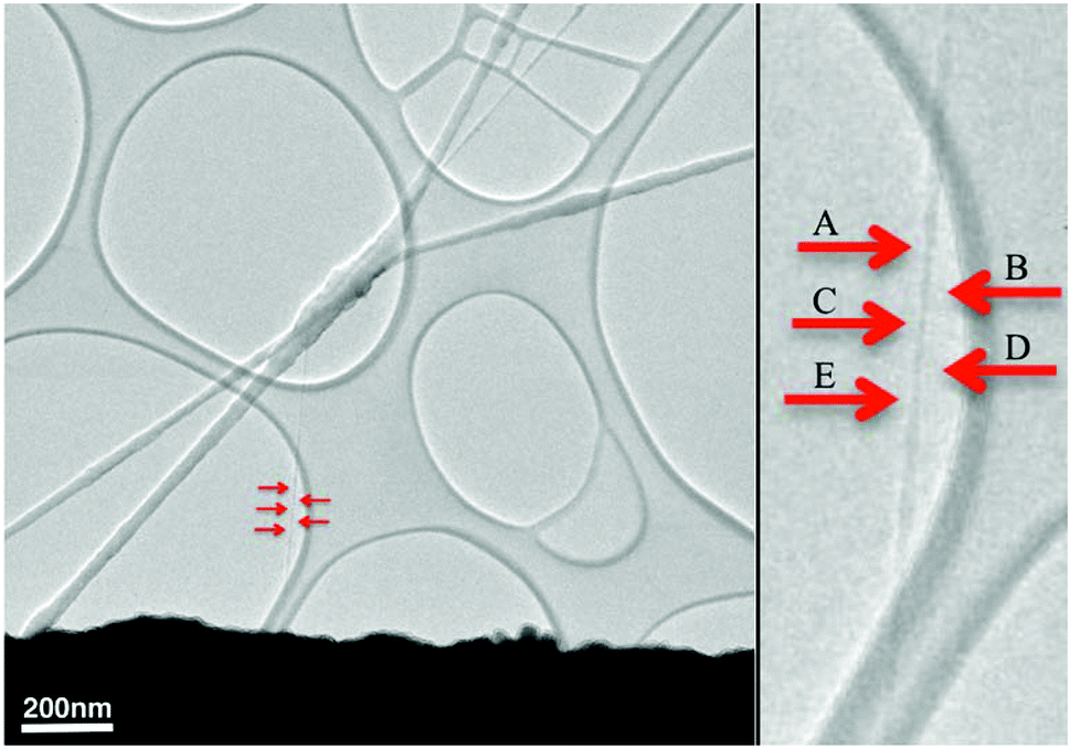 | ||
| Fig. 1 PVDF nanofibers were electrospun onto a lacey film supported by a copper sample grid for a transmission electron microscope. The holes in the lacey film are oval in shape and about one micron across. Zhong2 characterized fibers similar to the larger diameter fibers, which crossed near the center of this image. Searching the grid at low beam intensity revealed the position of several much smaller diameter fibers that were suitable for examination at high resolution. | ||
The diameter of the fiber surrounded by red arrows in Fig. 1 was about 8 nm. The diameter tapered to 3 nm at some places near the middle of the self-supported segment, perhaps in response to capillary forces encountered as the segment dried. The rapid evaporation of the solvent trapped non-crystalline conformations and impeded crystal growth. Examination of a through-focus series of images indicated that the thickness of the fibers was commensurate with their width.4
The wide range of magnifications available in the electron microscope not only recorded molecular scale features but also allowed observations of entire molecules in larger scale assemblies. For example, the relationships between the imaged segments in Fig. 1 and the supporting film, the larger fibers, and even the sample grid are evident. This paper concentrates on a segment of a single molecule in a PVDF nanofiber, with less attention to the many other PVDF molecules in a cross-section of the thin self-supported nanofiber.
Electron microscopy: four strategic steps to high-resolution images
High-resolution micrographs were augmented with other information about PVDF molecules to describe the atom positions in a molecular segment that contained 10 repeat units of PVDF. This short molecular segment was attached to a nanofiber made of PVDF molecules.Four strategic steps used in atomic scale microscopy are described briefly here and the implementation of each step is described in following sections.
Step 1. High resolution, two-dimensional images of a segment of a PVDF molecule were obtained.
Step 2. The images from the transmission electron microscope were combined with relevant information about the chemical structure and conformations to specify the positions of the atoms in a trial model of a particular segment of a PVDF molecule in a particular nanofiber. Examples are listed:
• Structural parameters from chemistry and crystallography of PVDF were used. Images projected into a plane, of the location of the fluorine atoms, provided information about conformations of the molecules.
• Known atom positions in simple conformations of polymer molecules with a planar zigzag of carbon atoms, along with information from the crystallography of PVDF were used to calculate “iconic images” that were recognizable in the micrographs, such as linear rows of CF2 groups, or different iconic patterns of fluorine and carbon atoms seen from different azimuthal directions.
• A three dimensional molecular model, in which dihedral angles at carbon–carbon bonds were adjustable, was used, first to fit the conformation of the model to the positions of CF2 images in the electron micrograph, and then to measure the fitted dihedral angles at every carbon–carbon bond. The spatial coordinates of the atoms in the segment were then calculated.
Step 3. The atom positions in the trial model were used to calculate a simulated image based on the settings and specifications of the microscope.
Step 4. The resulting simulated image was compared with the images from the TEAM 0.5 microscope. Achievement of satisfactory agreement between the microscope image of the segment and the simulated image showed that the trial model was among the best achievable representations of the atom positions in that particular segment of that particular polyvinylidene fluoride molecule.
The high-resolution electron microscope images of thin fibers
The data presented in this paper were obtained with the TEAM 0.5 microscope, with the following operating conditions: spherical aberration (Cs) was set to −15 μm. Accelerating voltage was 80 kV with a variability of 100 meV, focus spread was 0.6 nm, the 5th order spherical aberration (C5), was 5 mm, and chromatic aberration (Cc) was 0.7 mm. Beam divergence was 0.1 mrad. All the images in this paper were produced by the interaction of the exit wave front of electrons that passed through the nanofiber, with a reference wave created by adjustment of the magnitude of the spherical aberration correction. This adjustment was set so that electrons that passed through a fluorine atom, where the electron probability density was high, were whiter in the images. The positions of the fluorine atoms were recognized from the known geometry of PVDF molecules.The image data was captured using a detector with 1024 × 1024 pixels. Each square pixel in the detector corresponded to a square on the polymer molecule that was 0.0236 nm on each edge, at the magnification used. Thus, the electron intensity in a “square Ångstrom” (written Å2) of the molecule was measured at about 18 points, providing a quantitative representation of the electron intensity at a scale commensurate with the length of a chemical bond.
A time series of 101 images were made at intervals of 1 second. The 20 e− Å−2 dose of incident 80 keV electrons required to form a high resolution image almost all passed through the thin fibers without changing any chemical bonds. Only a few small changes in the time series images were evident in a close comparison of the first (20 e− Å−2) and the last (2000 e− Å−2) image of a typical time series.
Successive through focus images were recorded during 0.5 second exposures at a dose rate of 40 electrons per Å2 per second. A defocus step size of 0.5 nm was used. Care was taken to limit the exposure of the sample to the electron beam before recording began.
The observation of thin nanofiber morphology and dose measurements over as many as six orders of magnitude provided new quantitative information relevant to radiation chemistry of polymer molecules. A total dose of around 106 e− Å−2 was required to sever enough bonds to cause an eight nm diameter fiber to thin and break. Zhong,2 observed fibers that broke only after over 2 million e− Å−2, and also made electron energy loss measurements. Lovinger15,18 observed the disappearance of electron diffraction spots from chain folded crystals of PVDF at a dose of 670 e− Å−2 in a sample in which an evaporated coating of carbon and lead (82 electrons per atom) was used to increase contrast. The lead tended to create more secondary radiation events and might thereby have made the PVDF appear to be more sensitive to radiation damage. See further discussion of electron doses in the ESI 9.†
The images, in Fig. 2, of the thin fibers marked with red arrows in Fig. 1, showed many examples of complex, partly ordered but non-crystallographic packing of the molecules. The curved segments of single PVDF molecules contained 10 or 20 repeat units that were supported at occasional contacts with the fiber surface. The positions of the atoms in such a segment of a single molecule were determined with the strategies and methods described above.
 | ||
| Fig. 2 An 18 nm long segment of a PVDF nanofiber is shown in A. The area shown in D was immediately below that shown in A. The diffraction pattern shown in B was a Fourier transform of image D. The filter mask in C was used for the inverse Fourier transform that produced image E. The filter mask was chosen to include the weak diffraction spots in B, to remove sub-atomic details, and to accent the regions shown in E that were weakly aligned parallel to a line from lower left to upper right. (See ESI 2, Video 1†). | ||
Molecular segments of PVDF molecules, five to eight nm long, dominate the image in Fig. 2. This and other such fibers all showed rows of grey to white dots, separated by short distances, that marked a segment of a molecule. The maximum value of this distance (0.25 nm) is known from the chemical structure of PVDF and its beta phase crystallography. Shorter distances were observed when the vector direction of a particular distance between atoms was not perpendicular to the view direction. Where two or more side-by-side molecular segments were observed, their center-to-center distance varied around the ∼0.42 nm distance between adjacent PVDF molecules in a beta phase crystal. Curved and bent segments were also seen in the central part of fiber image, but the details of the superimposed 5 to 10 layers of molecules complicated those images. While significant relative motion of segments within the sample was observed during the time required to collect a complete series of images, such motion was negligible during the time used for a single image.
Fourier transforms of the image data, Fig. 2B, produced diffraction patterns that showed only vestiges of diffraction from crystals. The intensity of the diffraction spots that showed the lateral spacing of side-by-side molecules, and the diffraction spots associated with the 0.25 nm spacing of the fluorine atoms along the molecule were weak and diffuse.
High-resolution micrographs of a segment of a PVDF molecule (Step 1)
Fig. 3 shows a high-resolution image of a short length of a PVDF nanofiber from the sample described in Fig. 1. The axis of this irregular fiber wandered near the vertical direction of the figure. There were several quite complicated layers of molecular segments in the central part of this fiber. Observed changes in the images during observation were minor and attributable to thermal relaxation of conformations, the accumulation of a few radiation events, and small nearly random shifts of the entire image.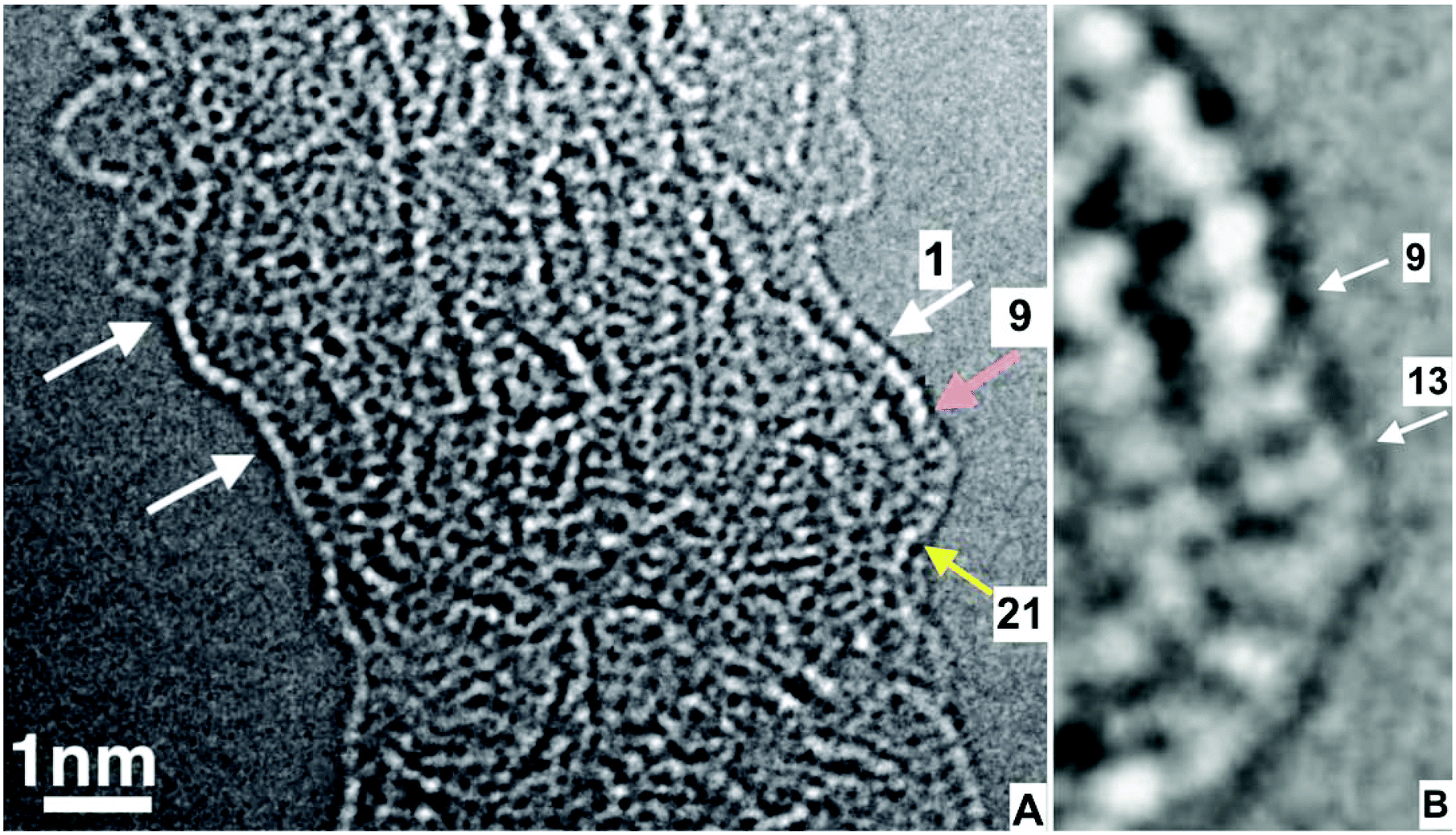 | ||
| Fig. 3 (A) A high resolution transmission electron microscope image of a thin nanofiber of PVDF, (B) is a magnification of part of (A). This micrograph was the 78th of 101 images made in a through-focus series with focus steps of 0.5 nm. This image was recorded with 20 e− Å−2 after a total dose of 1700 e− Å−2 was used to make the preceding 77 images. The defocus chosen to convert the phase information in the microscope to black and white contrast in the image was about 1 nm from the focal setting at which the image contrast disappeared. The molecular segment between the white and yellow arrow was examined in atomic detail in the following text. (Also, see ESI 2, Video 2†). | ||
The brightest dots were attributed to view directions along a line between two fluorine atoms that were attached to the same carbon atom. Rows of such images were abundant. The known 0.25 nm spacing of the CF2 groups along a PVDF molecule provided an internal calibration of the magnification. Rows of such white spots were icons for an essentially planar zigzag conformation of a segment of a PVDF molecule. These rows of dots also helped to identify the locations of projections of CF2 groups onto the image plane in a way that reduced confusion from defocusing artifacts. Many rows of white dots, such as the row at the left in Fig. 3, marked with two arrows, and another on the right, marked with three arrows, were seen in images of this fiber. The segment between the white and yellow arrows protruded far enough that the images of about ten adjacent CF2–CH2 repeat units were not mixed with the image of other molecules in the fiber. The repeat units of interest were numbered in the following way. All the carbon atoms in the observed segment were numbered consecutively. Odd numbers were assigned to the CF2 groups. Each CF2–CH2 repeat unit was identified with the same odd number that was assigned to its CF2 group. The CH2 groups were given even numbers.
In Fig. 3A, a white arrow left, the white arrow points to the repeat unit numbered 1. The pink arrow points to repeat unit 9, which is at the end of the row of dots. The yellow arrow points to repeat unit 23, near where the segment was attached to the fiber. A gradual 80° turn of the molecule, as viewed in the plane of the figure, occurred in repeat units between 13 and 19. At repeat unit 9, the row of bright dots ended, and repeat units 11 and 13 each showed two dimmer, separated spots.
The combination of molecular conformation, molecular bond geometry and electron micrographs to determine 3-D locations of atoms in a trial model of the molecule segment. (Step 2)
The electron micrograph showed the location of the fluorine atoms, in this thin molecular segment, projected in a direction parallel to the view direction of the microscope into the image plane.A flexible model, computed or mechanical, was made of a segment of a PVDF molecule in which all the bond angles, lengths, and relative positions of adjacent fluorine, hydrogen, and carbon atoms were fixed, but the dihedral angles around carbon–carbon bonds in the zig-zag backbone were adjustable. In this 10 repeat unit segment, the 20 dihedral angles were adjusted to the values required for the projected positions of all the fluorine atoms to be at their observed position in the high resolution micrograph shown in Fig. 3. Simultaneously the constraints of the tetrahedral chemical bonds in the molecule were met.7 Short planar zigzag segments of the molecule were joined by short, complicated sequences of a few dihedral angles.
The dihedral angles at each carbon–carbon bond were adjusted and re-adjusted until the fluorine atoms were all at or above an appropriate image. The images of the pairs of fluorine atoms ranged from a bright dot to dimmer side-by-side dots as the amount of twist varied along the segment. These non-circular images were helpful in guiding the adjustment of the dihedral angles in the trial model. In this segment, all the repeating units were near the image plane. The view direction was perpendicular to this zigzag plane.
The electron micrographs provide little information about the positions of atoms in the direction parallel to the view direction. That component, of atomic positions was determined by the structure, in three dimensions, of the PVDF molecule after the dihedral angles were adjusted. A second image of the same segment from a different view direction would produce most of the information needed, but the methods and apparatus for stereographic images, widely used at lower magnification, are not developed for use at the high resolution of the images in this paper. This is a pervasive contemporary problem, presently solved only in a few special cases that do not appear to be helpful here.3,19 Direct measurements of the three-dimensional positions of atoms in molecular conformations above or below the image plane await new tools for measuring the distances, along the view direction, between each atom and the image plane.
The trial model, shown in Fig. 4B, was calculated from the list of dihedral angles generated in fitting the flexible zigzag model to the atom locations revealed in the micrograph. The list of dihedral angles for this segment is included in the ESI.† The uncertainty in the measurement of the dihedral angles in the fitted model was about ±10 degrees, so small deviations in the dihedral angles of the trial model were not precisely represented.
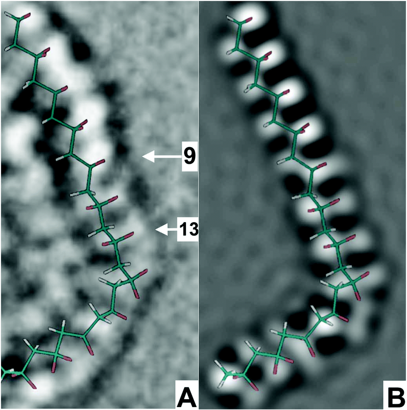 | ||
| Fig. 4 (A). An enlarged copy of the segment marked with three arrows in Fig. 3, (B) is the computed simulation of the trial model. The trial model is represented by the overlaid stick figure in which the carbon–carbon bonds are green, the CH2 groups are white, and the CF2 groups are red. (Also, see ESI 1† for dihedral angles of trial model, ESI 2 for Video2† for 101 images of through focal series and video 4† is 3D molecular dynamics trial model). | ||
Calculated image of the trial model (Step 3)
The image of the trial model was calculated, using a microscope-emulating program SimulaTEM that approximated the aberrations and settings of the real microscope.20 This program produced simulated images from the coordinates of all the atoms of the trial model, assuming that all the bond lengths and bond angles in the repeat units molecule did not change. For repeat units 3 to 21, Fig. 4A, B were in good agreement, so the trial model was considered to be a close representation of the molecular segment.While many polymers form regular crystals, these PVDF fibers did not, because solidification from the thin jet of PVDF solution was too rapid.21 Methods developed for interpreting three dimensional crystals containing defects are of limited applicability19 to these fibers. Instead, methods that utilized the presence of fluorine atoms, with 9 electrons, in a polymer chain with a well-established chemical structure, were used. The positions of carbon atoms, with 6 electrons, were shown in the calculations.
Comparison of the image calculated from the trial model with the electron micrograph of the molecule (Step 4)
Fig. 4 shows the comparison of the micrograph, the trial model deduced from the micrograph and other information about the molecule, and the image simulated from the atom positions in the trial model. The micrograph showed repeat units to 1 to 7 as a row of bright dots indicating a nearly planar zigzag. The bright dot, at repeat unit 9, was followed with two side-by-side gray dots (a capsule shape) at repeat units 11 and 13. This iconic image indicated that the PVDF molecule was twisted around its axis by about 90° and viewed from a direction perpendicular to the zigzag plane defined by the row of white dots associated with repeat units 1 to 7.The sudden change in appearance, between repeat units 9 and 11, was associated with changes in several nearby dihedral angles, which introduced about 90° of twist around the molecular axis. This twist changed the local view direction and presented a dimmer, side-by-side, capsule shaped image of the two fluorine atoms attached to the same carbon atom.
This twisted and bent molecular segment was close to a plane defined by the planar zigzag formed by the repeat units 3 to 7. At the CH2 group 8, in repeat unit 7, the zigzag began to twist around the long axis of the preceding segments. Repeat units 11 and 13 defined a short planar zigzag that was rotated about 90° so that the two fluorine atoms on each of these repeat units were viewed from a direction nearly perpendicular to the line between their fluorine atoms (the capsule view). At repeat units 15, 17, and 19, the segment bent about 80° in the plane and also untwisted so the segments which followed formed a planar zigzag that defined plane nearly parallel to that defined by repeat units 1 to 7.
This change in the image of a PVDF molecule provided an icon that marked the presence of about 90° of twist around the long axis of the molecule. The two fluorine atoms on a particular carbon atom, which are separated by less than 2 Å, were clearly resolved. Twist in the PVDF molecule provides an interesting mechanism for changing the direction of the electrical dipole moment of a molecular segment. Reneker and Mazur22 described other related geometrical features of twisting and bending in a planar zigzag molecule of polyethylene in a folded chain crystal.
The four dimmer spots (two spots at repeat units 11, and two spots at repeat unit 13) are each attributed to a single fluorine atom. The left to right separation of the pairs of fluorine atoms is know from the molecular structure to be near 2 Å. The spacing of the fluorine atoms along the molecule is near 2.5 Å. All these distances are clearly resolved in Fig. 5. The right to left separation of both pairs of dots is less than the vertical separation of the spots in repeat units 11 and 13.
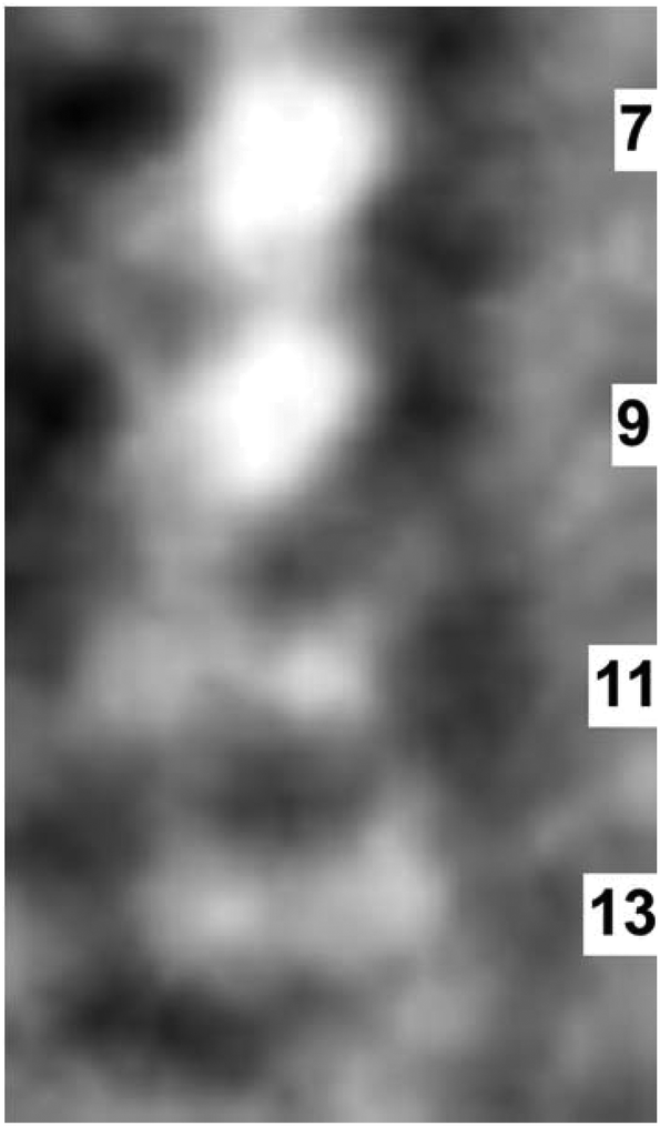 | ||
| Fig. 5 An enlarged micrograph of repeat units 7, 9, 11, and 13 as they appeared in the data in Fig. 3. | ||
Synergism of high-resolution electron microscopy and molecular dynamical modeling
Molecular dynamics calculations produced models of realistic molecular conformations inside a thin fiber. The positions of the atoms and molecules in three dimensions were calculated and the appearance of a twisted PVDF molecule in an electron micrograph was calculated and used to recognize the presence of twist.Removing all the other molecules revealed the molecular path followed by a particular segment of a molecule inside a nanofiber. After molecular dynamics calculations simulating annealing of a PVDF nanofiber at 300 K for 500 picoseconds, the twisted and curved molecule shown in Fig. 6B was found. This observation shows that twisted conformations, almost as complicated as those described in a molecular segment attached to the free surface of a nanofiber, were likely to occur inside the nanofiber during thermal annealing. The creation and motion of such conformations inside thicker PDF samples involve many cooperative rearrangements of adjacent molecules. The coupling between an electric field that tended to align the strong electric dipoles associated with the PVDF molecules, and the changes in the external dimensions of a fiber can be investigated in great detail by combining molecular dynamics calculations and high resolution electron microscopy with measurements of piezoelectric effects.
 | ||
| Fig. 6 (A) A stick model of twist created in a molecular segment during a molecular dynamic calculation. (B) A space-filling model of same segment with neighboring molecules. | ||
Summary and conclusions
Observations of molecular structures and mechanisms, such as twist, at the atomic scale provide information relevant to the conception and design of molecular structures that transport ions and electrons in molecular scale logical devices, catalysts, recognition of particular molecular moieties and much more. Presently, spherical aberration corrected electron microscopy, molecular dynamics calculations of atom positions, calculations of electron probability density in molecules, improved, larger and faster direct-detection electron-counting for images in a microscope are providing new tools for the analysis and design of atomic scale devices and structures.This paper shows high-resolution images of atoms and atomic scale features of PVDF in electrospun nanofibers. Quantitative measurements of electron dose and detailed observations of changes in chemical bonds show that many useful images were obtained long before electron-induced changes to molecular scale features became apparent. The goal of observing the position in three dimensions of all the atoms in a representative volume of PVDF was achieved. Fluorine, or other high atomic number atoms at strategic places in a molecule are easily distinguished in the images.
Molecular dynamics calculations of the conformations of polymer molecules, as the molecules diffuse and relax toward lower energy shapes, produce realistic conformations of molecules in which the three dimensional position of all the atoms are known from the calculations. The use of this data to generate stereographic simulated electron microscope images of recognizable features of PVDF molecules was demonstrated. Comparisons of computed images and electron micrographs of segments of molecules are now available at the same atomic scale. Chain scission was produced by electron doses per unit area that were thousands or more times larger than needed for imaging. Molecular dynamic models of molecular relaxation, after chain scission, were modeled and simulated electron microscope images at the atomic scale23 were generated. The dipolar electrical fields associated with twisted molecules in PVDF nanofibers extend outside a PVDF nanofiber in ways that attract and hold very small particles, and are therefore of interest in filtration and separation technology.24–26
Acknowledgements
The authors thank: Coalescence Filtration and Nanofiber Consortium (Ahlstrom, Bekaert, Cummins Filtration, Donaldson, Hollingsworth and Vose, Parker Hannifin, and SNS Nanofiber Technology), for providing financial support; Manideep Lolla for the graphic abstract; Alexander Yarin for insights into electrospinning of very thin fibers; Shing-Chung Wong, Zhenxin Zhong, Bojie Wang, Min Gao, and Alan Nicholls, for electron microscopy; and Mesfin Tsige for molecular modeling.Work at the Molecular Foundry was supported by the Office of Science, Office of Basic Energy Sciences, of the U.S. Department of Energy under Contract No. DE-AC02-05CH11231.
References
- X. Ma, J. Liu, C. Ni, D. C. Martin, D. B. Chase and J. F. Rabolt, ACS Macro Lett., 2012, 1, 428–431 CrossRef CAS
.
- Z. Zhong, J. Y. Howe and D. H. Reneker, Polymer, 2013, 54, 3745–3756 CrossRef CAS
- D. Van Dyck and F.-R. Chen, Nature, 2012, 486, 243–246 CrossRef CAS PubMed
- F.-R. Chen, C. Kisielowski and D. Van Dyck, Micron, 2015, 68, 59–65 CrossRef CAS PubMed
- J. Doshi and D. H. Reneker, Ind. Appl. Soc. Annu. Meet. 1993., Conf. Rec. 1993 IEEE, 1993, vol. 3, pp. 1698–1703.
- D. H. Reneker and A. L. Yarin, Polymer, 2008, 49, 2387–2425 CrossRef CAS
- W. Humphrey, A. Dalke and K. Schulten, J. Mol. Graphics Modell., 1996, 14, 33–38 CrossRef CAS
- C. Huang, S. Chen, C. Lai, D. H. Reneker, H. Qiu, Y. Ye and H. Hou, Nanotechnology, 2006, 17, 1558 CrossRef CAS PubMed
- J. Jiang, B. L. Pentelute, R. J. Collier and Z. H. Zhou, Nature, 2015, 521, 545–549 CrossRef CAS PubMed
- C. Kisielowski, P. Specht, S. M. Gygax, B. Barton, H. A. Calderon, J. H. Kang and R. Cieslinski, Micron, 2015, 68, 186–193 CrossRef CAS PubMed
- K. T. Nam, S. A. Shelby, P. H. Choi, A. B. Marciel, R. Chen, L. Tan, T. K. Chu, R. A. Mesch, B.-C. Lee, M. D. Connolly, C. Kisielowski and R. N. Zuckermann, Nat. Mater., 2010, 9, 454–460 CrossRef CAS PubMed
- M. Haruta and H. Kurata, Sci. Rep., 2012, 2, 2–5 Search PubMed
- D. C. Martin, J. Chen, J. Yang, L. F. Drummy and C. Kübel, J. Polym. Sci., Part B: Polym. Phys., 2005, 43, 1749–1778 CrossRef CAS
- L. Yang, X. Li, E. Allahyarov, P. L. Taylor, Q. M. Zhang and L. Zhu, Polymer, 2013, 54, 1709–1728 CrossRef CAS
- A. J. Lovinger, Sci., 1983, 220, 1115–1121 CAS
- F. Guan, J. Wang, J. Pan, Q. Wang and L. Zhu, Macromolecules, 2010, 43, 6739–6748 CrossRef CAS
- H. U. Shin, Y. Li, A. Paynter, K. Nartetamrongsutt and G. G. Chase, Polymer, 2015, 65, 26–33 CrossRef CAS
- A. J. Lovinger, Macromolecules, 1985, 18, 910–918 CrossRef CAS
- S. J. Haigh, B. Jiang, D. Alloyeau, C. Kisielowski and a. I. Kirkland, Ultramicroscopy, 2013, 133, 26–34 CrossRef CAS PubMed
- A. Gómez-Rodríguez, L. M. Beltrán-del-Río and R. Herrera-Becerra, Ultramicroscopy, 2010, 110, 95–104 CrossRef PubMed
- H. U. Shin, A. B. Stefaniak, N. Stojilovic and G. G. Chase, Environ. Sci. Nano, 2015, 2, 251–261 RSC
- D. H. Reneker, Polymer, 1982, 24, 1387–1400 CrossRef
- J. Miao, R. S. Bhatta, D. H. Reneker, M. Tsige and P. L. Taylor, Polymer, 2014, 56, 482–489 CrossRef
- S. U. Patel, G. M. Manzo, S. U. Patel, P. S. Kulkarni and G. G. Chase, J. Nanotechnol., 2012, 2012, 1–8 CrossRef
- S. U. Patel and G. G. Chase, Sep. Purif. Technol., 2014, 126, 62–68 CrossRef CAS
- G. Viswanadam and G. G. Chase, Sep. Purif. Technol., 2013, 104, 81–88 CrossRef CAS
Footnote |
| † Electronic supplementary information (ESI) available. See DOI: 10.1039/c5nr01619c |
| This journal is © The Royal Society of Chemistry 2016 |