
 Open Access Article
 This Open Access Article is licensed under a
 Creative Commons Attribution 3.0 Unported Licence
Can slow-moving ions explain hysteresis in the current–voltage curves of perovskite solar cells?†
Giles
Richardson
*a,
Simon E. J.
O'Kane
b,
Ralf G.
Niemann
c,
Timo A.
Peltola
b,
Jamie M.
Foster
d,
Petra J.
Cameron
c and
Alison B.
Walker
*b
aMathematical Sciences, University of Southampton, UK
bDepartment of Physics, University of Bath, UK. E-mail: a.b.walker@bath.ac.uk
cDepartment of Chemistry, University of Bath, UK
dDepartment of Mathematics and Statistics, McMaster University, Hamilton, Canada
First published on 12th February 2016
Abstract
The hypothesis that ion motion is responsible for anomalous hysteresis in the current–voltage curves of perovskite solar cells is investigated through a combination of electrical transport modelling and experimental measurements. In a combined computational and experimental study, good agreement is obtained between experiment and the results of a charge transport model covering mixed ionic-electronic conduction. Our model couples electrons, holes and defect mediated ion motion suggesting that slow moving ions are indeed the origin of the hysteresis. The magnitude of the ion diffusion coefficient required to match experiment and theory, ∼10−12 cm2 s−1, depends on the cell, but is similar to that predicted by microscopic theory of vacancy mediated diffusion. The investigation is extended to preconditioning procedures which are known to substantially influence the hysteresis. The method developed for solving the stiff equations in the drift diffusion model is widely applicable to other double layer problems occurring in electrochemical applications such as the evolution of transmembrane potentials in living cells.
Broader contextA perovskite solar cell is so-called because it includes a perovskite structured compound, most commonly a hybrid organic–inorganic lead or tin halide-based material, as the light-harvesting active layer. These cells were mentioned as an exciting development in the climate change conference in Paris in December 2015. The record certified power conversion efficiency for these cells is 21.0%. A well-known problem is hysteresis in which the cell current–voltage characteristics are strongly dependent on the voltage scan rate, direction and pre-conditioning treatments. Despite evidence from cell measurements identifying the likely cause of hysteresis as ion migration, there is no theoretical model capable of interpreting measured current–voltage characteristics that show hysteresis. Here, we report a combined theoretical–experimental investigation of hysteresis where we have identified the physical origin of the features seen in the measurements. Our model takes an approach to solving the charge transport equations that is widely applicable to other double layer problems occurring in electrochemical applications such as the evolution of transmembrane potentials in living cells. The model allows us to understand the effect of mobile defects on the operational mechanisms of the devices and paves the way for the development of cells with improved and reproducible performance. |
1 Introduction
Since the first use of organolead halide perovskites as a sensitizer in a solar cell in 2009,1 the power conversion efficiency, PCE, of perovskite solar cells has risen from 3%2,3 to around 20% within five years. Recent reviews of perovskite solar cells are given by Stranks and Snaith,4 Niu et al.,5 Miyasaka,6 and Park.7Planar perovskite cells are produced by sandwiching a layer of perovskite, such as the compound MAPbI3 (where MA is short for methylammonium, CH3NH3) between electron transporting and hole transporting contacts. The most common combination is titania (TiO2) for the former and spiro, namely spiro-MeOTAD,2,2′7,7′-tetrakis-(N,N-di-p-methoxyphenyl amine)-9,9′-spirobifluorene as the latter.
A major weakness that undermines the credibility of measurements of perovskite solar cell PCEs is the choice of a voltage scanning protocol that takes advantage of hysteresis in the current density–voltage, J–V, curves to obtain apparent efficiencies that are in excess of the real efficiency of the cell. Indeed it was not until 2014, in the work of Snaith et al.,8 and others,9–12 that this source of inaccuracy was openly discussed in the literature. An understanding of the underlying working principles of perovskite cells is crucial to their future improvement,10 not just the PCEs but also to achieve rapid energy payback time and sustainability.13 Ion motion within the perovskite could lead to degradation of the perovskite material as it becomes depleted in I−, and will inevitably lower the PCE of the cell by reducing the built-in electric field in the perovskite. Furthermore, ion motion is not an effect that can be averted by encapsulation.14,15
Snaith et al.8 suggested three origins for hysteresis from the perovskite layer, either solely or in combination: (a) a large defect density close to interfaces with adjacent layers; (b) slow polarization of the material due to bias dependent motion or changes in configuration of the ferroelectric domains;16 (c) vacancy aided migration of ions through the film. Mechanism (a) is unlikely since electronic transport to the layer takes ∼ns due to the high electronic mobility (though we note that charges could detrap on a timescale comparable to that associated with the hysteresis) and mechanism (b) is ruled out by electrical measurements.17 Belstein-Edmands et al.17 provide strong evidence for mechanism (c) estimating that motion of up to 3.7% of I− contributes to the hysteresis. With a measured stored charge density of 2.5 mC cm−2 at 2 V, an ionic capacitance of 0.28 mF is inferred, similar to the low frequency capacitance reported elsewhere.9 Recent work18 has shown that hysteresis can be reduced by replacing the TiO2 layer by PCBM and that this is associated with a reduction in the low frequency capacitance of the cell. Apparent PCEs of 11% and 13% have been measured from the J–V scans of meso-structured cells without a TiO2 blocking layer but the cells have nevertheless been shown to have nearly zero stabilized power output.19 Li et al.15 have shown that by preconditioning similar cells that apparent PCEs increased from less than 1% to over 8% and that this can be attributed to ion motion. O'Regan et al.20 found that that the apparent efficiency of a cell aged for 100 days varied between 0.1% and 9% depending on the time for which the cell was held at forward bias. In addition they were able to identify two distinct contributions to the transient response of the cell one of which (on a microsecond timescale) they ascribe to detrapping of electrons and the other (on the scale of 10 s of seconds) they ascribe to ion motion or dipole realignment. In terms of their capacitances the slow timescale response is much more significant than the fast timescale one.
Yang et al.21 support the hypothesis that hysteresis arises from the motion of I− ions in the perovskite, inferring an ionic diffusion coefficient of 2.4 × 10⁻⁸ cm2 s−1. Atomistic calculations by Eames et al.22 using Density Functional Theory, DFT, methods employing an ab initio code showed the fastest ion motion is vacancy assisted I− diffusion. Here the positively charged I− vacancies are the mobile species rather than the I− ions, with an activation energy EA of 0.58 eV from which a diffusion coefficient D+ ∼ 10−12 cm2 s−1 was deduced at a temperature of 320 K. They postulated that this vacancy migration could help to explain hysteresis. Other ion species that could also explain hysteresis include negatively charged I− interstitials, which would also explain the results of Yang et al.21 and negatively charged MA+ and Pb2+ vacancies. Eames et al.22 calculated EA to be 0.84 eV for MA+ and to be 2.31 eV for Pb2+, leading to corresponding diffusion coefficients of D+ ∼10−16 cm2 s−1 and effectively zero respectively. On the other hand, DFT calculations by Azpiroz et al.23 yielded values of EA of ∼0.16 eV, 0.5 eV and 0.8 eV for I−, MA+ and Pb2+ vacancies, respectively. They suggested that I− vacancies and interstitials move too quickly to be responsible for the hysteresis and therefore MA+ vacancies are a possible cause. However the value of D+ ∼10−4 cm2 s−1 for I− vacancies (inferred from EA = 0.16 eV) is so large that the electric field across the device would be fully compensated before the MA+ vacancies had time to move. In turn this implies that no hysteresis would be observed over the 10 s timescale that characterizes this phenomenon. MA+ and Pb2+ vacancy motion is also inconsistent with the results of Yang et al.21 For both these reasons we can rule out mobile MA+ and Pb2+ vacancies being the cause of the hysteresis.
The large number of results described above that lack a coherent explanation demonstrate that much perovskite research is based on a ‘shake and bake’ approach, uninformed by an understanding of the underlying mechanisms. Given the complexity of the proposed hysteresis mechanisms, a device model is essential and is one of 10 critical challenges posed in a recent review.24 Atomistic models show considerable discrepancies in their predictions of the parameters governing ion motion as shown in the previous paragraph. Furthermore, the use of such models on the length scales required to study charge transport in solar cells is not feasible because of the huge computational cost involved; the appropriate tool for such studies (especially for planar devices) is the drift diffusion, DD, method.25 DD models of coupled ion–electron conduction allow us to understand the effect of mobile ions on the operational mechanism of the device8–12,19,22,23 and pave the way for the development of cells with improved and reproducible performance. The model reported here is a development of the DD model by Foster et al.26 This model has guided developments in cell longevity via an equivalent circuit model that quantified the loss in charge arising from shunting where the metal electrode and the perovskite absorber layer make contact.27
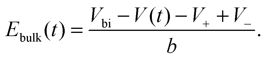
Within our DD picture, a built-in voltage Vbi, determined by the difference in the Fermi levels in the TiO2 and the spiro layers, gives rise to an electric field Vbi/b in the perovskite layer. This field drives positive charges towards the spiro layer and negative charges towards the TiO2. At short circuit, free electron–hole pairs are separated by this field to create a current in which electrons are extracted through the TiO2 layer and holes are extracted through the spiro layer. A positive applied bias, V, produces an electric field that opposes the built-in field. In the absence of charge build up within the perovskite there is a net electric field (Vbi − V)/b from left to right. When V < Vbi, this field drives the positively charged iodide vacancies into the region of the perovskite adjacent to its interface with the spiro, where they create a narrow positively charged layer of total areal charge density Q+. To maintain overall charge neutrality, there is also a negatively charged layer, created by depletion of the iodide vacancies of total areal charge density Q−, in the region of the perovskite adjacent to its interface with the TiO2. Fig. 1 illustrates the resulting electric potential and conduction band profile.
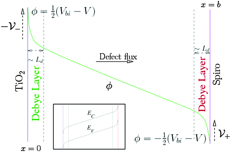 | ||
| Fig. 1 Schematic of the electric potential ϕ in the perovskite. ϕ is linear across most of the perovskite film but varies rapidly across narrow Debye layers at its edges, jumping by an amount V− across the left-hand layer and V+ across the right-hand layer. We assume the applied bias V is zero at short circuit and is positive at the right hand contact relative to the left hand contact. The inset shows the equivalent band energy diagram in the perovskite. EC and EV depend upon ϕ via EC = −Eea −qϕ and EV = −Eea − Eg − qϕ where Eea and Eg are the electron affinity and energy gap, respectively. | ||
The charge accumulation layers, termed Debye layers, are examples of a diffuse double layer, such as seen in electrolytes.28,29 The width of the layers can (as for electrolytes) be estimated from the Debye length LD, which is proportional to the reciprocal of the square root of the density of the mobile charged species. Ab initio theory30 predicts an equilibrium I− vacancy density of 1.6 × 1019 cm−3 and a corresponding Debye length LD ≈ 1.5 nm that is much smaller than the perovskite layer width ≈300 nm. Our approach explicitly accounts for ion motion and predicts charge accumulation in these layers on the time scales associated with mobile defect motion in the perovskite that are consistent with experimental measurements and theoretical estimates of D+. Using the vacancy diffusion coefficient 10−12 cm2 s−1 calculated by Eames et al.22 leads to an estimate of the timescale for vacancy diffusion across a distance 5LD of around 0.5 s which is consistent with experimental observations of hysteresis at scan rates of ∼1 V s−1 from open circuit to short circuit and back.
There are very few published DD models of perovskite cells.31–34 Of these, only Van Reenen et al.34 (published while this work was in review) addresses ion migration. In that work a finite difference based numerical scheme is employed. The constant grid spacing of 4 nm is far too coarse to resolve the Debye layers. Their assumed value of D+ is 106 times greater than that of Eames et al.22 and voltage scan rates around 106 times greater than the experimental scan rates at which hysteresis is observed, ruling out a quantitative comparison with experiment.
Our approach is more sophisticated and involves solving explicitly for the potential and ion distributions in the narrow (and problematic) Debye layers. By comparing our results to experiment, we can deduce the value of D+, finding it to be close to the value of 10−12 cm2 s−1 predicted by Eames et al.22 With additional experimental J–V curves for different device structures and scan rates, our model would help resolve the question whether other mobile species, such as MA+ and Pb2+ vacancies contribute to hysteresis. With a little additional work our model can also be used to address empirical observations showing that cells with fullerene (C60) derivative PCBM, [6,6]-phenyl-C61-butyric acid methyl ester, as an electron transport layer have reduced hysteresis.18 This reduction is especially marked in inverted structures such as ITO/PEDOT:PSS/MAPbI3/PCBM/C60/BCP/Al. Here ITO is Indium Tin Oxide, PEDOT:PSS is poly(3,4-ethylenedioxythiophene) polystyrene sulfonate and BCP is bathocuproine.18,35 The reduction in hysteresis in these devices is also predicted by our model and is the subject of a current study, but is outside the scope of this paper which focuses on the conventional TiO2 and spiro based devices.
It is possible that illumination levels may also influence vacancy concentration. Hoke et al.,36 for example, speculate that photoexcitation may cause halide segregation in mixed halide perovskites resulting in photoinduced trap formation that could influence hysteresis. However, since no clear experimental evidence exists for such effects, we omit them from our model.
To validate our model, we compare its predictions with experimental measurements on two cells chosen to demonstrate high levels of hysteresis. Features seen in the measured J–V curves at varying scan rates, such as a shallow peak on scans from 1.2 V to short circuit, can be explained in terms of a time varying internal electric field across the perovskite layer. These measurements, and their interpretation, are extended to include discussion of the influence of preconditioning. By reporting on the two cells, we show how much J–V characteristics vary for cells fabricated in the same way but with different preconditioning. Validation of our methodology through this comparison opens the way to study other solar cells containing mixed ionic electronic conductor materials, such as CuInSe2 in which Cu+ can migrate.14
2 Methods
Choice of model parameters
Table 1 shows parameter definitions and values adopted in our model. All values are for room temperature, set as 298 K. Values for n0 and p0 were calculated from the effective density of states ĝc, ĝv, the conduction and valence band edges EC and EV and the Fermi levels in the TiO2 and spiro EFt, EFs.| Symbol | Description | Value |
|---|---|---|
| N 0 | I− vacancy equilibrium density | 1.0 × 1017 cm−3Fig. 3, 4 |
| 1.6 × 1019 cm−3Fig. 5–830 | ||
| n 0 | Density of free electrons at TiO2 | 6.9 × 1013 cm−3ref. 37, 38 |
| p 0 | Density of free holes at spiro | 1.0 × 1012 cm−3ref. 37, 38 |
| ĝ c | Conduction band density of states | 8.1 × 1018 cm−3ref. 38 |
| ĝ v | Valence band density of states | 5.8 × 1018 cm−3ref. 38 |
![[D with combining circumflex]](https://www.rsc.org/images/entities/i_char_0044_0302.gif) n
n
|
Electron diffusion coefficient | 1.7 cm2 s−1ref. 39 |
|
p
|
Hole diffusion coefficient | 1.7 cm2 s−1ref. 39 |
| E C | Conduction band minimum | −3.7 eV ref. 37 |
| E V | Valence band maximum | −5.4 eV ref. 37 |
| E Ft | TiO2 Fermi level | −4.0 eV ref. 37 |
| E Fs | Spiro Fermi level | −5.0 eV ref. 37 |
| L d | Debye length = (εpVT/(qN0))1/2 | 1.5 nm |
| b | Perovskite layer width | 6 × 10⁻⁵ cm ref. 39 |
| ε 0 | Vacuum permittivity | 8.85187 × 10⁻¹² F m−1 |
| ε p | Static dielectric constant | 24.1ε0ref. 38 |
| q | Electron charge magnitude | 1.602 × 10⁻¹⁹ C |
| V T | Thermal voltage | 0.0257 V |
| V bi | Built-in voltage | 1 V |
| v scan | Scan rate | See figure caption |
| α | Absorption coefficient | 1.3 × 105 cm−1ref. 40 |
Parameters fit to experiment are shown in Table 2. Our treatment of light absorption via the Beer–Lambert law with a single value for the absorption coefficient is approximate so we have used a value of Fph that gives short circuit current densities in the range 5–15 mA cm−2, reproducing measurements by Sanchez et al.9 and the measurements reported in the Results section. Tress et al.11 find that hysteresis is independent of illumination, motivating our assumption that D+ is similarly independent of illumination despite its soft structure. The perovskite film nanoscale morphology, in the form of its grain boundary structure, influences D+ and accounts for differences between cells fabricated in the same way. Fitting predicted J–V characteristics for varying scan rates to experiment gives an estimate of D+ that differs by a factor of three between the two cells. Our estimates for D1+ and D2+ are both within a factor of 10 of that calculated by Eames et al.22 but are further away from that determined by Yang et al.21
| Symbol | Description | Value |
|---|---|---|
| F ph | Intensity at x = 0 | 9.45 × 1016 cm−2 s−1 |
| D 1+ | Cell 1 I− vacancy diffusion coefficient | 1.0 × 10⁻¹¹ cm2 s−1 |
| τ n1 | Cell 1 electron pseudo-lifetime | 0.38 ns |
| τ p1 | Cell 1 hole pseudo-lifetime | 3.8 ps |
| D 2+ | Cell 2 I− vacancy diffusion coefficient | 3.7 × 10⁻¹² cm2 s−1 |
| τ n2 | Cell 2 electron pseudo-lifetime | 0.30 ns |
| τ p2 | Cell 2 hole pseudo-lifetime | 3.0 ps |
The differences in the values of τn and τp between the cells can be accounted for by the strong influence of perovskite morphology on recombination. These values were chosen to give an open circuit voltage around 0.9 V, which approximately matches the experimentally measured values on the scan from 1.2 V to 0 V. The predicted J–V curves for this scan are sensitive to τp/τn (ESI,† note 2).
Modelling charge transport in the perovskite layer by drift diffusion, DD
Vacancy mediated ion transport is modelled in a single layer of perovskite sandwiched between highly doped spiro and TiO2 buffer layers. It is assumed that the doping levels in the buffer layers are sufficiently high to force them to be at the same electric potential as their respective contacts. The potentials at the perovskite-buffer layer interfaces are thus approximately equal to the potentials at their respective contacts. This allows the problem to be simplified to one in the perovskite layer only. In line with Eames et al.22 who estimate the diffusion coefficient of the I− vacancies to be four orders of magnitude greater than that of the other ionic constituents (Pb2+ and MA+) we assume that the only mobile charged species in the perovskite, other than holes and electrons, are the I− vacancies. Furthermore we assume that these vacancies do not migrate into the blocking layers. Whilst in some cells there is evidence that the I− ions pass through pinholes in the spiro to the metal contact,41 our overall conclusions still hold, and we are currently looking to how to extend our model to this case.The narrowness of the Debye layers that ensue from the high ion density, and the very strong variations of ion concentration and potential within them, render direct numerical solution of a drift-diffusion (DD) model extremely challenging, see for example.29 Even with a highly tailored numerical approach, such as the one adopted here, it is not possible on a practical timescale to compute an accurate representation of the solution. Here, in order to circumvent these difficulties an approximate approach is adopted based on asymptotic expansions.
The validity of this approach is demonstrated by comparing the potentials and ion densities obtained from a numerical solution to the DD model (ESI,† note 1) with the asymptotic approximation (briefly described below) to the same model, albeit for unrealistically low iodide vacancy concentrations. A brief description of the asymptotic method follows. Matched asymptotic expansions (cf. Foster et al.26) can be used to derive a capacitance relation between the charge Q per unit area in a Debye layers and the potential drop V across it; for a single mobile positively charged species (i.e. an I− vacancy)
 | (1) |
![[thin space (1/6-em)]](https://www.rsc.org/images/entities/char_2009.gif) :1 electrolyte. The fact that only one ion species is mobile is reflected in the asymmetry of the capacitance curve in Fig. 2, which contrasts to the symmetric capacitance curve predicted for a 1:1 electrolyte by Gouy–Chapman theory. The diffuse layer approximation holds well for N0 = 1.0 × 1017 cm−3 used in Fig. 3 and 4 but can start to break down for the higher equilibrium vacancy density, N0 = 1.6 × 1019 cm−3 predicted by Walsh et al.30 This breakdown occurs if Q+, the charge per unit area in the vacancy accumulation layer (the right-hand layers in Fig. 3 and 4), becomes sufficiently large to result in vacancy densities comparable to the density of vacancy sites (i.e. volume exclusion effects become significant). Nevertheless this effect is not strong enough, with N0 = 1.6 × 1019 cm−3, to alter the results qualitatively.
:1 electrolyte. The fact that only one ion species is mobile is reflected in the asymmetry of the capacitance curve in Fig. 2, which contrasts to the symmetric capacitance curve predicted for a 1:1 electrolyte by Gouy–Chapman theory. The diffuse layer approximation holds well for N0 = 1.0 × 1017 cm−3 used in Fig. 3 and 4 but can start to break down for the higher equilibrium vacancy density, N0 = 1.6 × 1019 cm−3 predicted by Walsh et al.30 This breakdown occurs if Q+, the charge per unit area in the vacancy accumulation layer (the right-hand layers in Fig. 3 and 4), becomes sufficiently large to result in vacancy densities comparable to the density of vacancy sites (i.e. volume exclusion effects become significant). Nevertheless this effect is not strong enough, with N0 = 1.6 × 1019 cm−3, to alter the results qualitatively.
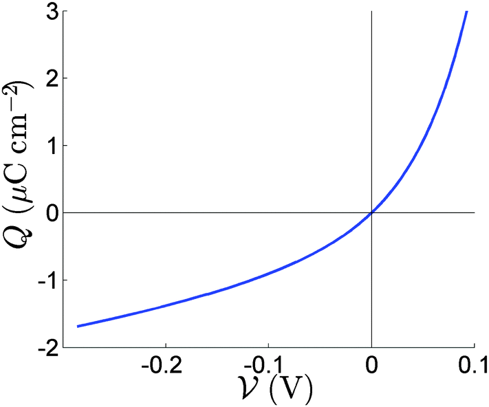 | ||
| Fig. 2 The relation between the charge Q in the Debye layer and the potential drop V across the layer. | ||
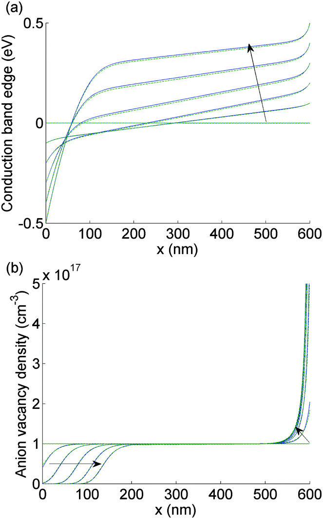 | ||
| Fig. 3 Comparison between the numerical (solid blue) and the asymptotic (dashed green) solutions to EC(x) (panel a) and P(x) (panel b) as the applied voltage V(t) is scanned from 1 V to 0 V taking values in V of 0.8, 0.6, 0.4, 0.2, 0. At time t = 0, EC(x) = 0 for all x. The arrow indicates the direction of increasing time. For this figure and Fig. 4, N0 = 1017 cm−3. | ||
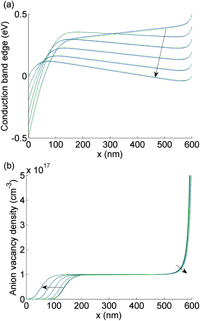 | ||
| Fig. 4 As for Fig. 3 but here V(t) is scanned from 0 V to 1 V and plotted at values in V 0, 0.2, 0.4, 0.6, 0.8, 1.0. | ||
In practice it is easier to solve directly for surface charge densities stored in the left- and right-hand Debye layers (Q− and Q+, respectively) rather than for the potential drops across these layers, V− and V+ (illustrated in Fig. 1). In order to do this it is necessary to invert the capacitance relation (1) to obtain expressions for V− and V+ in terms of Q− and Q+ of the form
| V− = V(Q−), V+ = V (Q+) where V(·) = Q−1(·). | (2) |
 | (3) |
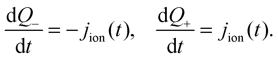 | (4) |
| Q− = −Q+. | (5) |
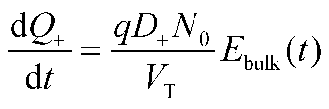 | (6) |
The equations for the drift diffusion model are well known and so are provided in ESI,† note 2 rather than the main paper. Eqn (1) and (2) of ESI,† note 2 are the continuity equations for electrons and holes combined with the equations for the current densities in terms of their diffusion and drift components. The generation rate used in this DD model is the Beer–Lambert law while charge recombination is assumed to be predominantly trap assisted and to obey Shockley–Read–Hall theory. Its numerical solution is determined by using the package Chebfun43 and yields electron and hole current densities (jn and jp, respectively) which are used to obtain an expression for the total current density across the cell J(t). Plots of J(t) versus the applied voltage V(t) yield the predicted hysteresis curves which are compared to measurements from 2 cells. The latter are made using the same process which is described in the Cell fabrication and characterization section below.
Since device history affects the measured J–V curves it is important to capture its effects accurately. After light soaking at open circuit, both cells were preconditioned at 1.2 V for 5 s, then swept from 1.2 V to 0 V and back again three times (these measurements are described below and the full results shown in ESI,† Fig. S1). The scan rate, vscan, was assigned values 1 V s−1, 500 mV s−1, 250 mV s−1 and 100 mV s−1. Further J–V curves, reported in ESI,† Fig. S2(b), were measured from cell 2, which was subsequently preconditioned for 5 s at 0 V immediately after the initial set of measurements were performed.
Two different protocols were used to model: (I) the J–V curve obtained from the third scan after the effects of the preconditioning have worn off and (II) the J–V curve obtained from the first scan immediately after the preconditioning step. Since simulating all three scans is computationally intensive we choose in case (I) to start the simulation by letting the cell equilibrate at V = 1 V (i.e. Vbi) so that the Debye layers are initially uncharged (i.e. the sweep begins at t = 0 with Q+ = 0) and then scan the voltage down from 1 V to 0 V by setting V(t) = 1 V−vscant between t = 0 to t = (1 V)/vscan and then scan back again at the same rate. Although this procedure may appear adhoc we can justify it by noting that after two cycles the preconditioning effects have worn off so that the Debye layers will be close to being uncharged (Q+ = Q− ≈ 0) at V = Vbi. In case (II) the pre-conditioning step is explicitly accounted for by starting the simulation at t = −5 s with Q+ = 0 and then immediately increasing V to 1.2 V where it remains for 5 s until t = 0, after which the downward scan is commenced with V(t) = 1.2 V − vscant from t = 0 to t = (1.2 V)/vscan; when V reaches 0 at t = (1.2 V)/vscan the direction of the scan is reversed by choosing V(t) = vscant −1.2 V between t = (1.2 V)/vscan and t = (2.4 V)/vscan. ESI,† Fig. S2(a), (c) and (d) shows predictions from our model where we follow a similar procedure to case (II), but here the preconditioning is at 0 V for 5 s before scanning to 1.2 V and back.
Cell fabrication and characterization
Methylammonium iodide was synthesized by drop-wise addition of 10 mL of HI (57 wt% in water, Sigma-Aldrich) to a cooled solution of 24 mL methylamine (33 wt% in EtOH, Sigma-Aldrich) in 100 mL ethanol under steady stirring. The solvent was removed in a rotary evaporator and then the salt was recrystallized from ethanol. Upon slowly cooling the ethanol solution, white crystals formed. Washing with diethylether and drying at 70 °C for 6 hours gave a pure product. For the compact layer of TiO2 a solution with 35 μL of 2 M HCl in 2.5 mL IPA was drop-wise added to a solution with 369 μL titanium isopropoxide (97%, Sigma-Aldrich) in 2.5 mL of IPA under heavy stirring. The solution for the hole transporting layer was mixed by dissolving 72.3 mg of spiro-MeOTAD (99%, Borun chemicals) in 1 mL chlorobenzene at ∼60 °C for 30 min and then adding 8.75μL 4-tert-butyl pyridine (tBP) and 18.75 μL Li-TFSI solution (170 mg mL−1 in acetonitrile).For device fabrication, substrates of FTO/glass (TEC7, 7 μ cm−2, Pilkington) were partially etched with Zn and 2 M HCl and cut into device sizes. Cleaning was done with Hellmanex solution (2 wt% in water), deionized water, acetone and oxygen plasma treatment for 30 min. A compact layer of TiO2 was spin-coated from the TTIP solution for 60 s at 2000 rpm (2000 rpm s−1 ramp rate) then annealed at 500 °C for 30 min.
The perovskite layer was deposited via vapour assisted solution processing, VASP.44 First, a hot solution of PbI2 (99%, Sigma-Aldrich) in DMSO (1 M, 70 °C) was spin-coated onto the heated FTO/glass substrate (70 °C) for 60 s at 2000 rpm. The PbI2 film was then annealed at 100 °C for 10 min. Conversion into perovskite films was done by vapor deposition of MAI. Therefore the MAI powder was put onto a hotplate together with the substrates and sealed with a desiccator lid. A temperature of 120 °C and low-vacuum were applied. Sublimation of the MAI converted the PbI2 into MAPbI3 within 30 min. The perovskite films were rinsed with IPA and blow-dried with nitrogen. For the hole-transporting layer the spiro solution was spread on the sample and left for 10 s before spin-coating at 4000 rpm for 45 s. Finally, a gold cathode was deposited via thermal evaporation with a shadow mask, resulting in a active area of 0.1 cm2.
A TS Space Systems solar simulator was used with a 200 W metal halide lamp and an internal AM1.5 filter, which is calibrated against a Fraunhofer reference cell (ISE, RS-OD-4). The solar simulator is classified according IEC 60904-9 Edition2 and ASTM E927-10 standards as class A. Keithley 2600A SourceMeter was used for the J–V measurements.
Two cells were prepared using the above methods, each containing ten pixels. Both cells were measured with the following protocol. The cells were connected to the solar simulator and held at open circuit, Voc, in the dark for several minutes. Then the cells were then held at Voc for 30 s under illumination to allow a steady photovoltage to be achieved. In a preconditioning stage, the cells were held at 1.2 V for 5 s. Following this stage, the cells were swept from 1.2 V to 0 V and back to 1.2 V three times. The scan rate was then reduced and the scans repeated. In ESI,† Fig. S2(b), cell 2 J–V characteristics were measured in the same way except that the preconditioning voltage was 0 V. These cell 2 measurements followed immediately after the measurements for preconditioning at 1.2 V.
3 Results
The evolution of Ebulk is illustrated in Fig. 3(a) and 4(a) and the I− vacancy concentration profile P(x,t) in Fig. 3(b) and 4(b). These figures show a series of snapshots of the solution at evenly spaced time intervals in the scans down from V = 1 V to V = 0 V and back from V = 0 V to V = 1 V, respectively. Comparison between the uniformly valid asymptotic solution and the numerical solution to the ion transport problem (green dashed and blue solid curves, respectively) is made in these figures (the agreement is extremely good).The bulk electric field Ebulk(t) is equal to the gradient of EC(x,t)/q within the central portion of the perovskite layer and is positive as V(t) is decreased from 1 V to 0 V (Fig. 3(a)), driving holes to the spiro layer and electrons to the TiO2 layer. Sharp changes in EC(x) (of magnitude qV−, qV+) are seen across the left-hand and right-hand Debye layers, respectively. Positively charged I− vacancies flow into the right-hand Debye layer, increasing Q+, and away from the left-hand Debye layer. The latter layer acquires its negative charge through vacancy depletion. Its width L− is determined by the need to maintain charge neutrality, so that
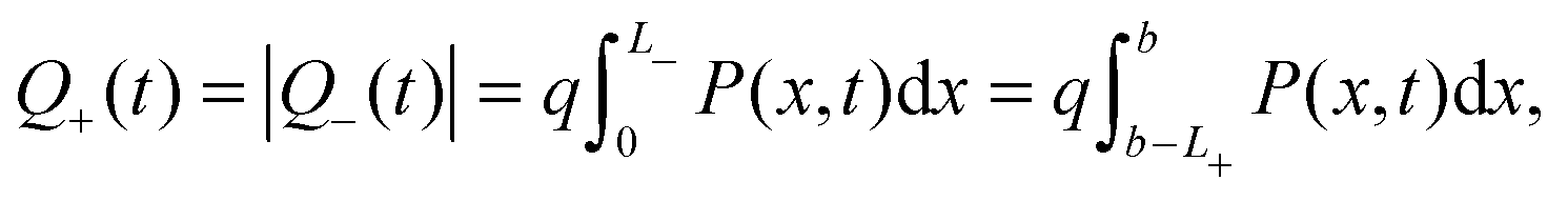 | (7) |
Note that Ebulk(t) becomes negative as V(t) returns from 0 V to 1 V (Fig. 4(a)). This change in the sign of Ebulk can be used, in part, to explain the difference between the measured current in the 1.2 V to 0 V scan from that in the 0 V to 1.2 V scan. When Ebulk < 0, the field drives the free charge carriers away from the contacts where they are extracted, into the bulk of the device, leading to large carrier concentrations and increased recombination. The charge density accumulations from the mobile vacancies Q− and Q+ influence the free charge carrier densities at the boundaries, causing diffusion currents towards or away from the contacts. These diffusion currents can exceed the drift component. In spite of this diffusion contribution, the current is typically smaller on the 0 V to 1.2 V scan than it is on the 1.2 V to 0 V scan.
Experimental J–V data from 3 complete scan cycles of cell 1 which has been preconditioned for 5 s at 1.2 V are shown in ESI,† Fig. S1(a)–(c). Fig. 5(b) plots experimental J–V data from the third scan cycle performed on cell 1. The agreement between these results and the model solutions, computed as described above, case (I) in the Methods section, and plotted in Fig. 5(a), is very good.
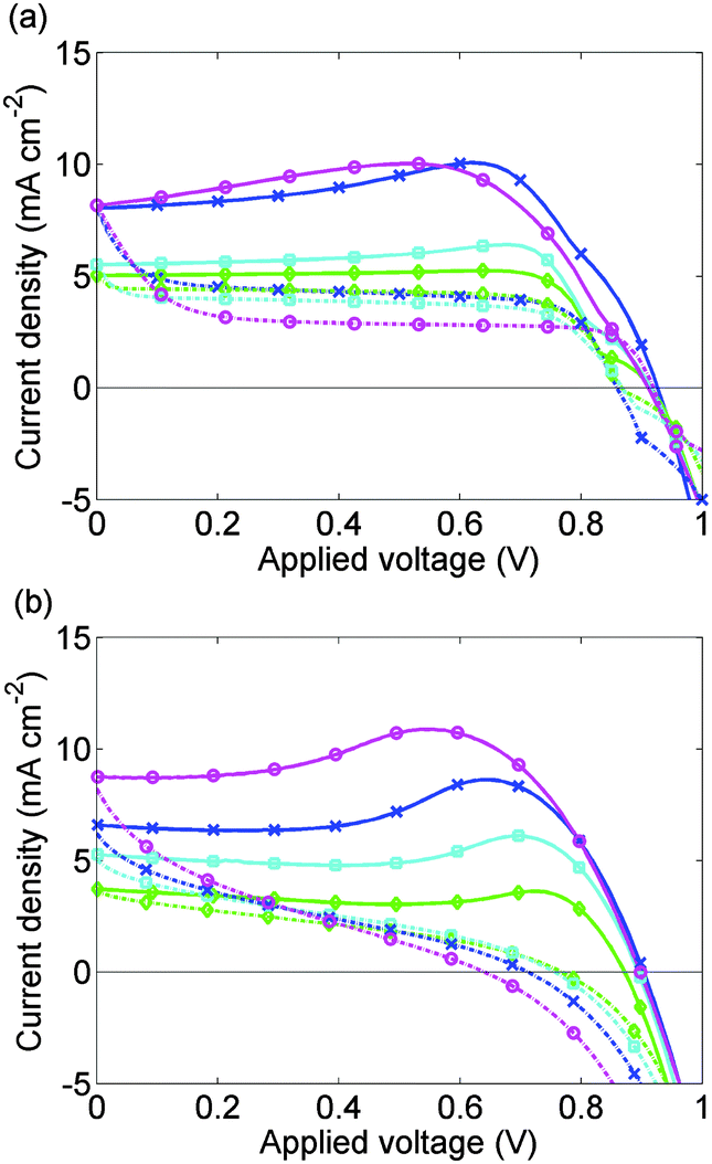 | ||
| Fig. 5 (a) Calculated J–V curves for cell 1 without allowing for preconditioning; (b) measured J–V curves for cell 1 after an initial preconditioning at 1.2 V and two scan cycles. Solid lines show the 1.2 V to 0 V scan; broken lines show the 0 V to 1.2 V scan. Scan rates are 1 V s−1 (magenta, circles), 500 mV s−1 (blue, crosses), 250 mV s−1 (cyan, filled squares), 100 mV s−1 (green, diamonds). As discussed in the text the third scans are shown as the effect of the 1.2 V preconditioning is removed. | ||
Fig. 6 depicts the evolution of the bulk electric field Ebulk and the Debye layer surface charge density Q+ arising from the vacancy motion predicted by the model used to simulate the J–V curves in Fig. 5(a). As noted previously where Ebulk(t) > 0, positively charged I− vacancies flow into the right-hand Debye layer, increasing Q+. For large positive Q+, the potential drop across the left-hand Debye layer, −V−, is large and positive and screens out the field from the potential across the contacts. In the subsequent 0 V to 1 V scan the screening, which lags behind the scan, typically leads to negative Ebulk, putting the cell into effective forward bias and leading to high recombination rates.
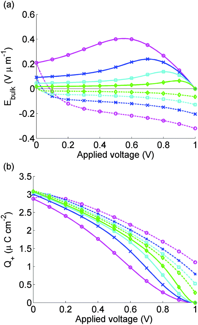 | ||
| Fig. 6 Electric field between the Debye layers Ebulk (panel a) and charge per unit area in the Debye layer next to the spiro Q+ (panel b) used to find calculated J–V curves for cell 1 shown in Fig. 5. Scan rates and solid and dashed lines as for Fig. 5. | ||
The model is able to predict the maximum in the current density on the 1 V to 0 V scan, seen in measurements reported here and elsewhere.9,11 This is closely associated with a maximum in Ebulk the field that drives the charge carriers apart. This result strengthens the hypothesis that large positive values of Ebulk suppress recombination, increasing current output.
The vacancy mediated ion motion hypothesis provides a clear explanation for the influence of scan rate on J–V curves. For slower scan rates, the vacancies have more time to respond to the change in applied voltage than for faster scans. Hence, the vacancy charge screens the bulk electric field more effectively on slower scans than on fast ones, so |Ebulk| remains relatively small on such slow scans, resulting in limited hysteresis. For intermediate scan rates, hysteresis is strongest. At the other extreme, if the scan is sufficiently fast, the ions do not have a chance to build up in the Debye layers so that there is very limited screening and consequently little hysteresis (and increased short circuit current). This effect is not addressed here but is reported elsewhere.10,11
Snaith et al.8 also report an increase in hysteresis with reduction in scan rate even at scan rates as low as 11 mV s−1. This observation contrasts with our data which suggests that hysteresis is reduced by a decrease in scan rates below about 1 V s−1. The 1.4 V to 0 V scans in ref.8 vary little with scan rate, which could be a result of the strong preconditioning (60 s at 1.4 V) used. It may be the case that this strong preconditioning makes Ebulk high enough to yield a large current for the whole of 1.4 V to 0 V and 0 V to 1.4 V scans, unless the scan rate is very slow. Only when Snaith et al.8 decreased the scan rate to 11 mV s−1 did the current maximum reappear.
Deviations between the experimental and theoretical results occur for the fastest scan rate, 1 V s−1, and when the applied voltage is increasing from 0 V to 1 V. For the calculated 0 V to 1 V scans, J is nearly independent of V except for sharp changes in J close to open circuit. In contrast, the measured 0 V to 1.2 V scans have a continuously varying slope. Evidence from an analytic solution to the DD carrier equations that we have derived when τp = 0 suggests that decreasing τp towards zero could help correct this discrepancy between experiment and theory. However for τp < τn/100, the DD equations for the free charge carriers become so stiff that numerical solutions become very difficult to find.
Experimental J–V data from 3 complete scan cycles of cell 2, which like cell 1 has been preconditioned for 5 s at 1.2 V, are shown in ESI,† Fig. S1(d)–(f). These plots show how the effects of the preconditioning step diminish over successive scan cycles. In Fig. 7(b), this data is shown for the first scan cycle. Preconditioning plays a significant role in the subsequent evolution of the J–V curve in contrast to the data presented in Fig. 5(b) for the third scan cycle.
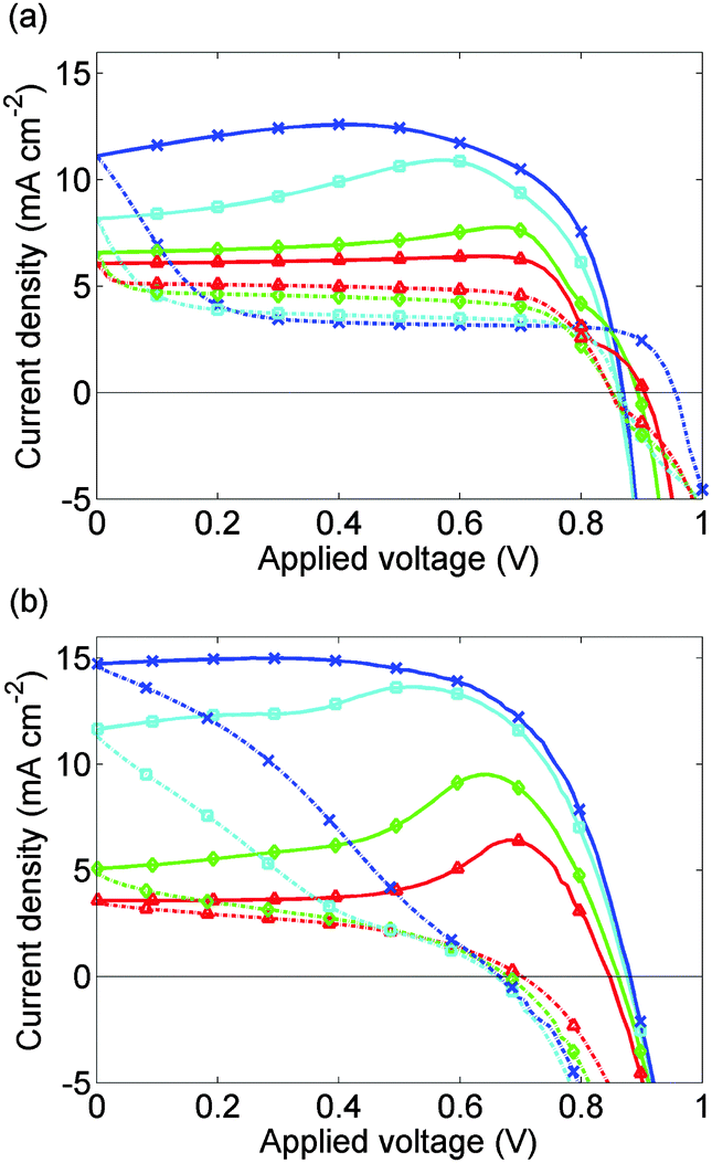 | ||
| Fig. 7 (a) Calculated J–V curves for cell 2 allowing for 5 s preconditioning at 1.2 V. (b) Measured J–V curves for cell 2 on the 1st scan cycle immediately after preconditioning for 5 s at 1.2 V. Solid lines show the 1.2 V to 0 V scan; broken lines show the 0 V to 1.2 V scan. Scan rates are as for Fig. 5 with the addition of a scan rate of 50 mV s−1 (red, triangles). In the fastest scans the shapes of the J–V curves are improved by the preconditioning. | ||
The simulated J–V curve for cell 2, computed using case (II) in the Methods section, is plotted in Fig. 7(a) while the solution for Ebulk and Q+ are plotted in Fig. 8. Comparison to experimental data, though still good, is not as good as in Fig. 5. This discrepancy may arise because the preconditioning step occurs at 1.2 V, outside the range V ≤ 1V in which the effect of electrons and holes on the potential can be neglected. The model therefore overpredicts the charge accumulation (negative Q+) in the preconditioning step. The sensitivity to preconditioning seen in Fig. 7(a) and (b) was also observed by O'Regan et al.20
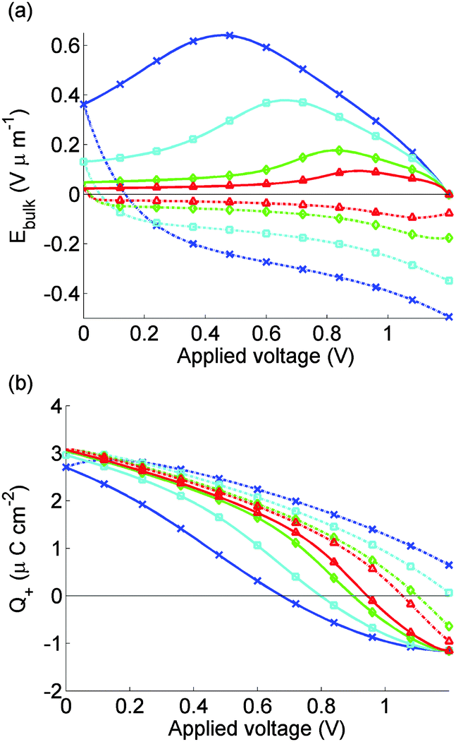 | ||
| Fig. 8 As for Fig. 6, but for calculated J–V curves for cell 2 shown in Fig. 7 where we model effects of 5 s preconditioning at FB = 1.2 V. | ||
On commencing preconditioning, Q+ = 0. Since the preconditioning occurs at 1.2 V which exceeds Vbi, the net field in the bulk of the perovskite layer Ebulk is negative. As a consequence, the I− vacancies drift towards the TiO2 layer. A net negative charge is left next to the spiro layer, causing Q+ to become progressively more negative. This negative Q+ gives a negative V+ and a positive V− which is opposite to the signs depicted in Fig. 1. By the end of the relatively short preconditioning period, the net voltage drop of −0.2 V is nearly all accounted for by V+ and V− so that Ebulk ≈ 0.
Once the scan begins, V(t) begins to drop. However it takes time for the vacancies to move away from their accumulation layer and for Q+ to increase from its negative value, so the reduction in Ebulk from V+ and V− is less than it would have been without the preconditioning. This result aids extraction of electrons into the TiO2 and holes into the spiro and explains the widely reported observation that preconditioning at a voltage exceeding Vbi improves the apparent solar cell performance.
4 Conclusions
In conclusion, a time-dependent drift-diffusion model has been developed to explore the effects of defect mediated ion motion on the J–V curves of planar perovskite solar cells. We have shown that an accurate representation of the ionic charge buildup in narrow Debye layers close to the blocking layers is crucial to understanding the experimental J–V curves reported here.Our model predicts hysteresis that compares well to the experimental data reported here and which is similar to that reported in the literature. The hypothesis that mobile ions in the perovskite are responsible for hysteresis is confirmed, although other explanations, such as large-scale trapping of electrons,45 are not ruled out. We have also shown why apparently high efficiencies, obtained from measurements at fast scan rates, are not a useful indicator of device performance, even over several voltage cycles. Our approach can be generalized to explore recombination schemes other than the one considered here, to accommodate multiple ion species with different mobilities and to study why hysteresis effects increase as the temperature decreases, even in low hysteresis cells.46,47
The markedly lower hysteresis observed in perovskite solar cells employing a 60-PCBM hole blocking layer has been attributed by Shao et al.35 to passivation of perovskite grain boundaries by the PCBM. This explanation has been questioned by Tao et al.48 who note that the PCBM layer is so thin (∼40 nm) in comparison to the perovskite layer (b ≈ 300–600 nm) that the amount of PCBM leakage required for effective passivation is enough to cause degradation of the PCBM layer and reduce device performance. The moving ion hypothesis, however, points to an alternative explanation for the lower hysteresis in these cells. Under normal operating conditions (i.e. V < Vbi), vacancies drift towards the spiro (PEDOT:PSS for inverted structures) and away from the PCBM, i.e. I− ions move towards the PCBM. Since PCBM is made up of small molecules of functionalized C60 it is quite possible that I− ions could drift across the interface entering gaps between the PCBM molecules. This cannot happen in titania, which is crystalline. It is also possible that positively charged ions, e.g. Li+ from the spiro, protons or MA+, could enter the PCBM, compensating the negative charge of the iodide ions and causing the hysteretic effect to be further reduced.
Acknowledgements
The authors wish to acknowledge helpful discussions with Laurie Peter, Saiful Islam and Aron Walsh. The research leading to these results has received funding from the European Union Seventh Framework Programme FP7/2007-2013 under grant agreement 316494 and the UK Engineering and Physical Sciences Research Council grants EP/J017361/1 & EP/I01702X/1.References
- A. Kojima, K. Teshima, Y. Shirai and T. Miyasaka, J. Am. Chem. Soc., 2009, 131, 6050–6051 CrossRef CAS PubMed.
- M. M. Lee, J. Teuscher, T. Miyasaka, T. N. Murakami and H. J. Snaith, Science, 2012, 338, 643–647 CrossRef CAS PubMed.
- H.-S. Kim, C.-R. Lee, J.-H. Im, K.-B. Lee, T. Moehl, A. Marchioro, S.-J. Moon, R. Humphry-Baker, J.-H. Yum, J. E. Moser, M. Graetzel and N.-G. Park, Sci. Rep., 2012, 2, 591 Search PubMed.
- S. D. Stranks and H. J. Snaith, Nat. Nanotechnol., 2015, 10, 391–402 CrossRef CAS PubMed.
- G. Niu, X. Guo and L. Wang, J. Mater. Chem. A, 2015, 3, 8970–8980 CAS.
- T. Miyasaka, Chem. Lett., 2015, 44, 720 CrossRef CAS.
- N.-G. Park, J. Phys. Chem. Lett., 2013, 4, 2423–2429 CrossRef CAS.
- H. J. Snaith, A. Abate, J. M. Ball, G. E. Eperon, T. Leijtens, N. K. Noel, S. D. Stranks, J. T.-W. Wang, K. Wojciechowski and W. Zhang, J. Phys. Chem. Lett., 2014, 5, 1511–1515 CrossRef CAS PubMed.
- R. S. Sanchez, V. Gonzalez-Pedro, J.-W. Lee, N.-G. Park, Y. S. Kang, I. Mora-Sero and J. Bisquert, J. Phys. Chem. Lett., 2014, 5, 2357–2363 CrossRef CAS PubMed.
- E. L. Unger, E. T. Hoke, C. D. Bailie, W. H. Nguyen, A. R. Bowring, T. Heumuller, M. G. Christoforo and M. D. McGehee, Energy Environ. Sci., 2014, 7, 3690–3698 CAS.
- W. Tress, N. Marinova, T. Moehl, S. M. Zakeeruddin, M. K. Nazeeruddin and M. Grätzel, Energy Environ. Sci., 2015, 8, 995–1004 CAS.
- T. C. Sum, S. Chen, G. Xing, X. Liu and B. Wu, Nanotechnology, 2015, 26, 342001 CrossRef PubMed.
- J. Gong, S. B. Darling and F. You, Energy Environ. Sci., 2015, 8, 1953–1968 CAS.
- J. Berry, T. Buonassisi, D. A. Egger, G. Hodes, L. Kronik, Y.-L. Loo, I. Lubomirsky, S. R. Marder, Y. Mastai, J. S. Miller, D. B. Mitzi, Y. Paz, A. M. Rappe, I. Riess, B. Rybtchinski, O. Stafsudd, V. Stevanovic, M. F. Toney, D. Zitoun, A. Kahn, D. Ginley and D. Cahen, Adv. Mater., 2015, 35, 5102 CrossRef PubMed.
- X. Li, X. Wang, W. Zhang, Y. Wu, F. Gao and J. Fang, Org. Electron., 2015, 18, 107–112 CrossRef CAS.
- J. M. Frost, K. T. Butler, F. Brivio, C. H. Hendon, M. van Schilfgaarde and A. Walsh, Nano Lett., 2014, 14, 2584–2590 CrossRef CAS PubMed.
- J. Beilsten-Edmands, G. E. Eperon, R. D. Johnson, H. J. Snaith and P. G. Radaelli, Appl. Phys. Lett., 2015, 106, 173502 CrossRef.
- H.-S. Kim, I.-H. Jang, N. Ahn, M. Choi, A. Guerrero, J. Bisquert and N.-G. Park, J. Phys. Chem. Lett., 2015, 6, 4633–4639 CrossRef CAS PubMed.
- Y. Zhang, M. Liu, G. E. Eperon, T. C. Leijtens, D. McMeekin, M. Saliba, W. Zhang, M. de Bastiani, A. Petrozza, L. M. Herz, M. B. Johnston, H. Lin and H. J. Snaith, Mater. Horiz., 2015, 2, 315–322 RSC.
- B. C. O'Regan, P. R. F. Barnes, X. Li, C. Law, E. Palomares and J. M. Marin-Beloqui, J. Am. Chem. Soc., 2015, 137, 5087–5099 CrossRef PubMed.
- T.-Y. Yang, G. Gregori, N. Pellet, M. Grätzel and J. Maier, Angew. Chem., Int. Ed., 2015, 54, 7905 CrossRef CAS PubMed.
- C. Eames, J. M. Frost, P. R. F. Barnes, B. C. O'Regan, A. Walsh and M. S. Islam, Nat. Commun., 2015, 6, 7497 CrossRef CAS PubMed.
- J. M. Azpiroz, E. Mosconi, J. Bisquert and F. De Angelis, Energy Environ. Sci., 2015, 8, 2118–2127 CAS.
- A. Walsh, J. Phys. Chem. C, 2015, 119, 5755–5760 CAS.
- J. Nelson, The physics of solar cells, Imperial College Press, London, UK, 2003 Search PubMed.
- J. M. Foster, H. J. Snaith, T. Leijtens and G. Richardson, SIAM J. Appl. Math., 2014, 74, 1935–1966 CrossRef.
- S. Guarnera, A. Abate, W. Zhang, J. M. Foster, G. Richardson, A. Petrozza and H. J. Snaith, J. Phys. Chem. Lett., 2015, 6, 432–437 CrossRef CAS PubMed.
- J. O. Bokris, A. K. Reddy and M. E. Gamboa-Aldeco, Modern Electrochemistry 2A, Springer US, New York, 2000 Search PubMed.
- R. Morrow and D. R. McKenzie, Proc. R. Soc. A, 2011, 468, 18–34 CrossRef.
- A. Walsh, D. O. Scanlon, S. Chen, X. G. Gong and S.-H. Wei, Angew. Chem., 2015, 127, 1811 CrossRef.
- T. Minemoto and M. Murata, J. Appl. Phys., 2014, 116, 054505 CrossRef.
- F. Liu, J. Zhu, J. Wei, Y. Li, M. Lv, S. Yang, B. Zhang, J. Yao and S. Dai, Appl. Phys. Lett., 2014, 104, 253508 CrossRef.
- X. He, K. Juan Jin, C. Ge, C. Wang, H. Bin Lu and G. Zhen Yang, EPL, 2013, 102, 37007 CrossRef.
- S. van Reenen, M. Kemerink and H. J. Snaith, J. Phys. Chem. Lett., 2015, 6, 3808–3814 CrossRef CAS PubMed.
- Y. Shao, Z. Xiao, C. Bi, Y. Yuan and J. Huang, Nat. Commun, 2014, 5, 5784 CrossRef CAS PubMed.
- E. T. Hoke, D. J. Slotcavage, E. R. Dohner, A. R. Bowring, H. I. Karunadasa and M. D. McGehee, Chem. Sci., 2015, 6, 613–617 RSC.
- P. Schulz, E. Edri, S. Kirmayer, G. Hodes, D. Cahen and A. Kahn, Energy Environ. Sci., 2014, 7, 1377–1381 CAS.
- F. Brivio, K. T. Butler, A. Walsh and M. van Schilfgaarde, Phys. Rev. B: Condens. Matter Mater. Phys., 2014, 89, 155204 CrossRef.
- A. Pockett, G. E. Eperon, T. Peltola, H. J. Snaith, A. Walker, L. M. Peter and P. J. Cameron, J. Phys. Chem. C, 2015, 119, 3456–3465 CAS.
- S. Sun, T. Salim, N. Mathews, M. Duchamp, C. Boothroyd, G. Xing, T. C. Sum and Y. M. Lam, Energy Environ. Sci., 2014, 7, 399–407 CAS.
- Y. Kato, L. K. Ono, M. V. Lee, S. Wang, S. R. Raga and Y. Qi, Adv. Mater. Interfaces, 2015, 2, 1500195 Search PubMed.
- G. Richardson, Mathematical Medicine and Biology, 2009, 26, 201–224 CrossRef CAS PubMed.
- T. A. Driscoll, N. Hale and L. N. Trefethen, Chebfun Guide, Panufty Publications, Oxford, 2014 Search PubMed.
- Q. Chen, H. Zhou, Z. Hong, S. Luo, H.-S. Duan, H.-H. Wang, Y. Liu, G. Li and Y. Yang, J. Am. Chem. Soc., 2014, 136, 622–625 CrossRef CAS PubMed.
- J. H. Heo, D. H. Song, H. J. Han, S. Y. Kim, J. H. Kim, D. Kim, H. W. Shin, T. K. Ahn, C. Wolf, T.-W. Lee and S. H. Im, Adv. Mater., 2015, 27, 3424–3430 CrossRef CAS PubMed.
- D. Bryant, S. Wheeler, B. C. O'Regan, T. Watson, P. R. F. Barnes, D. Worsley and J. Durrant, J. Phys. Chem. Lett., 2015, 6, 3190–3194 CrossRef CAS.
- L. K. Ono, S. R. Raga, S. Wang, Y. Kato and Y. Qi, J. Mater. Chem. A, 2015, 3, 9074–9080 CAS.
- C. Tao, S. Neutzner, L. Colella, S. Marras, A. R. Srimath Kandada, M. Gandini, M. D. Bastiani, G. Pace, L. Manna, M. Caironi, C. Bertarelli and A. Petrozza, Energy Environ. Sci., 2015, 8, 2365–2370 CAS.
Footnote |
| † Electronic supplementary information (ESI) available. See DOI: 10.1039/c5ee02740c |
| This journal is © The Royal Society of Chemistry 2016 |