
 Open Access Article
 This Open Access Article is licensed under a Creative Commons Attribution-Non Commercial 3.0 Unported Licence
Charge carrier dynamics of methylammonium lead iodide: from PbI2-rich to low-dimensional broadly emitting perovskites†
Johannes R.
Klein
,
Oliver
Flender
,
Mirko
Scholz
,
Kawon
Oum
* and
Thomas
Lenzer
*
Universität Siegen, Physikalische Chemie, Adolf-Reichwein-Str. 2, 57076 Siegen, Germany. E-mail: oum@chemie.uni-siegen.de; lenzer@chemie.uni-siegen.de
First published on 14th March 2016
Abstract
We provide an investigation of the charge carrier dynamics of the (MAI)x(PbI2)1−x system in the range x = 0.32–0.90 following the recently published “pseudobinary phase-composition processing diagram” of Song et al. (Chem. Mater., 2015, 27, 4612). The dynamics were studied using ultrafast pump-supercontinuum probe spectroscopy over the pump fluence range 2–50 μJ cm−2, allowing for a wide variation of the initial carrier density. At high MAI excess (x = 0.90), low-dimensional perovskites (LDPs) are formed, and their luminescence spectra are significantly blue-shifted by ca. 50 nm and broadened compared to the 3D perovskite. The shift is due to quantum confinement effects, and the inhomogeneous broadening arises from different low-dimensional structures (predominantly 2D, but presumably also 1D and 0D). Accurate transient carrier temperatures are extracted from the transient absorption spectra. The regimes of carrier–carrier, carrier–optical phonon and acoustic phonon scattering are clearly distinguished. Perovskites with mole fractions x ≤ 0.71 exhibit extremely fast carrier cooling (ca. 300 fs) at low fluence of 2 μJ cm−2, however cooling slows down significantly at high fluence of 50 μJ cm−2 due to the “hot phonon effect” (ca. 2.8 ps). A kinetic analysis of the electron–hole recombination dynamics provides second-order recombination rate constants k2 which decrease from 5.3 to 1.5 × 10⁻⁹ cm3 s−1 in the range x = 0.32–0.71. In contrast, recombination in the LDPs (x = 0.90) is more than one order of magnitude faster, 6.4 × 10⁻⁸ cm3 s−1, which is related to the confined perovskite structure. Recombination in these LDPs should be however still slow enough for their potential application as efficient broadband emitters or solar light-harvesting materials.
1. Introduction
Methylammonium lead iodide (MAPbI3) and related organic–inorganic hybrid perovskites hold great promise as efficient future materials for solar energy conversion.1–5 They are fully solution-processible at moderate synthetic effort and still retain very good electronic properties. This makes them an excellent alternative not only for photovoltaic devices, but possibly also for (opto)electronic applications, such as photodiodes, LEDs or transistors.6,7Different design principles have been devised for perovskite solar cell devices, employing mainly three-dimensional arrangements deposited on mesoporous TiO2 scaffolds or integrated in thin film architectures without a mesoporous oxide layer.2,8 In addition, layered hybrid perovskite solar-cell absorbers have been synthesized where the perovskite is deposited as a low-dimensional perovskite phase.9–14 This approach might offer advantages regarding tunability of the band-gap, broadband emission properties and stability of the perovskite against humidity.10,11
Previously, we presented a comprehensive UV-Vis broadband transient absorption study (320–920 nm) of the ultrafast carrier dynamics of MAPbI3 on TiO2 prepared via different synthetic routes.15 The perovskite was deposited using 1-step or 2-step deposition methods. In the latter case, first a PbI2 solution was spin-coated onto a mesoporous TiO2 scaffold with subsequent spin-coating of a methylammonium iodide (MAI) solution which generated the desired perovskite in an on-surface reaction based on modified literature procedures.16–19 The relaxation dynamics of the charge carriers in MAPbI3 were completely resolved up to 700 ps.15 A sub-bandgap transient absorption feature caused by hot carriers was clearly identified at early times and related to band-gap renormalization. In addition, accurate carrier temperatures were extracted from Boltzmann fits to the high-energy tail of the carrier distribution, yielding characteristic transient carrier temperature cooling curves T(t) for two different initial carrier excitation energies. These enabled us to identify the partially overlapping time scales of different carrier cooling regimes, such as carrier–carrier and carrier–optical phonon scattering and acoustic phonon relaxation.15 Carrier cooling curves and the sub-bandgap hot-carrier absorption feature due to band-gap renormalization were confirmed in a later study by Price et al.20
In the current work, we control the composition of the (MAI)x(PbI2)1−x system via the initial MAI and PbI2 mole fractions used in a 1-step deposition process, and study its impact on the steady-state absorption and luminescence spectra as well as the ultrafast carrier dynamics of the resulting material. Beside the equimolar regime, which was in the focus of our previous study,15 the present work includes PbI2-rich phases for low MAI concentrations as well as stacked perovskite sheets and low-dimensional perovskite phases at high MAI content over the mole fraction range x = 0.32–0.90. We will correlate our data with the results of a previous thorough study of Song et al. who proposed a “pseudobinary phase-composition processing diagram” for the (MAI)x(PbI2)1−x system.12 As an extension of our earlier work,15 we also investigate the carrier dynamics for all of these systems over a broad range of carrier densities, down to the low fluence limit.
2. Experimental
Thoroughly cleaned and dried microscope glass slides of 1 mm thickness were employed as substrates for preparing perovskite/TiO2 layers. The TiO2 thin films were prepared from a 1![[thin space (1/6-em)]](https://www.rsc.org/images/entities/char_2009.gif) :9 mixture (by volume) of TiO2 paste (Dyesol DSL 90T) and 2-propanol (Fisher Scientific, p.a., 99.97%). The mixture was sonicated for 20 minutes. After doctor blading and subsequent sintering at 450 °C, mesoporous TiO2 films of high transparency were obtained (thickness ca. 300 nm).
:9 mixture (by volume) of TiO2 paste (Dyesol DSL 90T) and 2-propanol (Fisher Scientific, p.a., 99.97%). The mixture was sonicated for 20 minutes. After doctor blading and subsequent sintering at 450 °C, mesoporous TiO2 films of high transparency were obtained (thickness ca. 300 nm).
The perovskite synthesis was carried out in a N2-filled glove-box at a controlled humidity of <2%. In order to ensure an accurate stoichiometry of the final material, a modified 1-step method based on the recipes of Heo and co-workers and Im et al. was employed:16,17 PbI2 (Sigma Aldrich, 99%) and MAI (Dyenamo) were dissolved in dimethylformamide (DMF, Fisher Scientific, p.a., 99.99%) and stirred for 30 min at 25 °C. The solution was spin-coated at 25 °C for 4 s at 500 rpm (without initial loading time) and then 30 s at 2000 rpm. For the experiments employing different MAI mole fractions x = n(MAI)/[n(MAI) + n(PbI2)], the films were annealed for 60 min at 90 °C on a hotplate. In addition, systematic studies using different heating times (15, 30 and 60 min) and a higher temperature of 107 °C were carried out.
The characterization of the thin films was performed by X-ray diffraction (XRD) at T = 294 K using a PANalytical X’Pert MPD PRO diffractometer, as described previously.15 Steady-state absorption spectra over the spectral range 200–2000 nm were measured using a Varian Cary 5000 spectrophotometer, and photoluminescence spectra were recorded on an Agilent Cary Eclipse spectrometer. All steady-state photoluminescence and UV-Vis absorption experiments were performed at T = 296 K under N2 atmosphere.
Ultrafast Vis-NIR transient absorption spectra in the wavelength range 500–920 nm were recorded using pump-supercontinuum probe (PSCP) spectroscopy at T = 296 K.21–26 Samples were mounted inside a home-built aluminum gas flow cell with a Suprasil I substrate as back window and constantly purged by gaseous nitrogen (purity 4.6). The cell was permanently translated during the course of the experiments by a fast piezo x/y translation stage, so that each laser shot was hitting a fresh sample spot. A NOPA was used for sample excitation (λpump = 500 nm), with the pump beam entering the TiO2/perovskite layer through the microscope glass slide. Pump fluences of 2, 14 and 50 μJ cm−2 were adjusted by means of pellicle beam splitters, leading to average values of ca. 4.6 × 10¹², 3.2 × 10¹³ and 1.2 × 10¹⁴ photons cm−2, respectively. The pump beam diameter at the sample was controlled using a calibrated CCD camera, and the pulse energy was measured by a calibrated photodiode detector. The relative pump/probe polarization was set at magic angle (54.7°). Chirp-correction was performed using the coherent response of a TiO2/glass sample. The pump–probe intensity cross-correlation time was ca. 80 fs, with a time zero accuracy of ca. 10 fs.
3. Results and discussion
3.1 X-ray diffractions patterns
XRD patterns of (MAI)x(PbI2)1−x prepared using different mole fractions of MAI are shown in Fig. 1. We commence with x = 0.51 (green line) for the approximately equimolar MAI/PbI2 mixture which represents the reference for formation of a stoichiometric perovskite. Indeed, we find characteristic diffraction peaks at 14.1, 28.4, and 31.8° for the tetragonal MAPbI3 phase.12,19 | ||
| Fig. 1 XRD patterns of (MAI)x(PbI2)1−x/TiO2/glass samples as a function of the initial mole fraction x of MAI. The materials were deposited by a single-step deposition process from DMF. Black, green, red and blue lines are the XRD patterns for x = 0.32, 0.51, 0.71 and 0.90, respectively. | ||
In the case of x = 0.32 (black line), an excess of PbI2 exists. Therefore, in addition to the characteristic XRD peaks of the perovskite, we observe clear signals at 12.7° and 39.6°, which are assigned to the hexagonal 2H polytype of PbI2.12,19 Therefore, the sample must consist of a MAPbI3/PbI2 mixture.12
Going into the MAI-rich region, the XRD pattern for x = 0.71 (red line) very much resembles that of the perovskite for x = 0.51. This finding is in agreement with the suggestion of Song et al. that 3D-type perovskite structures with limited numbers of stacking faults, so-called stacked perovskite sheets (SPS), may exist up to at least x ≈ 0.80.12 At short annealing times (15 min) we observe a peak at 11.5° which is characteristic for low-dimensional perovskite (LDP) structures, however it disappears after 60 min annealing time (see Fig. S1 in the ESI†), in agreement with the finding of Song et al.,12 indicating a rearrangement or transformation of the LDP structure.
In the case of the composition starting with even higher MAI excess (x = 0.90, blue line), the XRD pattern changes drastically. The peak centered at 2θ = 11.5° is now intense and broad suggesting the dominant formation of polydisperse LDPs featuring 2D (sheet), 1D (chain) and 0D (quantum dot) structures. These are typically separated by layer(s) of intercalated methylammonium cations.12 Other intense diffraction peaks, such as those at 9.8°, 19.7° and 29.8°, are assigned to an MAI phase.12
On the technical side, we would like to note that the optimized annealing condition for (MAI)x(PbI2)1−x synthesis was heating the thin films for 60 min at a temperature of 90 °C. During that time, the XRD spectra showed no sample deterioration, as demonstrated by the XRD data in Fig. S2 of the ESI,† and it is likely that these longer annealing times improve the crystallinity of the sample and further help to remove any residual solvent. Using a higher temperature of 107 °C leads to perovskite decomposition already after 15 min, with almost complete formation of PbI2 after 60 min (Fig. S2, ESI†).
3.2 Steady-state absorption and luminescence spectra
Steady-state Vis-NIR absorption and photoluminescence spectra for (MAI)x(PbI2)1−x, prepared using the same MAI mole fractions as above, are presented in Fig. 2. For x = 0.51 (green line), one observes the characteristic absorption spectrum of the MAPbI3 perovskite, with a red absorption edge corresponding to the band gap of 760 nm, a growing absorption toward the UV and a shoulder located near 500 nm.15 The corresponding luminescence spectrum is sharp, with a peak at 762 nm and a FWHM of 750 cm−1. The FWHM is consistent with an estimate based on a very simple line shape analysis which predicts a value of ca. 700 cm−1 for a temperature of 296 K.27 | ||
| Fig. 2 Steady-state absorption (left) and photoluminescence spectra (right) of (MAI)x(PbI2)1−x/TiO2/glass prepared using different initial mole fractions x of MAI. Black: 0.32, green: 0.51, red: 0.71, blue: 0.90. For the sake of an easier comparison, absorption spectra are set to zero at 840 nm. Photoluminescence spectra are normalized to their peak amplitude. | ||
The PbI2-rich perovskite (x = 0.32, black line) exhibits the same step at 760 nm, which is characteristic for MAPbI3, however with a roughly by a factor of three smaller amplitude. In addition, the shoulder at 500 nm is steeper and more pronounced. This is exactly the position where the band edge of PbI2 is located,15 so this is another clear indication that a PbI2 phase is present in the material. The luminescence spectrum is virtually identical to that of the perovskite for x = 0.51 (λmax = 761 nm, FWHM 760 cm−1). In separate experiments for PbI2/TiO2/glass, we observed that the luminescence of PbI2 is weak and difficult to detect. Moreover, reabsorption by the strongly absorbing perovskite will likely reduce the luminescence of PbI2 even further.
In the case of the MAI-enriched sample with x = 0.71 (red line), the absorption spectrum shows again the same position of the band edge at ca. 760 nm, this time with a slightly larger amplitude than for x = 0.51. The shoulder at 500 nm is much weaker. The shape is likely dominated by the absorption of SPS. A slight blue-shift and an increase of the width of the band of the luminescence spectrum are observed (λmax = 752 nm, FWHM 800 cm−1). This is taken as an indication that LDP structures are present, compare e.g. also Fig. S1 (ESI†).
Dramatic changes are observed for the strongly MAI-enriched sample (x = 0.90, blue line). The characteristic absorption band edge of MAPbI3 completely disappears, and instead a much wider step in the wavelength range 600–700 nm becomes apparent. The shoulder at 500 nm vanishes, and the whole spectrum monotonously rises toward the UV. The luminescence spectrum is drastically shifted to shorter wavelengths (λmax = 706 nm) and becomes extremely broad (FWHM 1490 cm−1). This width is more than twice as large than expected for a typical semiconductor material at this temperature.27 Based on the XRD data in Fig. 1, the strongly blue-shifted band edge absorption and emission band arise from different low-dimensional perovskite species (2D, 1D and even 0D). The increase in band-gap should be then due to a quantum confinement effect. This was e.g. previously observed for well-defined nanoplatelets made up of organometal bromide perovskite.28,29 The large FWHM reflects strong inhomogeneous broadening due to the superposition of emission from several species with different band gaps. In fact, such a broad emission might be advantageous for specific applications, e.g., in cases where broadly emitting LED materials are required.11
3.3 Carrier cooling dynamics for mole fractions x ≤ 0.71
Transient Vis-NIR PSCP broadband absorption spectra for the lowest and highest pump fluences of 2 μJ cm−2 and 50 μJ cm−2 are shown in Fig. 3 and 4, respectively. Another example for the intermediate pump fluence of 14 μJ cm−2 is provided in Fig. S3 (ESI†). Selected kinetic traces can be found in Fig. 5(A–C). Each column in Fig. 3 and 4 depicts the results for (MAI)x(PbI2)1−x prepared using a well-defined mole fraction x, going from a PbI2-enriched system (0.32, A) to almost pure MAPbI3 perovskite (0.51, B), SPS perovskite with small LDP contributions (0.71, C) and finally LDPs (0.90, D). The LDP case will be separately dealt with in Section 3.4. The top, middle and bottom panels illustrate the spectral behavior on different time scales. The data are also presented as contour plots in (A′–D′). | ||
| Fig. 3 Transient Vis-NIR PSCP broadband absorption spectra of (MAI)x(PbI2)1−x/TiO2/glass at a pump pulse fluence of 2 μJ cm−2 for different initial mole fractions x. Columns (A) to (D) are the results for x = 0.32, 0.51, 0.71 and 0.90, respectively. (top panels) −0.10…0.15 ps with 50 fs steps; 0.45 ps, 0.90 ps; (middle panels) 1.5, 6.0, 15 and 40 ps; (bottom panels) 100, 200, 500 and 800 ps. Selected transient spectra are shown as thick colored lines for guidance. The blue-dotted lines in the bottom panels are the scaled steady-state stimulated emission spectra. (A′–D′) Show the dynamics of the systems in (A–D) as contour plots using a logarithmic time scale. White, pink and bluish colors denote bleach or stimulated emission, whereas green, yellow and red colors correspond to transient absorption. | ||
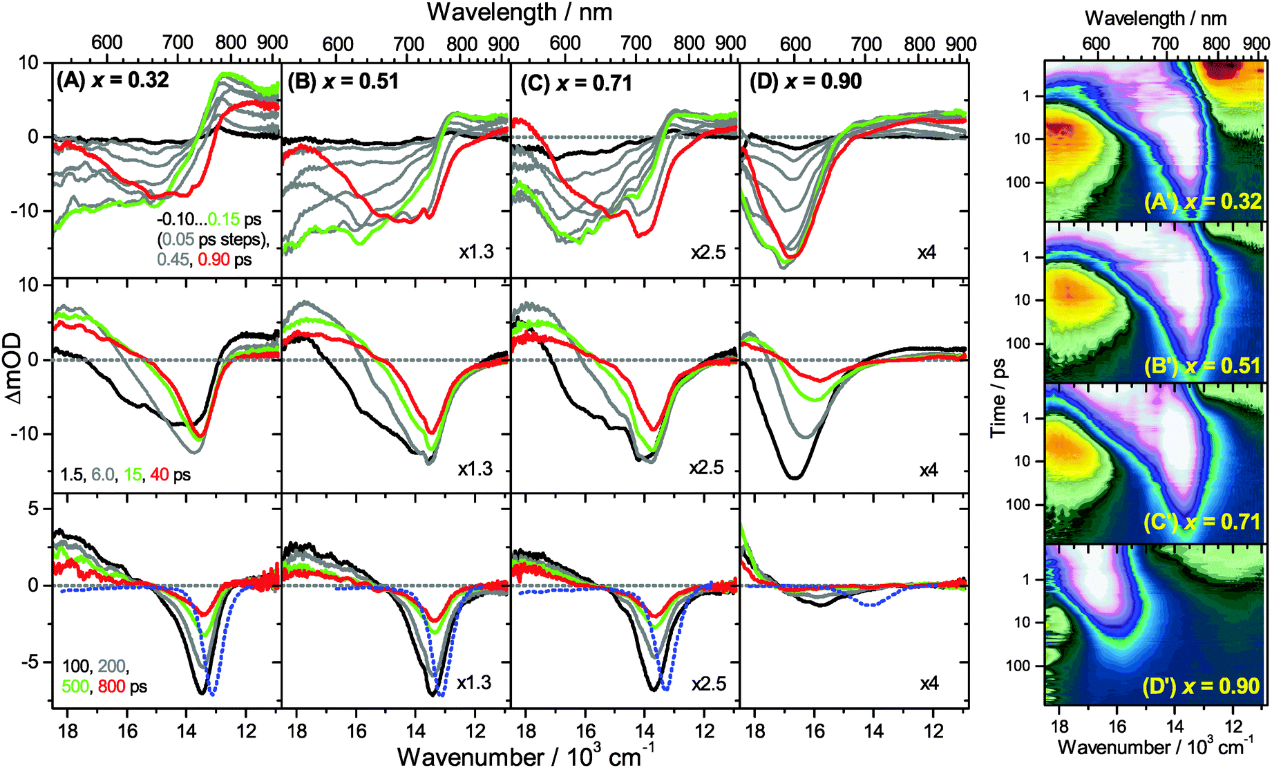 | ||
| Fig. 4 Transient Vis-NIR PSCP broadband absorption spectra of (MAI)x(PbI2)1−x/TiO2/glass at a pump pulse fluence of 50 μJ cm−2 for different initial mole fractions x. Columns (A) to (D) are the results for x = 0.32, 0.51, 0.71 and 0.90, respectively. (top panels) −0.10…0.15 ps with 50 fs steps; 0.45 ps, 0.90 ps; (middle panels) 1.5, 6.0, 15 and 40 ps; (bottom panels) 100, 200, 500 and 800 ps. Selected transient spectra are shown as thick colored lines for guidance. The blue-dotted lines in the bottom panels are the scaled steady-state stimulated emission spectra. (A′–D′) Show the dynamics of the systems in (A–D) as contour plots using a logarithmic time scale. White, pink and bluish colors denote bleach or stimulated emission, whereas green, yellow and red colors correspond to transient absorption. | ||
 | ||
| Fig. 5 Kinetic traces extracted from transient PSCP broadband absorption spectra for (MAI)x(PbI2)1−x/TiO2/glass samples. Panels (A–D) are for x = 0.32, 0.51, 0.71 and 0.90, respectively. Black and green lines are for 2 and 50 μJ cm−2 fluence at λprobe = 600 nm. Blue and red lines represent 2 and 50 μJ cm−2 fluence at λprobe = 750 nm. | ||
We commence with the data at low pump beam fluence for x = 0.32, 0.51 and 0.71, shown in Fig. 3(A–C). The dynamics in this range of mole fractions look quite similar. Obviously, at least in this spectral range, the PbI2 enrichment inside the x = 0.32 sample and the contribution of SPS for x = 0.71 do not influence the transient spectra dramatically, and the carrier dynamics are quite unaffected, which is an important result for device performance, as an accurate choice of mole fraction does not seem to be so critical. The early-time dynamics up to 0.9 ps (top panel) show that the initially extended tail of the carrier distribution in the 500–750 nm range changes from a flat to a steeper slope, see the green and red lines. According to our previous analysis and in agreement with the existing body of literature on carrier cooling in semiconductors,30 we assign this process to efficient carrier relaxation due to fast carrier–carrier scattering (at very early times) and slower carrier–optical phonon scattering at later times.15 We extract a time constant of ca. 300 fs for carrier–optical phonon scattering at 625 nm, where the decay due to cooling is most pronounced. In addition, we observe a clear sub-band gap absorption feature around 785 nm which decays with a time constant of 300 fs. It arises from a typical band-gap renormalization effect, as discussed previously for MAPbI3.15,31
For the experiments at an about 25 times larger fluence, the early-time carrier distribution is considerably broader and therefore possesses a higher quasi-temperature, see Fig. 4(A–C). In addition, cooling is significantly slower, when comparing e.g. in Fig. 3(A–C) and 4(A–C) the spectra at 0.9 ps (top panels) and the spectra at 1.5 ps (middle panels). We extract a time constant of 2.8 ps at 625 nm (1.5 ps for the experiments at intermediate pump fluence). In addition, a slower decay is observed for the sub-bandgap absorption (ca. 550 fs), which also extends further into the NIR at higher pump fluences. The slower cooling arises from the different time scales of carrier–carrier and carrier–phonon scattering. Therefore, at high initial carrier densities, the cooling via optical phonons is less efficient. This behavior is typically denoted as the “hot phonon effect” or “phonon bottleneck”, which is well known for semiconductors and zero-bandgap materials, such as graphene.32 The slightly higher NIR absorption at longer times for the x = 0.32 sample in Fig. 4(B) above 800 nm might be interpreted as weak absorption of PbI2, based on the transient absorption spectra of pure PbI2 previously recorded by us.15
The carrier temperature may be modelled by a simple fit of the high energy tail of the bleach feature to an expression proportional to E2·exp[−E/(kB·Tcarrier)], similar to the approach employed by Kash et al. for InGaAs.27 More details regarding the fitting procedure are provided in our previous paper on MAPbI3.15 Fit examples for x = 0.51 employing the normalized transient absorption data at 2 and 50 μJ cm−2 pump beam fluence are shown in Fig. 6(A) and (B), respectively. Reasonable Boltzmann fits for assigning a carrier quasi-temperature are possible starting from ca. 0.3 ps. For the low fluence case (A), the carrier temperature quickly decreases with increasing time, dropping from ca. 1100 K at 0.3 ps to 600 K at 0.5 ps and already 400 K at ca. 2 ps. The remaining excess energy is more slowly dissipated via acoustic phonons, and at 400 ps the 296 K starting temperature is re-established. The behavior is in sharp contrast to the high fluence case in (B), where initially the carrier distribution is much more extended, and relaxation is much slower. For instance, the spectra at 2 ps (magenta) in (B) provide a carrier quasi-temperature of 1100 K, similar to the red spectrum at 0.3 ps in (A). Therefore, cooling at high carrier densities progresses much slower, in agreement with the time constants mentioned above.32 Temperatures in (B) are still higher than in (A) at 400 ps (around 360 K). Cooling via acoustic phonon relaxation (heat transfer) is thus still not finished, as observed in our previous study at high fluence conditions.15 We also note that a Burstein–Moss effect is visible in our spectra as an additional contribution to the photobleach at the band edge, which adds to band broadening, as previously discussed by Manser et al.33
 | ||
| Fig. 6 Normalized transient PSCP broadband absorption spectra of (MAI)x(PbI2)1−x/TiO2/glass (x = 0.51) for (A) 2 μJ cm−2 pump fluence and (B) 50 μJ cm−2 pump fluence. (red) 0.3 ps, (orange) 0.5 ps, (grey) 1 ps, (magenta) 2 ps, (grey) 5 ps, (green) 10 ps, (grey) 100 ps and (blue) 400 ps. Dashed coloured lines denote fits to the Boltzmann tail of the carrier distribution by the procedure described in the text, resulting in the carrier quasi-temperatures provided in the figure. For higher pump fluence, carrier cooling is slowed down significantly due to the “hot phonon effect”. | ||
Moreover, the transient absorption feature below 700 nm deserves further discussion. It is observed in the middle and bottom panels of Fig. 3 and 4(A–C), after substantial carrier cooling has taken place. This spectral feature has been the subject of some debate. Previous experiments favored the presence of transient absorption from a charge-transfer excited state which was however not further specified.34 In another study, the feature was assigned to photoinduced reflection arising from a transient refractive index change of MAPbI3.20 We noted earlier that the absorption features over the whole transient spectrum in the range 320–920 nm closely resemble the shape of the first derivative of the steady-state absorption spectrum of MAPbI3.15 This would be consistent with a photoinduced transient red-shift which could be generated by a number of processes, as e.g. a transient local electric field in the material,22,31,35–38 renormalization of electron and hole states by the transient carrier populations or from lattice heating.39,40 It remains to be seen which one among these processes is operative in MAPbI3.
Turning to the long-time dynamics (bottom panels of (A–C) in Fig. 3 and 4), we observe a decay of the bleach and absorption bands, with an isosbestic point forming at ca. 680 nm (at a somewhat higher value of 705 nm for x = 0.51). The decay is the result of free carrier recombination. Kinetic traces at 600 and 750 nm are shown in Fig. 5(A–C) for pump beam fluences of 2 and 50 μJ cm−2. The recombination kinetics will be dealt with in more detail in Section 3.5 together with those of the LDP structures. We note that the bleach at 800 ps is still located at slightly shorter wavelength than the steady-state stimulated emission (SE) spectrum (blue-dotted line). We believe that the higher-wavelength part of the “bleach” feature therefore contains a sizable contribution of SE.
3.4 Charge carrier dynamics in low-dimensional perovskites
A distinctly different behavior is observed for the sample with x = 0.90, consisting mainly of low-dimensional perovskites. Results are included in Fig. 3, 4 and Fig. S3(D and D′) (ESI†). Kinetic traces are included in Fig. 5(D). In Fig. 3(D, D′) (low fluence) we observe the fast build-up (time constant 200 fs) of a bleach feature at 600 nm, i.e. 160 nm shifted to the blue compared to the perovskite materials employing lower mole fraction x. In addition, there is a clear absorption feature on the short-wavelength-side of the bleach. Over time, both bleach and absorption progressively shift to larger wavelength (time constants 7 and 50 ps). At the same time, the signal decays as a whole, and this happens much faster than for the samples with lower mole fraction x. This is due to faster carrier recombination and will be discussed separately in Section 3.5. Also there is a huge difference between the position of the bleach minimum (630 nm) and the minimum of the SE (708 nm). In addition, the bleach and SE bands are much wider. Both effects are in marked contrast to the spectral behavior of the samples employing smaller mole fractions x.We interpret the strong overall blue-shift of the bleach feature as an indication of quantum confinement due to the reduced dimensionality of the perovskite structure. Such behavior was observed previously in the case of exfoliated 2D lead iodide perovskite quantum well (QW) structures.41 Our blue-shift corresponds approximately to that of the n = 3 QW reported by Wu et al. In addition, a similar absorption feature on the blue side is observed in their QW transient absorption spectrum. The QW emission spectrum is however much sharper. This is understandable, because we obviously have a distribution of such 2D structures, possibly including also some fraction of 1D (chain) and 0D (quantum dot) structures which all absorb/emit at slightly different energies. This results in inhomogeneous spectral broadening. The strongly red-shifted emission may be assigned to emission from trap states, again in agreement with the QW results.42
Our spectra at high and intermediate fluences (Fig. 4(D, D′) and Fig. S3 (D, D′), ESI†) show similar trends. However, as one important difference, the spectral decay due to recombination is much faster. This will be modelled in Section 3.5. Another difference refers to the bleach feature which is initially much broader. We assign this to the higher quasi-temperature of the carriers, similar to the situation observed in Fig. 6. This is confirmed by the analysis of the carrier temperature of the LDP spectra in Fig. 7(A) and (B). As the band-gap in the LDPs appears to be much larger (compare the strongly blue-shifted bleach), carriers are initially prepared with less excess energy in the conduction band. Therefore, for the low fluence case in (A), we see barely a cooling effect (from 320 K at 0.3 ps to 296 K at long times). After excitation at high fluence, the carriers are initially much hotter (950 K at 0.3 ps), but they also quickly cool down to 310 K within 10 ps.
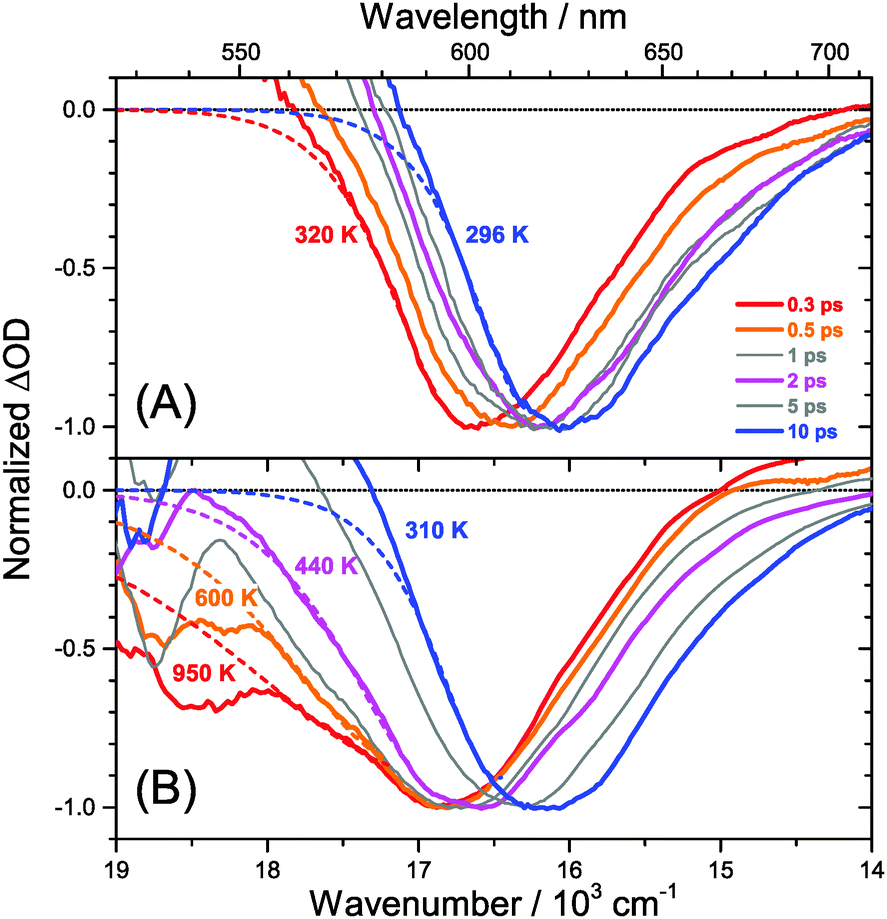 | ||
| Fig. 7 Normalized transient PSCP broadband absorption spectra of (MAI)x(PbI2)1−x/TiO2/glass (x = 0.90) for (A) 2 μJ cm−2 pump fluence and (B) 50 μJ cm−2 pump fluence. (red) 0.3 ps, (orange) 0.5 ps, (grey) 1 ps, (magenta) 2 ps, (grey) 5 ps and (blue) 10 ps. Dashed coloured lines represent fits to the Boltzmann tail of the carrier distribution by the procedure described in the text, resulting in the carrier quasi-temperatures provided in the figure. For higher pump fluences, carrier cooling is substantially slower. | ||
3.5 Electron–hole recombination dynamics
The general rate expression for carrier recombination considers three terms of first, second and third order:43 | (1) |
We treat the kinetics by the standard expression for a bimolecular process A + B (electron + hole) with equal initial number densities of electrons and holes (n0 = ne = nh, in cm−3), similar to the approach of Manser et al.:33
 | (2) |
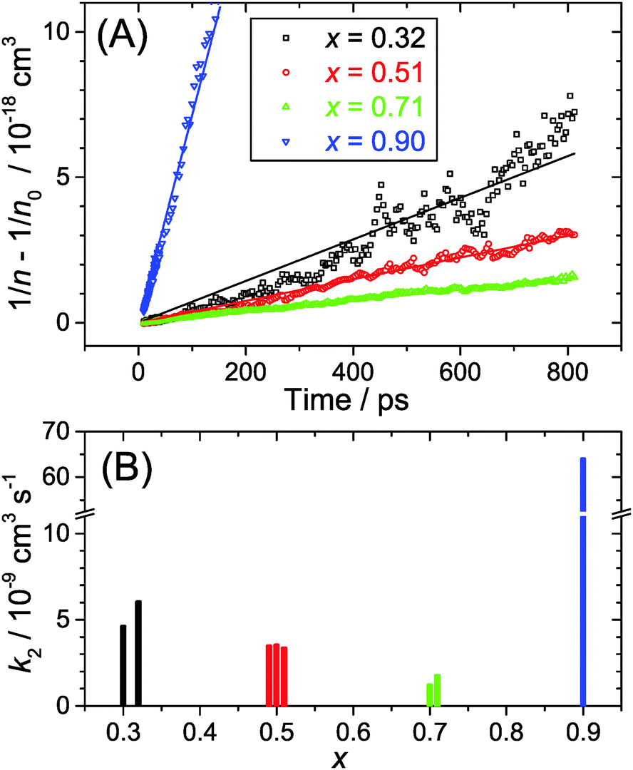 | ||
| Fig. 8 (A) Plot of the difference of the reciprocal transient (n) and initial (n0) carrier density as a function of time for the (MAI)x(PbI2)1−x/TiO2/glass samples employing MAI mole fractions x = 0.32 (black), 0.51 (red), 0.71 (green) and 0.90 (blue). The slope corresponds to the second-order rate constant k2 for electron–hole recombination, which is more than one order of magnitude larger for low-dimensional perovskites (x = 0.90). The data and fits in the plots are for high pump fluence (50 μJ cm−2). (B) Plot of the second-order rate constant k2 as a function of the MAI mole fraction x for multiple determinations. Note the break on the k2 axis. | ||
4. Conclusions
In the current study, we presented detailed experiments of the ultrafast carrier dynamics of the (MAI)x(PbI2)1−x system using pump-supercontinuum probe spectroscopy, where excitation was performed at 500 nm. The variation of the mole fraction of methylammonium iodide in the range x = 0.32–0.71 results in a systematic reduction of the carrier recombination rate constant k2 from 5.3 × 10⁻⁹ to 1.5 × 10⁻⁹ cm3 s−1. In any case, the good carrier transport properties of these solution-processed semiconductors are not compromised. Efficient carrier cooling on a 300 fs time scale was observed after excitation at low fluences of 2 μJ cm−2, and this relaxation slowed down considerably to ca. 2.8 ps at high fluences of 50 μJ cm−2. This may be explained by the “hot phonon effect”.Drastic changes are seen for x = 0.90. At such a high excess of MAI, low-dimensional perovskite (LDP) structures are formed which behave very different. The steady-state luminescence is considerably blue-shifted as are the bleach features in the transient spectra. This can be traced back to quantum confinement effects in the low-dimensional structures. The second-order rate constant for electron–hole recombination is by more than one order of magnitude larger in LDPs than in the other perovskite structures studied, but still in an acceptable regime that construction of solar cells or LED devices should be feasible.
Acknowledgements
KO and TL thank the German Science Foundation (DFG) for financial support of this work through grants OU 58/10-1 and LE 926/11-1. XRD data were kindly provided by T. Kowald and H. F. Trettin (University of Siegen). We also thank J. Weber and J. Schmedt auf der Günne (University of Siegen) for providing the oven for sintering the mesoporous TiO2 layers. Continuous support and advice by J. Troe, D. Schwarzer, K. Luther, J. Schroeder, A. M. Wodtke (Georg August University Göttingen, Germany), as well as N. P. Ernsting (Humboldt University Berlin, Germany) and J. L. Pérez Lustres (University of Santiago de Compostela, Spain) are gratefully acknowledged.Notes and references
- N.-G. Park, Mater. Today, 2015, 18, 65 CrossRef CAS.
- H. J. Snaith, J. Phys. Chem. Lett., 2013, 4, 3623 CrossRef CAS.
- H. S. Jung and N.-G. Park, Small, 2015, 11, 10 CrossRef CAS PubMed.
- N.-G. Park, J. Phys. Chem. Lett., 2013, 4, 2423 CrossRef CAS.
- S. Kazim, M. K. Nazeeruddin, M. Grätzel and S. Ahmad, Angew. Chem., Int. Ed., 2014, 53, 2812 CrossRef CAS PubMed.
- C. R. Kagan, D. B. Mitzi and C. D. Dimitrakopoulos, Science, 1999, 286, 945 CrossRef CAS PubMed.
- Z.-K. Tan, R. S. Moghaddam, M. L. Lai, P. Docampo, R. Higler, F. Deschler, M. Price, S. Sadhanala, L. M. Pazos, D. Credgington, F. Hanusch, T. Bein, H. J. Snaith and R. H. Friend, Nat. Nanotechnol., 2014, 9, 687 CrossRef CAS PubMed.
- O. Malinkiewicz, A. Yella, Y. H. Lee, G. Mínguez Espallargas, M. Grätzel, M. K. Nazeeruddin and H. J. Bolink, Nat. Photonics, 2014, 8, 128 CrossRef CAS.
- D. B. Mitzi, J. Mater. Chem., 2004, 14, 2355 RSC.
- I. C. Smith, E. T. Hoke, D. Solis-Ibarra, M. D. McGehee and H. I. Karunadasa, Angew. Chem., Int. Ed., 2014, 53, 11232 CrossRef CAS PubMed.
- E. R. Dohner, E. T. Hoke and H. I. Karunadasa, J. Am. Chem. Soc., 2015, 136, 1718 CrossRef PubMed.
- Z. Song, S. C. Watthage, A. B. Phillips, B. L. Tompkins, R. J. Ellingson and M. J. Heben, Chem. Mater., 2015, 27, 4612 CrossRef CAS.
- K. Xiong, W. Liu, S. J. Teat, L. An, H. Wang, T. J. Emge and J. Li, J. Solid State Chem., 2015, 230, 143 CrossRef CAS.
- D. H. Cao, C. C. Stoumpos, O. K. Farha, J. T. Hupp and M. G. Kanatzidis, J. Am. Chem. Soc., 2015, 137, 7843 CrossRef CAS PubMed.
- O. Flender, J. R. Klein, T. Lenzer and K. Oum, Phys. Chem. Chem. Phys., 2015, 17, 19238 RSC.
- J. H. Heo, S. H. Im, J. H. Noh, T. N. Mandal, C.-S. Lim, J. A. Chang, Y. H. Lee, H.-j. Kim, A. Sarkar, M. K. Nazeeruddin, M. Grätzel and S. I. Seok, Nat. Photonics, 2013, 7, 486 CrossRef CAS.
- J.-H. Im, C.-R. Lee, J.-W. Lee, S.-W. Park and N.-G. Park, Nanoscale, 2011, 3, 4088 RSC.
- J.-H. Im, I.-H. Jang, N. Pellet, M. Grätzel and N.-G. Park, Nat. Nanotechnol., 2014, 9, 927 CrossRef CAS PubMed.
- J. Burschka, N. Pellet, S.-J. Moon, R. Humphry-Baker, P. Gao, M. K. Nazeeruddin and M. Grätzel, Nature, 2013, 499, 316 CrossRef CAS PubMed.
- M. B. Price, J. Butkus, T. C. Jellicoe, A. Sadhanala, A. Briane, J. E. Halpert, K. Broch, J. M. Hodgkiss, R. H. Friend and F. Deschler, Nat. Commun., 2015, 6, 8420 CrossRef CAS PubMed.
- F. Ehlers, M. Scholz, J. Schimpfhauser, J. Bienert, K. Oum and T. Lenzer, Phys. Chem. Chem. Phys., 2015, 17, 10478 RSC.
- K. Oum, P. W. Lohse, O. Flender, J. R. Klein, M. Scholz, T. Lenzer, J. Du and T. Oekermann, Phys. Chem. Chem. Phys., 2012, 14, 15429 RSC.
- P. W. Lohse, J. Kuhnt, S. I. Druzhinin, M. Scholz, M. Ekimova, T. Oekermann, T. Lenzer and K. Oum, Phys. Chem. Chem. Phys., 2011, 13, 19632 RSC.
- K. Golibrzuch, F. Ehlers, M. Scholz, R. Oswald, T. Lenzer, K. Oum, H. Kim and S. Koo, Phys. Chem. Chem. Phys., 2011, 13, 6340 RSC.
- T. Lenzer, S. Schubert, F. Ehlers, P. W. Lohse, M. Scholz and K. Oum, Arch. Biochem. Biophys., 2009, 483, 213 CrossRef CAS PubMed.
- A. L. Dobryakov, S. A. Kovalenko, A. Weigel, J. L. Pérez Lustres, J. Lange, A. Müller and N. P. Ernsting, Rev. Sci. Instrum., 2010, 81, 113106 CrossRef CAS PubMed.
- K. Kash and J. Shah, Appl. Phys. Lett., 1984, 45, 401 CrossRef CAS.
- J. A. Sichert, Y. Tong, N. Mutz, M. Vollmer, S. Fischer, K. Z. Milowska, R. García Cortadella, B. Nickel, C. Cardenas-Daw, J. K. Stolarczyk, A. S. Urban and J. Feldmann, Nano Lett., 2015, 15, 6521 CrossRef CAS PubMed.
- P. Tyagi, S. M. Arveson and W. A. Tisdale, J. Phys. Chem. Lett., 2015, 6, 1911 CrossRef CAS PubMed.
- J. Shah, Ultrafast Spectroscopy of Semiconductors and Semiconductor Nanostructures, Springer, Berlin, 1999 Search PubMed.
- K. Chen, A. J. Barker, F. L. C. Morgan, J. E. Halpert and J. M. Hodgkiss, J. Phys. Chem. Lett., 2014, 6, 153 CrossRef PubMed.
- L. Huang, B. Gao, G. Hartland, M. Kelly and H. Xing, Surf. Sci., 2011, 605, 1657 CrossRef CAS.
- J. S. Manser and P. V. Kamat, Nat. Photonics, 2014, 6, 737 CrossRef.
- K. G. Stamplecoskie, J. S. Manser and P. V. Kamat, Energy Environ. Sci., 2015, 8, 208 CAS.
- V. I. Klimov, in Semiconductor Nanocrystals – From Basic Principles to Applications, ed. A. L. Efros, D. J. Lockwood and L. Tsybeskov, Springer, New York, 2003, p. 73 Search PubMed.
- K. Oum, P. W. Lohse, J. R. Klein, O. Flender, M. Scholz, A. Hagfeldt, G. Boschloo and T. Lenzer, Phys. Chem. Chem. Phys., 2013, 15, 3906 RSC.
- K. Oum, O. Flender, P. W. Lohse, M. Scholz, A. Hagfeldt, G. Boschloo and T. Lenzer, Phys. Chem. Chem. Phys., 2014, 16, 8019 RSC.
- M. Fakis, P. Hrobárik, O. Yushchenko, I. Sigmundová, M. Koch, A. Rosspeintner, E. Stathatos and E. Vauthey, J. Phys. Chem. C, 2014, 118, 28509 CAS.
- K. Oum, T. Lenzer, M. Scholz, D. Y. Jung, O. Sul, B. J. Cho, J. Lange and A. Müller, J. Phys. Chem. C, 2014, 118, 6454 CAS.
- K. Seibert, G. C. Cho, W. Kütt, H. Kurz, D. H. Reitze, J. I. Dadap, H. Ahn, M. C. Downer and A. M. Malvezzi, Phys. Rev. B: Condens. Matter Mater. Phys., 1990, 42, 2842 CrossRef CAS.
- X. Wu, M. T. Trinh and X.-Y. Zhu, J. Phys. Chem. C, 2015, 119, 14714 CAS.
- X. Wu, M. T. Trinh, D. Niesner, H. Zhu, Z. Norman, J. S. Owen, O. Yaffe, B. J. Kudisch and X.-Y. Zhu, J. Am. Chem. Soc., 2015, 137, 2089 CrossRef CAS PubMed.
- R. L. Milot, G. E. Eperon, H. J. Snaith, M. B. Johnston and L. M. Herz, Adv. Funct. Mater., 2015, 25, 6218 CrossRef CAS.
- G. Xing, N. Mathews, S. Sun, S. S. Lim, Y. M. Lam, M. Grätzel, S. Mhaisalkar and T. C. Sum, Science, 2013, 342, 344 CrossRef CAS PubMed.
- C. Wehrenfennig, G. E. Eperon, M. B. Johnston, H. J. Snaith and L. M. Herz, Adv. Mater., 2014, 26, 1584 CrossRef CAS PubMed.
Footnote |
| † Electronic supplementary information (ESI) available: Changes of XRD patterns for x = 0.71 upon annealing; optimized annealing condition monitored by XRD; transient Vis-NIR spectra at the pump fluence 14 μJ cm−2; analysis of recombination kinetics. See DOI: 10.1039/c5cp07167d |
| This journal is © the Owner Societies 2016 |