 Open Access Article
Creative Commons Attribution 3.0 Unported Licence
Exploring and controlling intrinsic defect formation in SnO2 thin films†
Yoann
Porte
a,
Robert
Maller
a,
Hendrik
Faber
b,
Husam N.
AlShareef
c,
Thomas D.
Anthopoulos
b and
Martyn A.
McLachlan
*a
aDepartment of Materials and Centre for Plastic Electronics, Imperial College London, London SW7 2AZ, UK. E-mail: martyn.mclachlan@imperial.ac.uk
bDepartment of Physics and Centre for Plastic Electronics, Imperial College London, London SW7 2BP, UK
cMaterials Science and Engineering, King Abdullah University of Science and Technology (KAUST), Thuwal 23955-6900, Saudi Arabia
First published on 15th December 2015
Abstract
By investigating the influence of key growth variables on the measured structural and electrical properties of SnO2 prepared by pulsed laser deposition (PLD) we demonstrate fine control of intrinsic n-type defect formation. Variation of growth temperatures shows oxygen vacancies (VO) as the dominant defect which can be compensated for by thermal oxidation at temperatures >500 °C. As a consequence films with carrier concentrations in the range 1016–1019 cm−3 can be prepared by adjusting temperature alone. By altering the background oxygen pressure (PD) we observe a change in the dominant defect – from tin interstitials (Sni) at low PD (<50 mTorr) to VO at higher PD with similar ranges of carrier concentrations observed. Finally, we demonstrate the importance of controlling the composition target surface used for PLD by exposing a target to >100![[thin space (1/6-em)]](https://www.rsc.org/images/entities/char_2009.gif) 000 laser pulses. Here carrier concentrations >1 × 1020 cm−3 are observed that are associated with high concentrations of Sni which cannot be completely compensated for by modifying the growth parameters.
000 laser pulses. Here carrier concentrations >1 × 1020 cm−3 are observed that are associated with high concentrations of Sni which cannot be completely compensated for by modifying the growth parameters.
Introduction
Transparent conducting oxides (TCOs) are currently implemented extensively in a wide variety of optoelectronic applications including; flat-panel displays, solar-cells, light-emitting diodes and thin film transistors.1–4 Whilst the development of n-type TCOs have been thoroughly investigated e.g. indium tin oxide (ITO), aluminium doped zinc oxide (AZO), and indium doped zinc oxide (IZO)5–7 the progress towards developing p-type analogues is significantly lacking, owing to the challenge of obtaining stable p-type characteristics. SnO2 is an intrinsic n-type semiconductor with a wide direct band gap (3.6 eV), high optical transparency and compatibility with a range of deposition methods. SnO2 is perhaps the material that underpins current n-type TCO technology with fluorine doped tin oxide (FTO), antimony doped tin oxide (ATO) and ITO being the most commonly implemented materials. In its stoichiometric form SnO2 is an insulator,8 however the presence of intrinsic defects creates charge carriers at concentrations large enough to ensure high conductivity. The exact nature of these defects has been the focus of numerous discussions, e.g. Kılıç and Zunger recently calculated that the low formation energy donor type defects of tin interstitials (Sni) and oxygen vacancies (VO) explain the n-type behaviour9 – specifically Sni was identified as the majority defect. This has been questioned by Godinho et al.8 who calculated VO to have a lower formation energy than Sni, which was attributed to the dual valence of tin. As a consequence, the reduction of Sn4+ to Sn2+ can occur and facilitate the formation of VO. However, Sni and VO are not the only defects responsible for n-type conductivity in SnO2. It has been shown by Kılıç and Zunger10 and Singh et al.11 that hydrogen incorporation into interstitial sites and substitution onto oxygen sites can explain the observed behaviour – this is consistent with H-donors being attributed to n-type conductivity in other oxide semiconductor systems e.g. ZnO.12,13Although n-type SnO2 is well understood, investigation of p-type conductivity in SnO2 is still challenging and has been investigated intensely over the past decade. Several reports of p-type SnO2 have been made where extrinsic dopants with a lower valence than Sn4+e.g. Al,14,15 Ga16,17 and Zn18 have been incorporated into the structure. The underlying principle lies on substituting such cations on the Sn site to induce the formation of one (or more) hole(s). Although some examples of p-type conductivity have been reported the achieved electronic properties do not reach those necessary for TCO applications. The efficiency of the p-type doping is limited in SnO2 due to self-compensation effect leading to a charge neutrality limit.19 Furthermore the high dopant concentration required to overcome the charge compensation, i.e. between 10–20 atomic percent (at%), is significantly greater than that required to achieve good n-type behaviour, e.g. 2 at% for Sb.20 When considering the possibility of demonstrating good p-type characteristics it is critical to consider controlling defect formation to avoid any impurities or n-type defects susceptible to disrupt the formation of p-type defects. The majority of existing studies conducted on p-type SnO2 do not highlight the importance of establishing “p-type compatible” conditions to ensure efficient and effective doping that allow for an understanding of the formation of intrinsic defects responsible for n-type conductivity in SnO2.
In the current study we focus on the influence of the deposition environment and growth parameters in order to control the intrinsic defects of the SnO2 system. Our chosen growth technique, pulsed laser deposition (PLD), is particularly suitable for this investigation as it facilitates excellent cation transfer from the target materials, allows deposition under a wide range of oxygen pressures21 (PD) (thus control of electrical conductivity), supports high deposition rates and allows excellent control of the film growth parameters.22 We present our results in three parts, describing first the independent variation of deposition temperature (TD) and PD and then where the PLD target is changed through multiple interactions with the laser i.e. growth cycles. The experimentally measured properties of our thin films are discussed with consideration to the numerous theoretical calculations contained in the literature to determine the role of donor type defects in SnO2.
Results and discussion
For the studies where TD was varied the PD was fixed at 100 mTorr we investigated the variation of TD over the range 300–700 °C. In the case of PD variation TD was maintained at 600 °C and PD changed from 5–300 mTorr (0.67–40 Pa). For the target exposure variation our ceramic target was pre-exposed to >100![[thin space (1/6-em)]](https://www.rsc.org/images/entities/char_2009.gif) 000 laser pulses and films then deposited under the same conditions as those prepared when varying TD and PD. A commercial SnO2 target was used owing to the difficulties of sintering dense (∂ > 95%) targets in-house without the use of additives that may contribute to doping.23
000 laser pulses and films then deposited under the same conditions as those prepared when varying TD and PD. A commercial SnO2 target was used owing to the difficulties of sintering dense (∂ > 95%) targets in-house without the use of additives that may contribute to doping.23
Influence of deposition temperature (TD)
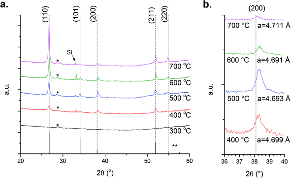
The films grown exhibit mainly the casserite phase (SnO2) with some evidence of SnO being present, shown by the typical X-ray diffraction (XRD) data in Fig. 1a. At 300 °C the films are amorphous with crystalline films deposited at all other temperatures. The crystalline films exhibit a strong (110) orientation with diffraction from the (101), (200) and (211) planes observed to differing extents consistent with other reports.24 To quantise the preferential orientation of our films the texture coefficient TC(hkl) was calculated using the eqn (1):25 | (1) |
![[thin space (1/6-em)]](https://www.rsc.org/images/entities/char_2009.gif) sin
sin![[thin space (1/6-em)]](https://www.rsc.org/images/entities/char_2009.gif) θ):
θ): | (2) |
The calculated a-lattice parameter shows a reduction as T increases from 400–600 °C but then increases when T is increased further, Fig. 1b. Such changes are indicative of intrinsic defects in the films. While Sni, oxygen interstitials (Oi) or doubly charged oxygen vacancies  increase the size of the lattice VO induces a reduction in lattice size.11
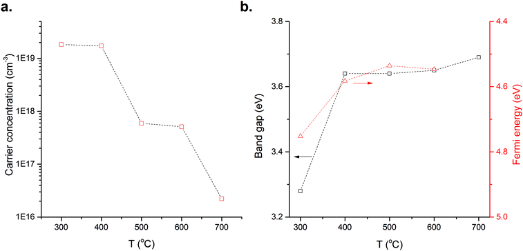
The measured film carrier concentrations are shown in Fig. 2a, the data show a clear reduction in the n-type carrier concentration by some three-orders of magnitude as TD is increased. This suggests that the concentration of either Sni or VO do not rise with TD, as these are well-known n-type donor defects. The evolution of the optical band gap (Eg) and the Fermi level (EF) as temperature is varied are shown in Fig. 2b. The Eg values above 400 °C are around 3.6 eV which is consistent with previous reports,26 with the low value of 3.2 eV at 300 °C being attributed to band tailing effects present in amorphous films.27 Similarly the increase in EF as TD is increased from 300 to 400 °C is also attributed to the band tailing effects, Fig. 2b. The EF position is a product of electron chemical potential and surface dipole.28 While the surface dipole is affected by the surface roughness29–31 and the exposed crystal surface32 we assume that these remain constant over the range of TD investigated and that any contribution from surface dipole is negligible compared with the electron chemical potential which is directly influenced by the phase and structure of the materials, its stoichiometry and the presence of impurities and/or intrinsic/extrinsic defects.33 More precisely, the presence of either intrinsic or extrinsic defects is known to directly influence the position of the EF![[thin space (1/6-em)]](https://www.rsc.org/images/entities/char_2009.gif) 28,34,35 that can form additional occupied or unoccupied states within the Eg altering the carrier concentration and shifting the EF within the band gap. In Fig. 3 the energy levels of several crystalline defects in the SnO2 system are shown. This diagram gathers the defect transition energy levels, ε(q/q′) where q and q′ are two charge states of the defect, extracted from literature calculations. In most models used in such calculations, i.e. local-density approximation (LDA)9 or the hybrid density functional theory (DFT),36 the value of the band gap is underestimated and the energy level of these defects may vary. Therefore the defects energies represented in Fig. 3 are an approximation of where such levels lie.
28,34,35 that can form additional occupied or unoccupied states within the Eg altering the carrier concentration and shifting the EF within the band gap. In Fig. 3 the energy levels of several crystalline defects in the SnO2 system are shown. This diagram gathers the defect transition energy levels, ε(q/q′) where q and q′ are two charge states of the defect, extracted from literature calculations. In most models used in such calculations, i.e. local-density approximation (LDA)9 or the hybrid density functional theory (DFT),36 the value of the band gap is underestimated and the energy level of these defects may vary. Therefore the defects energies represented in Fig. 3 are an approximation of where such levels lie.
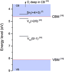 | ||
| Fig. 3 Schematic representation of defect transition levels in SnO2 in the form D(q/q′) where D is the defect, q the charge of the defect below the transition level and q′ the charge above it (values extracted from ref. 7, 33 and 40. Valence band (VB) and conduction band (CB) represented in blue blocks. The valence band maximum (VBM) and the conduction band minimum (CBM) are represented by a red line (values from ref. 22). | ||
The charge of the defect is defined by the position of the EF and the transition energy level of the defect ε(q/q′). VO has a donor level 0.115 eV below the conduction band minima (CBM) for εVO(+2/0)9 and ionisation will only occur if the EF lies below this level, otherwise the defect remains neutral. If we consider the CBM to be around 4.6 eV22 the energy of εVO(+2/0) will be ∼4.7 eV. Measurements of EF, Fig. 2b, show that at TD above 400 °C values lie above 4.6 eV i.e. above the CB minima, thus the VO present are likely to be in neutral state hence their contribution to change in electrical properties would be negligible and another defect must be responsible for the observed reduction in carrier concentration as TD increases. More likely is a decrease in Sni which would explain both the reduction in a-lattice parameter and the fall in carrier concentration observed between 300 and 600 °C. The increase of the a-lattice parameter at 700 °C may be due to a reduction in VO which, based on the Ef position, should be in a neutral charge state consequently inducing a compression of the lattice.11 Other defects i.e. Oi or tin vacancies (VSn) may be present however the high substrate temperature may provide sufficient energy for Sn species in the plume to react with O and bring the system closer to stoichiometry. The presence of VSn in SnO2 thin films has been previously discussed,37–39 however there presence in large concentrations has been ruled out owing to their high formation energy.37
Under the range of TD investigated the presence of either tin or oxygen antisites are ruled out owing to their high formation energies.36 Ke et al. studied the effect of annealing temperature in pure oxygen40 where they observed an oxidation of the films above 500 °C leading to a decrease of VO. It should be noted that the growth environment in our study differs from that reported by Ke et al. hence we suggest a qualitative rather than quantitative comparison.
Therefore it may be logical to attribute the observed reduction in carrier concentration to a reduction of Sni and VO through oxidation i.e. as TD increases Sn has enough energy to fully react with molecular oxygen, leading to the formation of films closer to stoichiometry which is consistent with previous reports.37 The temperature dependent variation in EF, lattice constant and electrical properties are associated directly with a reduction in n-type defect concentration.
Influence of background oxygen pressure (PD)
Films deposited at 700 °C had the lowest measured carrier concentrations, 2 × 1016 cm−3, which would appear to be the optimum TD for minimising donor defects. However owing to technical issues relating to sample mounting and subsequent analysis for variation of PD a fixed TD of 600 °C was chosen. Although 700 °C may appear to be the optimum TD for reducing n-type defects, considerations regarding the sample mounting and thermal degradation of ITO (thus directly impacting EF measurements) must be made. We suggest that 600 °C is adequate to balance processing restrictions with optimum characteristics, thus studies to elucidate the impact of PD were carried out at this temperature.The XRD data show that SnO2, Fig. 4a, films still exhibit a preferential (110) orientation, however we observe a shift in the preferred orientation as PD varies. At low PD the growth is dominated by the (101) orientation. This peak almost disappears when PD increases to 50 mTorr with a change to (110) orientated films. Further increases in PD result in the appearance of (101) and (211) preferred orientations. This is quantified through analysis of the TC, summarised in Table S2.† The behaviour observed at low PD, i.e. 5 mTorr, may be attributed to the highly energetic ablated species in the plume as a result of reduced interaction with molecular oxygen, promoting growth not supported under other conditions.22 Introduction of molecular oxygen into the chamber, i.e. for 5–50 mTorr, lead to a corresponding shift in a-lattice parameter, Fig. 4b, which may also be attributed to a decrease in the concentration of Sni defects. This is supported by Kılıç and Zunger who showed the formation energy of Sni decreases in oxygen-deficient environments.9 Consequently, the combined Sn-rich/O-poor environment would favour the formation of Sni over VO. Above 50 mTorr, the lattice parameter shows a subtle gradual increase until 200 mTorr. To understand the impact of structural variation and its origin we probe the extracted carrier concentrations in Fig. 5a, where it is shown that increasing PD over the range studied results in a three-orders of magnitude reduction in carrier concentration. This may be explained through a reduction in VO or the presence of Oi or VSn to compensate the n-type defects. The formation energies of Oi and VSn decrease under oxygen-rich conditions and the presence of these defects would contribute to the subtle increase in a-lattice parameter and with the reduction in carrier concentration. As with TD variation we consider that such defects will be present in small quantities owing to their high formation energy.36 It remains more plausible that as PD is increased, the system again approaches to stoichiometry by incorporating more oxygen, this is supported by Scanlon and Watson36 who demonstrated that the formation energy of VO and Sni increases when the environment becomes oxygen-rich.
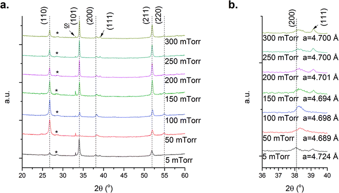 | ||
| Fig. 4 XRD data for the SnO2 films prepared at a fixed temperature of 600 °C with the oxygen pressure varied from 5–300 mTorr, symbols and dashed lines as Fig. 1, (a) SnO2, and (b) magnified analysis of the (200) diffraction peak and the calculated a-lattice parameter obtained for the films. | ||
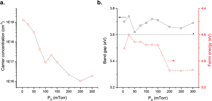 | ||
| Fig. 5 Measured electrical and optical properties of the films deposited over the background oxygen pressure range 5–300 mTorr, (a) carrier (electron) concentrations measured by AC Hall effect, (b) optical band gap calculated from Tauc analysis of UV-Vis data and measured Fermi level. *Band gap value from Batzill et al.26 | ||
The Eg values for all PD values are around 3.6–3.7 eV, Fig. 5b, with no systematic variation observed with the change in processing conditions. However, there is a sharp decrease in the EF values above 150 mTorr. This shift towards the centre of the Eg can be interpreted as support for the structure moving towards stoichiometry where in the stoichiometric state the EF of a metal oxide should lie halfway between the top of the VB and the bottom of the CB.34,35 Globally the increase in PD results in a decrease in the charge carrier concentration attributed to a reduction in the concentration of Sni and VO. Thus, the SnO2 films approach stoichiometry by limiting the amount of donor type defects. Identifying the experimental conditions at which this occurs is essential for the development of p-type SnO2i.e. it is necessary to eliminate the formation of n-type defects to avoid charge compensation when p-type defects are introduced. Based on the results presented we consider that a TD of 600 °C and a PD of 250 mTorr of oxygen are sufficient to significantly reduce the concentration of Sni and VO.
Influence of target surface composition
For PLD, the TD and the PD constitute perhaps the two most important and widely investigated parameters to vary during growth. What is often overlooked is the composition of the target before, during and after deposition – whilst the initial cation concentrations can be controlled during target preparation this value may change during laser exposure. This was exemplified by Claeyssens et al.41 who studied this in the ZnO system. Specifically, the authors observed a Zn enrichment on ablated targets due to backscattering from the plasma plume and subsequent condensation on the target surface. The least volatile component condenses first i.e. Zn, leading to the Zn rich surface. This observation partly explains why non-stoichiometric films are deposited when a target is used for extended periods. In the data presented above we have eliminated such effects by polishing the target between successive depositions. However, to fully investigate the influence of target composition changes in the SnO2 system we compare the experimental data shown previously with data obtained using an unpolished target that was subjected to >100![[thin space (1/6-em)]](https://www.rsc.org/images/entities/char_2009.gif) 000 pulses. In particular, we do so by fixing TD and varying PD over the range 5–300 mTorr.
000 pulses. In particular, we do so by fixing TD and varying PD over the range 5–300 mTorr.
Fig. 6a shows the XRD data obtained during the variation of PD using an exposed target. Similar behaviour to that observed previously for polished targets is seen at PD = 5 mTorr, with a strong preferred (101) orientation and a noticeable increase in the relative intensity of the (211) diffraction peak. Increasing PD from 50–150 mTorr results in the appearance of a strong (200) peak and a reduction in the (211) intensity. At 200 mTorr the (211) peak dominates the diffraction data and at higher PD values i.e. >250 mTorr the data for polished and unpolished targets are comparable. Changes in the XRD data with increased PD are attributed to a reduction in VO. However, when comparing the a-lattice parameters for films prepared from the exposed and polished targets it is apparent that at PD < 200 mTorr the a-lattice parameter obtained from the polished target is smaller, Fig. 6b.
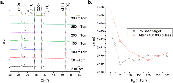 | ||
Fig. 6 XRD data for the SnO2 films prepared using a SnO2 target exposed to >100![[thin space (1/6-em)]](https://www.rsc.org/images/entities/char_2009.gif) 000 laser pulses at a fixed temperature of 600 °C with the oxygen pressure varied from 5–300 mTorr, symbols and dashed lines as Fig. 1. 000 laser pulses at a fixed temperature of 600 °C with the oxygen pressure varied from 5–300 mTorr, symbols and dashed lines as Fig. 1. | ||
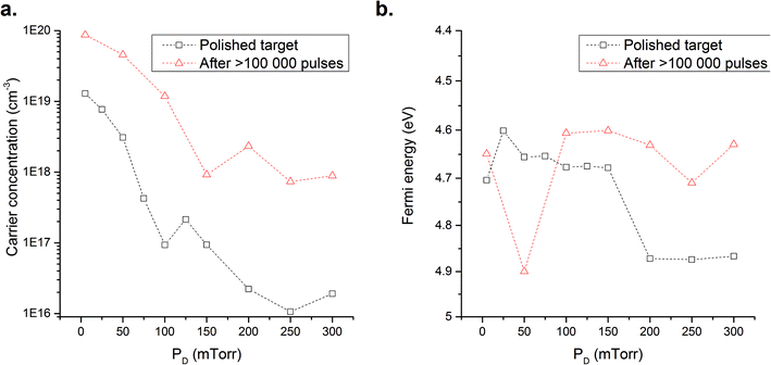
This is exemplified by examining the carrier concentrations and EF of the films prepared, Fig. 7a. The carrier concentrations for the unpolished films are significantly higher at all PD values than those prepared from a polished target. At low PD, i.e. below 100 mTorr, there is little fluctuation as PD is increased owing to the high Sni concentration that cannot be compensated for by the increased oxygen content of the chamber. Above 100 mTorr the carrier concentration falls by more than one order of magnitude as the Sni defects begin to be compensated by VO filling. However, we suggest that a significant concentration of Sni persists which accounts for the increased carrier concentrations and the larger measured a-lattice constant. Thus the combination of structural, XRD, and electrical characteristics give a direct insight into the defect species dominating the films. Similar to films prepared from polished targets those deposited from the exposed target get closer to stoichiometry as PD is increased, but even at the highest PD studied (300 mTorr) the carrier concentration of these films are some two-orders of magnitude greater than those prepared from polished targets. This highlights the issue of Sn recondensation on the target surface, the creation of an Sn rich growth environment and the resultant impact on measured electrical properties. Concerning the defects present in the films, we conclude that two effects are being observed in parallel with the unpolished target (i) an increase in Sni owing to Sn enrichment of the target surface, and (ii) a reduction in VO attributed to the increased amounts of oxygen.
Analysis of the EF position for films prepared with exposed targets shows some considerable variations, particularly at PD < 100 mTorr where the value at 50 mTorr falls to 4.9 eV compared with 4.65–4.6 eV at 5 and 100 mTorr. Whilst the 50 mTorr value may appear to be an outlier, it has been reconfirmed several times by repeat measurements. Such a shift could be characteristic of a change in defect nature within the lattice. While most of the defect energy levels have been estimated theoretically, Fig. 4, the VO energy level has been extracted experimentally by Samson and Fonstad42 to lie just below the CB minima (150 meV below in the case of the second ionized level of VO) with the CB edge established at around 4.6 eV.22 Here we suggest that the extremely high carrier concentrations and the variation in EF could be attributed to a shift of the dominant defect from Sni (energy above the CB9) toward VO. Whist this may not be intuitive we believe the increase in oxygen content in the chamber raises the formation energy of Sni above that of VO. This matter has been widely discussed by Kılıç and Zunger,9 Singh et al.11 and Godinho et al.8 where either Sni or VO form preferentially in SnO2. However the formation of a preferred defect is subject to its environment. Furthermore, as the carrier concentration of the exposed target films is maintained above 1019 cm−3, Fig. 7a, the presence of a defect other than Sni is indicated (e.g. VO) in order to ensure the formation of n-type charge carriers. Greiner et al.28 suggest a decrease of the work function as the oxidation state decreases. This would translate to the EF moving towards the CB as more VO are formed. However we believe this effect is limited by the presence of other defects such as Sni whose formation energy lies above the CB minima.
Conclusions
We report a detailed investigation of the structural and electronic properties of SnO2 films grown by pulsed laser deposition (PLD). By independently studying the growth temperature (TD) and growth chamber oxygen gas pressure (PD) we have identified growth conditions that allow significant control over intrinsic defect levels in our films. Considering TD, we show significant changes over the temperature range 300–700 °C attributed to a marked change in Sni and VO concentrations. At low temperatures, <500 °C, Sni and VO dominate the defect chemistry resulting in films with high charge carrier concentrations >2 × 1019 cm−3 reducing to 2 × 1016 cm−3 at 700 °C – associated with thermal oxidation not possible at lower temperatures.For PD variation we again observe a change in the structure associated with defect formation. In this case, deposition below 50 mTorr results in large concentration Sni rather than VO. Here the films show a near three-orders of magnitude reduction in carrier concentration when PD is increased from 50–300 mTorr associated with the removal of these n-type donor defects and a shift towards more stoichiometric SnO2. In support of this theory the measured Fermi level (EF) shift from near the conduction band towards the middle of the band-gap (Eg) at PD > 150 mTorr which is consistent with a system moving towards stoichiometry.
In the final section we consider the importance of the PLD target surface, which by exposing to >100![[thin space (1/6-em)]](https://www.rsc.org/images/entities/char_2009.gif) 000 laser pulses becomes metal rich. When TD is fixed and PD varied over the same range as previously studied carrier concentrations approaching 1 × 10²⁰ electrons per cm−3 (50 mTorr) are measured. The enrichment of Sn on the target surface significantly increases the concentration of Sni in the films – supported by the XRD data. The large concentration of Sni cannot in this case be compensated for by increasing PD, although the carrier concentration reduces with increasing PD, the EF position remains close to the conduction band indicating that Sni defects are present in large concentrations.
000 laser pulses becomes metal rich. When TD is fixed and PD varied over the same range as previously studied carrier concentrations approaching 1 × 10²⁰ electrons per cm−3 (50 mTorr) are measured. The enrichment of Sn on the target surface significantly increases the concentration of Sni in the films – supported by the XRD data. The large concentration of Sni cannot in this case be compensated for by increasing PD, although the carrier concentration reduces with increasing PD, the EF position remains close to the conduction band indicating that Sni defects are present in large concentrations.
In conclusion we show the relationship between the main processing parameters, namely TD, PD and target surface composition on the measured microstructural and electrical properties of SnO2 films. We demonstrate the ability to accurately control charge carrier mobility and charge carrier concentration enabled by understanding and controlling intrinsic defect formation as a function of deposition conditions.
Methods and materials
Thin-film deposition
The SnO2 target was sourced commercially (Mateck, purity = 99.99%, δ > 95%). Films were deposited using a KrF excimer laser (λ = 248 nm, pulse duration = 25 ns, frequency = 8 Hz) at a base pressure of 10−5 Torr with the oxygen background gas pressure controlled between 5 and 300 mTorr. The incident laser fluence was set at 2.2 J cm−2 for all depositions. The distance between target and substrate was fixed at 50 mm. Films were deposited on quartz (UQG optics, PFS-1010), silicon (100) (Crystal Gmbh) and ITO coated glass (PsiOTec Ltd, 15 Ohm per sqr) at temperatures between 300–700 °C. Prior to growth, all substrates were cleaned by sequential ultra sonication in acetone, ethanol and isopropanol and immediately prior to deposition by UV-ozone exposure.Film characterisation
The structure and phase of the films were assessed via XRD using a PANalytical X'Pert system (Cu Kα, λ = 1.54 Å) between 20–60° (2θ). Film thickness measurements were obtained using a Dektak surface profilometer; the measured film thicknesses for TD variation were in the range 180 ± 6 nm and for PD variation 298 ± 31 nm. AC Hall measurements were performed on the films deposited on quartz using a Lakeshore 8400 system with current between 10 nA and 50 mA, and with AC magnetic field of 1.19 T. The optical transmittance was measured on quartz using a Bentham 605 custom optical bench between 250–800 nm. The optical band gaps were calculated using the Tauc model for direct band gap semiconductor. The Fermi levels were measured via the Kelvin Probe technique, specifically using a SKP5050 from KP technology. The analysis was performed in air on the films deposited on ITO to avoid local charging effects.Acknowledgements
The KAUST-Imperial College Academic Excellence Alliance Competitive Grant supported this work.References
- R. E. Presley, C. L. Munsee, C.-H. Park, D. Hong, J. F. Wager and D. A. Keszler, J. Phys. D: Appl. Phys., 2004, 37, 2810–2813 CrossRef CAS.
- G. J. Exarhos and X.-D. Zhou, Thin Solid Films, 2007, 515, 7025–7052 CrossRef CAS.
- H. Liu, V. Avrutin, N. Izyumskaya, Ü. Özgür and H. Morkoç, Superlattices Microstruct., 2010, 48, 458–484 CrossRef CAS.
- S. Sheng, G. Fang, C. Li, S. Xu and X. Zhao, Phys. Status Solidi A, 2006, 203, 1891–1900 CrossRef CAS.
- J. B. Franklin, J. B. Gilchrist, J. M. Downing, K. A. Roy and M. A. McLachlan, J. Mater. Chem. C, 2014, 84–89 RSC.
- J. B. Franklin, L. R. Fleet, C. H. Burgess and M. A. McLachlan, Thin Solid Films, 2014, 570(Part), 129–133 CrossRef CAS.
- T. Yang, X. Qin, H. Wang, Q. Jia, R. Yu, B. Wang, J. Wang, K. Ibrahim, X. Jiang and Q. He, Thin Solid Films, 2010, 518, 5542–5545 CrossRef CAS.
- K. G. Godinho, A. Walsh and G. W. Watson, J. Phys. Chem. C, 2009, 113, 439–448 CAS.
- Ç. Kılıç and A. Zunger, Phys. Rev. Lett., 2002, 88, 095501 CrossRef PubMed.
- C. Kılıç and A. Zunger, Appl. Phys. Lett., 2002, 81, 73 CrossRef.
- A. K. Singh, A. Janotti, M. Scheffler and C. G. Van de Walle, Phys. Rev. Lett., 2008, 101, 055502 CrossRef PubMed.
- C. G. Van de Walle, Phys. Rev. Lett., 2000, 85, 1012–1015 CrossRef CAS PubMed.
- D. M. Hofmann, A. Hofstaetter, F. Leiter, H. Zhou, F. Henecker, B. K. Meyer, S. B. Orlinskii, J. Schmidt and P. G. Baranov, Phys. Rev. Lett., 2002, 88, 045504 CrossRef PubMed.
- M.-M. Bagheri-Mohagheghi and M. Shokooh-Saremi, J. Phys. D: Appl. Phys., 2004, 37, 1248–1253 CrossRef CAS.
- S. F. Ahmed, S. Khan, P. K. Ghosh, M. K. Mitra and K. K. Chattopadhyay, J. Sol-Gel Sci. Technol., 2006, 39, 241–247 CrossRef CAS.
- F. Finanda, H. C. Ma and H. Y. Lee, Ceram. Prog. Res., 2012, 13, 181–185 Search PubMed.
- Y. Huang, Z. Ji and C. Chen, Appl. Surf. Sci., 2007, 253, 4819–4822 CrossRef CAS.
- J. M. Ni, X. J. Zhao and J. Zhao, J. Inorg. Organomet. Polym. Mater., 2011, 22, 21–26 CrossRef.
- B. Falabretti and J. Robertson, J. Appl. Phys., 2007, 102, 123703 CrossRef.
- E. Elangovan and K. Ramamurthi, Appl. Surf. Sci., 2005, 249, 183–196 CrossRef CAS.
- J. B. Franklin, B. Zou, P. Petrov, D. W. McComb, M. P. Ryan and M. A. McLachlan, J. Mater. Chem., 2011, 21, 8178–8182 RSC.
- R. Easton, Pulsed Laser Deposition of thin film: Applications-Led growth of functional materials, John Wiley & sons, 2007 Search PubMed.
- C. R. Foschini, L. Perazolli and J. A. Varela, J. Mater. Sci., 2004, 39, 5825–5830 CrossRef CAS.
- Z. W. Chen, C. M. L. Wu, C. H. Shek, J. K. L. Lai, Z. Jiao and M. H. Wu, Crit. Rev. Solid State Mater. Sci., 2008, 33, 197–209 CrossRef CAS.
- C. S. Barrett and T. B. Massalski, Structure of Metals: Crystallographic Methods, Principles and Data, 1980 Search PubMed.
- M. Batzill and U. Diebold, Prog. Surf. Sci., 2005, 79, 47–154 CrossRef CAS.
- J. Lee, Thin Solid Films, 2008, 516, 1386–1390 CrossRef CAS.
- M. T. Greiner and Z.-H. Lu, NPG Asia Mater., 2013, 5, e55 CrossRef CAS.
- W. Li and D. Y. Li, J. Chem. Phys., 2005, 122, 064708 CrossRef CAS PubMed.
- R. Smoluchowski, Phys. Rev., 1941, 60, 661–674 CrossRef CAS.
- Y.-J. Lin, I. D. Baikie, W.-Y. Chou, S.-T. Lin, H.-C. Chang, Y.-M. Chen and W.-F. Liu, J. Vac. Sci. Technol., A, 2005, 23, 1305 CAS.
- R. W. Strayer, W. Mackie, L. W. Swanson and S. Admin, Surf. Sci., 1973, 34, 225–248 CrossRef CAS.
- M. T. Greiner, L. Chai, M. G. Helander, W.-M. Tang and Z.-H. Lu, Adv. Funct. Mater., 2012, 22, 4557–4568 CrossRef CAS.
- M. Ohring, The Materials Science of Thin Films, 1992 Search PubMed.
- J. S. Blakemore, Solid State Physics, Cambridge University Press, 2nd edn, 1985 Search PubMed.
- D. O. Scanlon and G. W. Watson, J. Mater. Chem., 2012, 22, 25236 RSC.
- Z. Chen, D. Pan, Z. Li, Z. Jiao, M. Wu, C.-H. Shek, C. M. L. Wu and J. K. L. Lai, Chem. Rev., 2014, 114, 7442–7486 CrossRef CAS PubMed.
- G. Rahman, V. M. García-Suárez and S. C. Hong, Phys. Rev. B: Condens. Matter, 2008, 78, 184404 CrossRef.
- S. B. Ogale, R. J. Choudhary, J. P. Buban, S. E. Lofland, S. R. Shinde, S. N. Kale, V. N. Kulkarni, J. Higgins, C. Lanci, J. R. Simpson, N. D. Browning, S. Das Sarma, H. D. Drew, R. L. Greene and T. Venkatesan, Phys. Rev. Lett., 2003, 91, 077205 CrossRef CAS PubMed.
- C. Ke, W. Zhu, J. S. Pan and Z. Yang, Curr. Appl. Phys., 2011, 11, S306–S309 CrossRef.
- F. Claeyssens, A. Cheesman, S. J. Henley and M. N. R. Ashfold, J. Appl. Phys., 2002, 92, 6886 CrossRef CAS.
- S. Samson and C. G. Fonstad, J. Appl. Phys., 1973, 44, 4618 CrossRef CAS.
Footnote |
| † Electronic supplementary information (ESI) available. See DOI: 10.1039/c5tc03520a |
| This journal is © The Royal Society of Chemistry 2016 |

