
 Open Access Article
 This Open Access Article is licensed under a
 Creative Commons Attribution 3.0 Unported Licence
Bright and efficient blue polymer light emitting diodes with reduced operating voltages processed entirely at low-temperature†‡
R. L. Z.
Hoye
ab,
K. P.
Musselman
ab,
M. R.
Chua
b,
A.
Sadhanala
b,
R. D.
Raninga
a,
J. L.
MacManus-Driscoll
a,
R. H.
Friend
b and
D.
Credgington
*b
aDepartment of Materials Science and Metallurgy, University of Cambridge, 27 Charles Babbage Road, Cambridge CB3 0FS, UK
bDepartment of Physics, University of Cambridge, JJ Thomson Avenue, Cambridge CB3 0HE, UK. E-mail: djnc3@cam.ac.uk
First published on 13th August 2015
Abstract
Hybrid blue polymer light emitting diodes (PLEDs) with high efficiencies, luminance >20![[thin space (1/6-em)]](https://www.rsc.org/images/entities/char_2009.gif) 000 cd m−2 and low operating voltages are obtained using processing temperatures ≤150 °C. By briefly applying an electric field across the device prior to measuring (pre-biasing), the PLEDs with unannealed Zn1−xMgxO/Cs2CO3 injectors have maximum luminances three times higher and operating voltages 26% lower than the previous state-of-the-art, which used ZnO cathodes processed at 400 °C. The high performance of our PLEDs is shown to be linked to the filling of trap states in the unannealed oxide cathode. Further reductions in the operating voltage are obtained through reductions in the electron-injection barrier by incorporating Mg into the ZnO cathode, as revealed by electroabsorption spectroscopy. Device characterization also shows that achieving efficient PLEDs requires the use of an interlayer (in our case Cs2CO3) to prevent non-radiative recombination at the cathode. The architecture and device processing methods we develop allow us to produce PLEDs with 80 nm thick emitters that have a turn-on voltage of only 3.7 V. This work takes a major step towards cheap, efficient flexible PLEDs for displays and lighting.
000 cd m−2 and low operating voltages are obtained using processing temperatures ≤150 °C. By briefly applying an electric field across the device prior to measuring (pre-biasing), the PLEDs with unannealed Zn1−xMgxO/Cs2CO3 injectors have maximum luminances three times higher and operating voltages 26% lower than the previous state-of-the-art, which used ZnO cathodes processed at 400 °C. The high performance of our PLEDs is shown to be linked to the filling of trap states in the unannealed oxide cathode. Further reductions in the operating voltage are obtained through reductions in the electron-injection barrier by incorporating Mg into the ZnO cathode, as revealed by electroabsorption spectroscopy. Device characterization also shows that achieving efficient PLEDs requires the use of an interlayer (in our case Cs2CO3) to prevent non-radiative recombination at the cathode. The architecture and device processing methods we develop allow us to produce PLEDs with 80 nm thick emitters that have a turn-on voltage of only 3.7 V. This work takes a major step towards cheap, efficient flexible PLEDs for displays and lighting.
Introduction
Since the discovery of electroluminescence from conjugated polymers two decades ago,1 polymer light emitting diodes (PLEDs) have gained increasing attention due to their tunable visible emission,2 their capability of being deposited over large areas using roll-to-roll processing techniques and inkjet printing,3–6 as well as their increasing efficiencies.4,7,8 However, in order to realize their potential for use in flexible displays and lighting, it is essential that the red, green and blue components achieve the highest possible efficiencies while being deposited scalably at temperatures low enough to be compatible with plastic substrates.9,10 Currently, green fluorescent PLEDs have by far the greatest efficiencies, with 8.9% external quantum efficiency (EQE) reported for simple single-layer devices,7 increasing to 17.8% EQE when the outcoupling efficiency is increased through electrode modification.11 Blue fluorescent polyfluorene PLEDs currently lag significantly behind, with 3.1–3.2% EQE reported (up to 5.9 cd A−1 luminous efficiency),8,12 despite having a photoluminescence quantum efficiency (PLQE) comparable to that of green fluorescent polyfluorenes (70% vs. 76% PLQE).4,8Many of the most efficient PLEDs use a hybrid structure, which incorporates a metal oxide to inject current.4,13 As electron injectors, metal oxides (e.g. ZnO) benefit from improved air stability compared to low work function metals.4 However, these oxides are typically deposited at high temperatures that are incompatible with plastic substrates (e.g. spray pyrolysis at >350 °C for electron-injectors),14 or using vacuum-based techniques (e.g. thermal evaporation for MoO3 hole injectors),1,4,7 which are more difficult to scale. The metal oxides produced using these techniques also have fixed electron-injection levels, which typically lie below the lowest unoccupied molecular orbital (LUMO) of the emitter, creating an electron-injection barrier.13 Injection barriers are particularly problematic for PLEDs because the recent increases in efficiency have often been achieved at the expense of low operating voltages.4,8 Attempts to reduce the electron-injection barrier in PLEDs include inserting an interfacial layer, such as LiF, NaF, CsF, Cs2CO3 or Ba(OH)2, between the metal oxide and emitter.7,8,15 However, the evidence that these interlayers reduce the electron-injection barrier remains inconclusive.4,7,8,16 Despite this, a double layer of a metal oxide with an interfacial layer is popular in hybrid PLEDs because it combines the robustness of the oxide injectors with the ability to individually control interfacial effects between the injector and emitter.4,7,8,17,18 These oxides can be combined with air-tolerant interfacial modifiers, e.g. polyethyleneimine or polyethyleneimine ethoxylate, to produce air-stable injectors.19,20 Recently, we have shown that another effective method of reducing operating voltages is to incorporate Mg into ZnO, although the exact role of the Mg on the electron-injection barrier was not established.13 We used an atmospheric pressure spatial atomic layer deposition (AP-SALD) reactor to produce the Zn1−xMgxO. With this reactor, we used a large spacing between the substrate and manifold, so that our films were grown at a higher rate under chemical vapor deposition (AP-CVD) conditions.21 While our reactor could synthesize films at temperatures as low as 60 °C, we previously annealed our Zn1−xMgxO at 400 °C for use in PLEDs.13 It was thought that high temperature annealing was needed to produce films with sufficient quality for high performance.13 Indeed, to give sufficient crystallinity, solution-processed ZnO typically requires annealing at high temperatures for high-performing optoelectronic devices.11,22 On the other hand, processing temperatures below 155 °C are required for flexible polymer substrates in roll-to-roll deposition.10 Hence, developing low-temperature processed, efficient oxide injectors is crucial for realizing flexible hybrid PLEDs that can be produced on an industrial scale.
In this work, we produce hybrid blue PLEDs which are simultaneously efficient, have a low operating voltage and can be prepared at temperatures ≤150 °C. The emitter we used was aryl polyfluorene (aryl-F8) blended with poly(9,9-dioctylfluorene-co-N-(4-butylphenyl)-diphenylamine) (TFB) to improve charge-carrier balance.8 The device structure is shown in Fig. 1a and consists of ITO/metal oxide/Cs2CO3/emitter/MoO3/Au. Using Zn1−xMgxO deposited atmospherically at 150 °C without high-temperature annealing, our aryl-F8:0.5 wt%TFB PLEDs achieved an EQE of 3.45% (6.5 cd A−1 luminous efficiency), which is higher than almost all other reported quantum and luminous efficiencies for fluorescent blue polymer LEDs.23,24 However, these PLEDs on unannealed Zn1−xMgxO were limited by a low luminance at low bias. We overcame this by biasing the PLED at 10 V for 1 s before measuring (pre-biasing), which filled traps in the unannealed oxide. Pre-biasing allowed us to achieve a maximum luminance of 24000 cd m−2, three times higher than that previously reported using spray pyrolyzed ZnO processed at 400 °C.8 We further improved the performance by controlling the incorporation of Mg into ZnO. Using electroabsorption spectroscopy, we establish the role of Mg incorporation in our tunable metal oxide, and show that the electron-injection barrier is decreased with increased Mg loading. Reducing the electron-injection barrier and pre-biasing the PLEDs allowed us to achieve 26% lower operating voltages than PLEDs that used spray pyrolyzed ZnO. We discovered that it was still necessary to retain the Cs2CO3 interlayer to prevent surface recombination from occurring. Hence, we show through this work that producing low-temperature processed hybrid PLEDs that out-perform high-temperature processed devices can be achieved by using electrical pre-biasing, reducing the electron-injection barrier and using an interlayer between the electron-injector and emitter to reduce non-radiative recombination.
 | ||
| Fig. 1 (a) Structure of the bipolar blue PLEDs, comprising of ITO/(ZnO)/Zn1−xMgxO/Cs2CO3/aryl-F8:0.5 wt%TFB/MoO3/Au. The energy levels shown were obtained from ref. 8, 13 and 28. (b) Luminous efficiency vs. applied bias and (c) current density vs. applied bias of aryl-F8:0.5 wt%TFB blue PLEDs on unannealed ZnO compared to PLEDs on ZnO annealed at 400 °C for 15 min in air. The PLEDs using pre-biased unannealed ZnO had 10 V applied to them for 1 s prior to measuring. (d) Photoluminescence measurements of unannealed ZnO and ZnO annealed at 400 °C for 15 min in air. (e) Comparison of the electron-only current through ZnO/Cs2CO3/aryl-F8:0.5 wt%TFB with and without pre-biasing. | ||
Results and discussion
Overcoming the trapping of electrons in unannealed oxide cathodes
With the aim of achieving low operating voltages and high efficiencies using low-temperature processed cathodes, we investigated the impact of oxide annealing on PLED performance. To focus on the effect of annealing, we initially used intrinsic ZnO as our cathode. We compared as-deposited AP-CVD ZnO with equivalent films annealed at 400 °C for 15 min in air, which is similar to the processing conditions for spray pyrolyzed ZnO.8 It is of course expected that lower-temperature processed metal oxides are less crystalline than metal oxides produced using high temperature techniques.22 Indeed, Fig. 1b and c show that PLEDs without a ZnO post-annealing step have lower luminous efficiencies and current densities, as well as higher operating voltages. The lower performance is likely due to unannealed ZnO having a higher density of defects. A higher density of defects and hence unfilled traps can be inferred from the partial quenching of the photoluminescence obtained from unannealed ZnO compared to annealed ZnO (Fig. 1d). Defect states include oxygen vacancies,25,26 and zinc interstitials,25 and have been reported to occur from 0.17 eV to 1 eV below the conduction band.25,26 High-sensitivity absorption measurements of our oxide films reveal sub-bandgap states within this range (Fig. S1, ESI‡), indicating that these traps are likely to be present.We explored whether the limitations of traps in the unannealed oxide could be overcome electrically. For unannealed ZnO, we found a significant increase in the electron current density in the PLEDs after briefly applying an electric field (Fig. 1e). Informed by this, we established that the PLED performance could be improved by conditioning the devices using a short pre-bias voltage. We note, however, that it was necessary to avoid polymer degradation resulting from excessive current stress.27 The optimum performance was achieved by biasing the PLED at +10 V for 1 s immediately before luminance measurements (Fig. S2a and b, ESI‡). As shown in Fig. 1b, this pre-biasing increased the peak luminous efficiencies and decreased the turn-on voltages, which we take as the applied bias required to produce 0.1 cd A−1 luminous efficiency. Measured from 6 identical devices for each condition, PLEDs on annealed ZnO have an average turn-on voltage of 7 ± 1 V, whereas on unannealed ZnO the turn-on voltage was 13 ± 2 V. When the PLEDs on unannealed ZnO were pre-biased at 10 V for 1 s, the turn-on voltage decreased to 10 ± 1 V. The current density plots in Fig. 1c also show a reduction in turn-on voltage through pre-biasing.
The possible mechanisms for this pre-biasing effect are a reduction in the electron-injection barrier between the ZnO and polymer emitter or increase in oxide conductivity. Low-temperature processed AP-CVD Zn1−xMgxO has a tail of states extending from the conduction band minimum.28 Electron thermalization from the conduction band minimum via this band-tail to lower level electron-traps in the oxide may increase the average electron-injection barrier to the polymer. If these sub-bandgap states and electron traps are filled through pre-biasing, a greater fraction of electrons would be injected at or close to the conduction band minimum, decreasing the injection barrier and increasing the electron current and efficiency. Another possibility is hole accumulation between the oxide and polymer during prebiasing,29 but impedance spectroscopy measurements showed that this was not the case (Fig. S3a, ESI‡). We also found no changes in conductivity after pre-biasing (Fig. S3b, ESI‡). Since the polymer has an electron mobility that is 7 orders of magnitude smaller than that of AP-CVD ZnO,8,28 it is more likely that the pre-biasing effect is due to changes in the electron-injection barrier. While the exact origin of this phenomenon is outside the scope of this paper, its effect is clear.
We examined the longer-time behavior of our PLEDs after pre-biasing, and found no reduction in stability compared to PLEDs that were not pre-biased (Fig. S4, ESI‡). Additionally, we found that the reduction in turn-on voltage through pre-biasing persists for several hours, eventually decaying after one day (Fig. S4, ESI‡). This timescale is consistent with previous measurements of thermal de-trapping processes in ZnO in the dark.30,31 The pre-biasing effect is repeatable after a week of storage, since the turn-on voltage of our PLEDs can still be reduced through the application of bias (Fig. S4c and f, ESI‡). PLEDs can therefore be briefly pre-biased before use after storage and maintain low turn-on voltages.
We applied the same pre-biasing conditions to PLEDs with annealed ZnO, but there was negligible reduction in the turn-on voltage (Fig. S2c and d, ESI‡). To further investigate the pre-biasing effect with unannealed and annealed oxides, we made electron-only devices. Our electron-only device had a similar structure to the bipolar devices, but we replaced the top MoO3/Au electrode with Ca/Ag, as per previous reports.8,16 The increase in the electron-only current density after pre-biasing devices with annealed ZnO (60% at 8 V in Fig. S5, ESI‡) was smaller than for PLEDs with unannealed ZnO (150% at 8 V, Fig. 1e). We also found the electron-only current density in PLEDs based on unannealed Zn0.85Mg0.15O to increase more after pre-biasing than PLEDs with annealed Zn0.85Mg0.15O did after pre-biasing (Fig. S6, ESI‡). These electron-only results are in agreement with unannealed Zn1−xMgxO having a higher density of defect states to be filled through pre-biasing, leading to larger improvements in performance than with annealed Zn1−xMgxO. In addition, the electron-only results indicate that the improved performance obtained for the PLEDs with unannealed ZnO was not due to changes in the polymer emitter or reductions in current leakage. In summary, we have found that pre-biasing the PLEDs allows us to circumvent one possible disadvantage of incorporating low-temperature grown (150 °C) ZnO electron-injectors, and produce high performing devices. This means that efficient, low turn-on voltage PLEDs have the potential to be made on flexible, polymer substrates through large-area, roll-to-roll processing.
Modification of the electron-injection barrier by tuning the Mg content in ZnO cathodes
Further reductions in the operating voltage can be achieved by reducing the electron-affinity of ZnO, which can be tuned through Mg incorporation.28,32 We have previously demonstrated the influence of incorporating Mg into ZnO on the operating voltage of blue and green PLEDs on 400 °C annealed Zn1−xMgxO. The mechanism by which tuning the Mg content in Zn1−xMgxO influences the PLED operating voltage has not yet been proven.13 Here, we first establish whether these changes in operating voltage arise from a change in morphology, which can cause changes in work function.33,34 We measured the topography of Zn1−xMgxO films on ITO and found that the root-mean-square roughness of Zn0.8Mg0.2O was not significantly higher than that of ZnO (Fig. 2a and b). This is likely due to the nucleation of the grains being controlled by the morphology of the ITO substrate (Fig. 2c). The grain sizes of the films were also unchanged with annealing, as shown through the FWHM of the X-ray diffraction peaks being unchanged (Fig. S7a, ESI‡). Through UV-visible spectrometry, we also show that there was no significant change in the bandgap of the films after annealing (Fig. S7b and c, ESI‡). The transmittance of the Zn0.85Mg0.15O films in the visible light range was not significantly changed after annealing (Fig. S7c, ESI‡). The unannealed and annealed ZnO films had different interference patterns due to different thicknesses, but their maximum transmittances were the same (Fig. S7b, ESI‡). It is therefore unlikely that the changes in PLED performance with composition were due to changes in cathode morphology.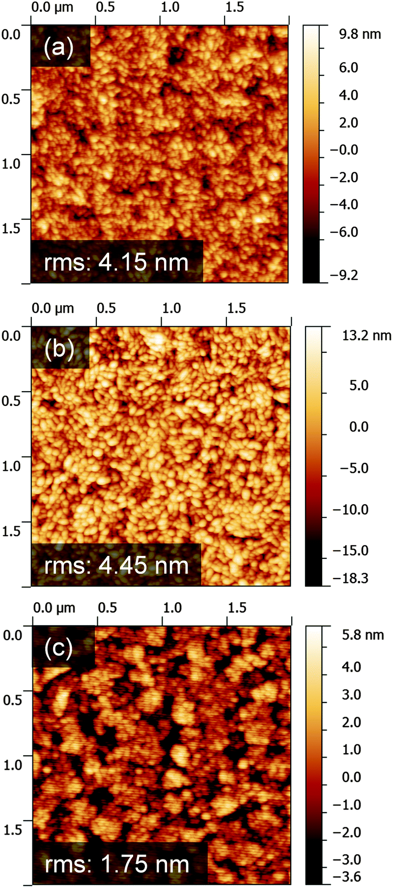 | ||
| Fig. 2 AFM topography images of 200 nm thick (a) ZnO and (b) Zn0.8Mg0.2O on ITO/glass substrates. (c) Topography of ITO/glass. | ||
We used electroabsorption spectroscopy (EA) to investigate whether the changes in operating voltage with Mg content were due to changes in the electron-injection barrier. With EA, we directly measure the change in the built-in potential (VBI) of the complete device as Mg content is varied. For this study, we used photoactive layers comprising 150 nm of poly(9,9-dioctylfluorene-alt-benzothiadiazole) (F8BT), rather than aryl-F8:0.5 wt% TFB, since F8BT has a well-defined electroabsorption response which lies in an accessible region of the visible spectrum. F8BT is also a less reactive material, allowing the long (∼1 h) integration times needed for data acquisition. A thin emitter was used to maximize the internal electric field necessary to observe a Stark shift in the F8BT absorption spectrum. However, since the emitter energy levels were fixed and only the electron-injector was changed, changes in the electron-injection barrier remain directly applicable to the blue PLEDs. Since the work function of the Zn1−xMgxO cathode lies within the F8BT bandgap, VBI represents the difference between the Zn1−xMgxO conduction band position and the MoO3 work function (Fig. 3a).35,36
 | ||
| Fig. 3 Measurement of the reduction in the electron-injection barrier using electroabsorption spectroscopy. (a) Illustration of the band-levels in an F8BT PLED obtained from ref. 28, 37 and 38, showing the electron-injection barrier and built-in potential (VBI). (b) Increase in the built-in potential of F8BT PLEDs with increasing Mg content in Zn1−xMgxO and the associated decrease in electron-injection barrier calculated using eqn (1). | ||
EA measurements were performed using a 525 nm monochromatic probe beam, corresponding to the strongest peak in the F8BT electroabsorption spectrum (Fig. 4a–d). The Stark shift was measured using a lock-in technique (see Experimental section), and tends to zero when a bias of VBI is applied to the electrodes. The electron-injection barrier (ΦB(cathode)) was calculated from eqn (1).
| ΦB(cathode) = Eg − qVBI − ΦB(anode) | (1) |
 | ||
| Fig. 4 Change in reflectance (dR) vs. photon energy (a–d) and applied bias (e and f) for ITO/(60 nm) Zn1−xMgxO/Cs2CO3/(150 nm) F8BT/(10 nm) MoO3/(50 nm) Au/(100 nm) Ag devices with (a and e) x = 0, (b and f) x = 0.2, (c and g) x = 0.44, (d and h) x = 0.6. The largest change in dR for (a–d) occurs at 2.36 eV (525 nm wavelength), which is the energy used to probe the bias response in (e–h). Built-in potentials were estimated from the voltage at which dR goes to zero. For x = 0, this was achieved by extrapolating from dR vs. V for negative bias, since under forward bias charges are injected which screen the internal field and change the electroabsorption spectrum. | ||
| Cathode | Cs2CO3 | V OC (V) | Bias at 200 cd m−2 (V) |
|---|---|---|---|
| ZnO | ✓ | 0.67 ± 0.09 (0.80) | 59 ± 7 (52) |
| ✗ | 0.71 ± 0.01 (0.72) | 84 ± 5 (80) | |
| Zn0.85Mg0.15O | ✓ | 0.8 ± 0.2 (1.1) | 55 ± 3 (52) |
| ✗ | 0.87 ± 0.07 (0.98) | 72 ± 3 (70) |
The role of the Cs2CO3 interlayer is indicated by measurements on hole-only F8BT devices (Fig. S9, ESI‡). These measurements show that the hole current density is reduced when the Cs2CO3 interlayer is present. Cs2CO3 may therefore act to reduce the movement of holes, reducing surface recombination, which is in agreement with a previous report.7 The improved charge carrier balance that results from this explains the lower operating voltages in the F8BT PLEDs with Cs2CO3 (Table 1). Cs2CO3 may play a similar role in our blue PLEDs, as suggested by Lu et al.8 The hole-only current densities of our blue PLEDs were unchanged with or without an interlayer, but this may be due to the hole current density being controlled by the TFB hole traps in the emitter, which prevent us from analyzing the boundary between the oxide and emitter.8 However, we found that the peak luminances of these blue PLEDs without Cs2CO3 interlayers fell below 1 cd m−2, regardless of whether the metal oxide was annealed (Fig. S10, ESI‡). This again suggests that the primary role of Cs2CO3 may be to prevent surface recombination of holes or of excitons in the metal oxide by limiting the movement of holes at the oxide-polymer boundary. PL quenching measurements (Fig. S11, ESI‡) were also in agreement with Cs2CO3 limiting hole injection into the oxide from the polymer. These measurements show that the PL intensity from aryl-F8:0.5 wt%TFB on Zn1−xMgxO was reduced by adding Cs2CO3 only when the oxide was unannealed. With Cs2CO3 limiting hole injection, electrons in the polymer can be injected into electron-acceptor states in the oxide,28 leading to exciton quenching. Annealing the oxide reduces the density of acceptor states, which could reduce the amount of exciton quenching. Thus, our hole-only, bipolar and PL measurements indicate that it is important to retain the Cs2CO3 interlayer in our devices to obtain high luminescent efficiency.
Despite the significant change in injection barrier achieved by tuning the Mg content, we found that when using 60 nm Zn1−xMgxO electrodes in aryl-F8:0.5 wt%TFB PLEDs, increasing x to more than 0.15 led to an increase in the average bias required to achieve a luminance of 1000 cd m−2, which we take as a characteristic operating point, rather than the expected decrease (Fig. 5a). We observed similar behavior in PLEDs based on F8BT (Fig. S12a, ESI‡). The likely cause of this reduced performance is an increase in the cathode resistivity for higher Mg contents in the Zn1−xMgxO, as shown in Table 2. To check this hypothesis and decouple the effects of energetics and resistivity, we used nitrogen-doped ZnO cathodes. Nitrogen is a p-type dopant for ZnO,39 which increases the oxide resistivity by decreasing the electron concentration, without changing the conduction band position.30,40 We found that as we increased the ZnO cathode resistivity through nitrogen doping, there was both a decrease in the luminous efficiency and an increase in the operating voltage (Table 3), precisely as observed for high Mg loading. For bulk Zn1−xMgxO electrodes, the potential benefit of the reduced electron-affinity is therefore masked by the concomitant increase in resistivity. To avoid the limitation of increased resistivity while still maintaining control over the interfacial electron injection level, we incorporated Mg only into the upper 10 nm of the metal oxide cathode (i.e. 10 nm Zn1−xMgxO on 50 nm ZnO). We found that the incorporation of Mg in only the top 10 nm of the cathode enabled a continuous reduction in operating voltage for Mg contents up to x = 0.44. This is a significant improvement over bulk Zn1−xMgxO, which only enabled a 1.5 V decrease in the average operating voltage for Mg contents up to x = 0.15. By contrast, using 10 nm Zn1−xMgxO on 50 nm ZnO as the cathode allowed the bias required to produce 1000 cd m−2 from our PLEDs to be reduced from 18 V to 15 V (Fig. 5b). This operating voltage is lower than that previously reported for aryl-F8:0.5 wt%TFB PLEDs of equivalent thickness on spray pyrolyzed ZnO.8 The trend in operating voltages was highly reproducible because the variation over several devices, shown by the error bars in Fig. 5a and b, were typically 3–5% of the average bias. The operating voltages do not reduce further for x > 0.44 due to the appearance of an insulating rocksalt MgZnO phase in the oxide, which significantly increased the voltage dropped across the cathode.28 Nevertheless, we found that incorporating Mg into the ZnO cathode does not reduce the lifetime of the PLEDs (Fig. S13, ESI‡).
 | ||
| Fig. 5 Applied bias required to produce 1000 cd m−2 luminance from aryl-F8:0.5 wt%TFB PLEDs on Zn1−xMgxO with Mg incorporated (a) into the bulk of the metal oxide films (i.e. 60 nm Zn1−xMgxO) and (b) into the top 10 nm of the metal oxide films (i.e. 50 nm ZnO/10 nm Zn1−xMgxO). The averages (dark points) and lowest biases measured (pale points) are shown. The dashed lines are to guide the eye. Current density–voltage curves of PLEDs with Mg incorporated into the (c) bulk and (d) surface of the cathode are shown right. To reduce the number of variable parameters, all films were annealed at 400 °C in air for 15 min and no pre-biasing was used. | ||
| Mg content (x) | 0 | 0.15 | 0.42 | 0.46 | 0.47 |
| Resistivity (Ω cm) | 0.04 | 0.18 | 0.21 | 6.0 | 11 |
| N doping (at%) | Resistivity (Ω cm) | Bias at 200 cd m−2 (V) | Bias at 2 mA cm−2 (V) | Peak luminous efficiency (cd A−1) | EQE (%) |
|---|---|---|---|---|---|
| 0 | 0.4 | 53 | 56 | 21 | 6.6 |
| 0.22 | 160 | 100 | 105 | 17 | 5.6 |
We note that variations between different device batches (e.g. the batches of polymer used and how long the blend had been mixed prior to use) also led to variations in operating voltage. For instance, the devices in Fig. 5a and c consistently exhibited operating voltages 2.5 V lower than those in Fig. 5b and d. However, comparisons of operating voltage can still be made within the same batch of devices, since they were processed under identical conditions, and are in all cases consistent with the description above. A reduction in operating voltage for both annealed and unannealed ZnO with surface Mg incorporation was also observed in the F8BT PLEDs (Fig. S15, ESI‡). In summary, we have shown in this section that reducing the electron-affinity of ZnO through Mg incorporation leads to a reduction in the operating voltages through a reduction in the electron-injection barrier. We also showed that incorporating Mg only to the surface of the cathode is advantageous over incorporating Mg into the entire bulk of the oxide because it allows the benefits of both the reduced electron-injection barrier and a low resistivity of the electrode.
Developing efficient, low-temperature processed blue PLEDs
Our findings have enabled us to produce efficient blue PLEDs with low operating voltages using processing temperatures ≤150 °C. A peak luminous efficiency of 6.5 cd A−1 (3.45% EQE) was obtained using an unannealed Zn0.85Mg0.15O electron-injector (Fig. 6), which was similar to the efficiency of the devices on Zn0.85Mg0.15O post-annealed at 400 °C for 15 min. These were both higher than the luminous efficiency of 5.9 cd A−1 (3.1% EQE) previously reported using spray pyrolyzed ZnO.8 Bulk rather than surface Mg incorporation was used in this case because the Mg content is sufficiently low that resistive effects are not dominant. Pre-biasing the PLEDs on unannealed Zn0.85Mg0.15O at 10 V for 1 s allowed us to overcome the low emission obtained at applied biases below 20 V, such that the luminous efficiency and luminance curves became almost identical to those of PLEDs on annealed Zn0.85Mg0.15O (Fig. 6). PLEDs on the unannealed oxide also produced the same electroluminescence spectrum as those on the annealed oxide (Fig. S16, ESI‡). Through a combination of pre-biasing and reduction of the electron-injection barrier by incorporating Mg into unannealed ZnO, the bias required to produce 1000 cd m−2 was reduced to 14 V, 26% lower than that required from aryl-F8:0.5 wt% TFB PLEDs of the same thickness (450 nm) on ZnO deposited by spray pyrolysis at 400 °C.8 Fourteen pre-biased blue PLEDs on unannealed Zn0.85Mg0.15O were measured, yielding an uncertainty of ± 0.3 V in the operating voltage, showing that this system was highly reproducible. The maximum luminance measured from these PLEDs was 24000 cd m−2 after pre-biasing (compared to 12000 cd m−2 achievable using annealed AP-CVD Zn0.85Mg0.15O). This is three times larger than previously reported using spray pyrolyzed ZnO grown at 400 °C.8 The architecture and device processing method that we have developed to achieve record performances from blue PLEDs can be applied directly to newly developed emissive layers. These include LEDs using phosphorescence or thermally activated delayed fluorescence41 to increase efficiencies further by harvesting triplet excitons.
 | ||
| Fig. 6 Luminous efficiency (closed symbols and solid lines) and luminance (open symbols and dotted lines) vs. applied bias for aryl-F8:0.5 wt%TFB PLEDs on Zn0.85Mg0.15O. A comparison is made between PLEDs on Zn0.85Mg0.15O annealed at 400 °C for 15 min in air, unannealed Zn0.85Mg0.15O and unannealed Zn0.85Mg0.15O but biased at 10 V for 1 s prior to measuring (pre-biased). | ||
Having developed our cathode structure with thick emitter PLEDs, which are simpler to study and easier to produce industrially,4 we applied our findings to thin PLEDs. The operating voltages of PLEDs proportionally decrease with the emitter thickness.4 We found that using our optimized structure in a PLED with an 80 nm thick emitter led to a turn-on voltage of only 3.7 V (Fig. S17, ESI‡). This is comparable to industry-standard inorganic blue LEDs,42 although our polymer LEDs have the important advantage of roll-to-roll processing compatibility.1
Conclusions
In conclusion, we have shown that high efficiency, low operating voltage blue aryl-F8:0.5 wt%TFB PLEDs can be produced with oxide cathodes processed at temperatures 250 °C lower than previously used. Pre-biasing the PLEDs at 10 V for 1 s prior to measurements allowed us to increase the performance of PLEDs based on unannealed oxide cathodes to approach the performance of PLEDs based on annealed oxides. Operating voltages were further reduced by lowering the barrier to electron-injection, as measured by electroabsorption spectroscopy. A record luminance of 24000 cd m−2 was achieved from our blue PLEDs with a higher luminous efficiency (6.5 cd A−1 compared to 5.9 cd A−1) using unannealed Zn0.85Mg0.15O synthesized atmospherically at 150 °C. The operating voltages were also 26% lower than previously reported for nominally identical PLEDs using spray pyrolyzed ZnO processed at 400 °C. We also established that Cs2CO3 interlayers enable higher luminescent efficiencies by preventing surface recombination in the oxide. Our findings are a crucial step towards low-cost, large area flexible displays and lighting reliant on efficient PLEDs of the three primary colors.
Experimental
Bipolar polymer light emitting diode fabrication
We synthesized our films using an AP-SALD reactor operating in CVD conditions due to a large substrate-manifold spacing. A detailed explanation of this can be found in ref. 21. These AP-CVD films were deposited at 150 °C according to previous reports on ITO/glass (Colorado Concepts LLC), ultrasonically cleaned in toluene and isopropanol.21,28 The films were both used as-deposited and annealed at 400 °C for 15 min in air. When the interlayer of Cs2CO3 (5 mg mL−1; 2-methoxyethanol) was used, it was spin-cast on the metal oxide films at 6000 rpm for 45 s. Aryl-F8 (30 mg mL−1; p-xylene) had 0.5 wt% TFB mixed into it. The resulting aryl-F8:0.5 wt%TFB was spin-cast at 2000 rpm for 45 s over the Cs2CO3, giving a 450 nm thick film. This was annealed in a nitrogen-filled glovebox at 120 °C for 1 h. For thin yellow-green PLEDs, F8BT (20 mg mL−1; p-xylene) was spin-cast on Cs2CO3 at 2000 rpm for 45 s, giving a 150 nm layer. For thick yellow-green PLEDs, F8BT (45 mg mL−1; p-xylene) was spin-cast at 2000 rpm for 45 s, giving a 1000 nm layer. Both types of F8BT devices were annealed in a nitrogen-filled glovebox at 160 °C for 1 h. TFB (20 mg mL−1) was spin-cast at 700 rpm for 45 s on the annealed F8BT, giving a 200–240 nm thick TFB layer to reduce hole current flow. For all three types of PLEDs, 10 nm MoO3 and 50 nm Au were thermally evaporated through a shadow mask, giving 5.25 mm2 pixels. The thin F8BT PLEDs used in electroabsorption measurements did not have a TFB layer on top to avoid signal convolution and also had 100 nm Ag evaporated over the MoO3/Au to increase the reflection of the monochromatic light signal.Single-carrier device fabrication
Electron-only devices were made in an almost identical structure to the bipolar devices. The only difference was that the top electrode consisted of 20 nm Ca, covered with 100 nm Ag. For the hole-only devices, PEDOT:PSS (Clevios) was spin-cast at 6000 rpm for 30 s on ITO/glass (Colorado Concepts LLC; cleaned ultrasonically in acetone and isopropanol and 10 min oxygen plasma), followed by annealing in air at 180 °C for 20 min. The Cs2CO3, polymer emitter, TFB, MoO3 and Au were deposited over this in the same way as bipolar PLEDs.Device and film characterization
A silicon photodiode and Keithley 2400 source measure unit were used to measure the luminous efficiency, luminance, external quantum efficiency and current density from the devices. A Labsphere CDS-610 spectrometer was used to measure the electroluminescence spectra. Electroabsorption spectroscopy was performed using two light sources: a 150 W xenon arc lamp (Oriel 6253) and 50 W quartz tungsten halogen lamp (Oriel 6332). These were passed through a monochromator (Newport 7340) so that specific wavelengths could be selected (525 nm was used for the D.C. bias sweeps). The devices were positioned so that the incident monochromatic beam was reflected onto a silicon photodiode (OPT 301). The voltage signal had a D.C. component that was swept from −3 V to +3 V with an A.C. component that had an amplitude of 0.5 VRMS and frequency of 5.16 kHz. To detect the change in reflectance due to the applied bias, a dual channel lock-in amplifier was used (SR 830; Stanford Research Systems). Photoluminescence measurements on Zn1−xMgxO were performed using an Accent RPM 200 system using a Nd:YAG laser (4.5 mW power, 266 nm wavelength). The film resistivity was measured in the Van der Pauw configuration using a previously-reported technique.28 Atomic force microscopy (AFM) images were obtained using a Veeco dimension 3100, operated in tapping mode and using a Si tip (MikroMasch, 325 kHz resonant frequency). Open-circuit voltage measurements were performed under AM 1.5G 1-sun illumination using a previously reported method.28 Ultraviolet photoelectron spectroscopy (UPS) was performed using an Omicron ultrahigh vacuum system with 21.22 eV illumination from a He(I) emission line according to a previous report.43 The substrates were silicon with Cr/Au thermally evaporated onto them. Zn1−xMgxO was deposited with a thickness of ∼15 nm onto the conductive gold layer, with was grounded during measurements.Acknowledgements
The authors gratefully thank the help of Patrick R. Brown and Prof. Vladimir Bulović for performing UPS measurements, and Abhijeet Sangle for assistance with X-ray diffraction measurements. The authors would also like to acknowledge funding from the Cambridge Commonwealth, European and International Trusts, the Rutherford Foundation of New Zealand, Girton College Cambridge, A*STAR National Science Scholarship (Republic of Singapore), Indo-UK APEX project, ERC Advanced Investigator Grant, Novox, ERC-2009-adG247276, EPSRC (Reference: EP/G060738/1), Cambridge Display Technology and the Royal Society.Notes and references
- J. H. Burroughes, D. D. C. Bradley, A. R. Brown, R. N. Marks, K. Mackay, R. H. Friend, P. L. Burns and A. B. Holmes, Nature, 1990, 347, 539–541 CrossRef CAS PubMed.
- M. T. Bernius, M. Inbasekaran, J. O’Brien and W. Wu, Adv. Mater., 2000, 12, 1737–1750 CrossRef CAS.
- S. Reineke, F. Lindner, G. Schwartz, N. Seidler, K. Walzer, B. Lüssem and K. Leo, Nature, 2009, 459, 234–239 CrossRef CAS PubMed.
- D. Kabra, L. P. Lu, M. H. Song, H. J. Snaith and R. H. Friend, Adv. Mater., 2010, 22, 3194–3198 CrossRef CAS PubMed.
- Y. Shimada, J. Ishino, S. Shirasaki, T. Irie and A. Kikuchi, Displays, 2013, 34, 437–441 CrossRef CAS PubMed.
- J. Bharathan and Y. Yang, Appl. Phys. Lett., 1998, 72, 2660 CrossRef CAS PubMed.
- L. P. Lu, D. Kabra and R. H. Friend, Adv. Funct. Mater., 2012, 22, 4165–4171 CrossRef CAS PubMed.
- L.-P. Lu, D. Kabra, K. Johnson and R. H. Friend, Adv. Funct. Mater., 2012, 22, 144–150 CrossRef CAS PubMed.
- B. R. Lee, W. Lee, T. L. Nguyen, J. S. Park, J. Kim, J. Y. Kim, H. Y. Woo and M. H. Song, ACS Appl. Mater. Interfaces, 2013, 5, 5690–5695 CAS.
- R. L. Z. Hoye, D. Muñoz-Rojas, D. C. Iza, K. P. Musselman and J. L. MacManus-Driscoll, Sol. Energy Mater. Sol. Cells, 2013, 116, 197–202 CrossRef CAS PubMed.
- B. R. Lee, E. D. Jung, J. S. Park, Y. S. Nam, S. H. Min, B.-S. Kim, K.-M. Lee, J.-R. Jeong, R. H. Friend, J.-S. Kim, S. O. Kim and M. H. Song, Nat. Commun., 2014, 5, 4840 CrossRef CAS PubMed.
- J. H. Cook, J. Santos, H. Li, H. A. Al-Attar, M. R. Bryce and A. P. Monkman, J. Mater. Chem. C, 2014, 2, 5587–5592 RSC.
- R. L. Z. Hoye, M. R. Chua, K. P. Musselman, G. Li, M.-L. Lai, Z.-K. Tan, N. C. Greenham, J. L. MacManus-Driscoll, R. H. Friend and D. Credgington, Adv. Mater., 2015, 27, 1414–1419 CrossRef CAS PubMed.
- M. C. Gwinner, D. Kabra, M. Roberts, T. J. K. Brenner, B. H. Wallikewitz, C. R. McNeill, R. H. Friend and H. Sirringhaus, Adv. Mater., 2012, 24, 2728–2734 CrossRef CAS PubMed.
- L.-M. Chen, Z. Xu, Z. Hong and Y. Yang, J. Mater. Chem., 2010, 20, 2575–2598 RSC.
- Y. Vaynzof, D. Kabra, L. L. Chua and R. H. Friend, Appl. Phys. Lett., 2011, 98, 113306 CrossRef PubMed.
- H. J. Bolink, E. Coronado, J. Orozco and M. Sessolo, Adv. Mater., 2009, 21, 79–82 CrossRef CAS PubMed.
- M.-H. Park, J.-H. Li, A. Kumar, G. Li and Y. Yang, Adv. Funct. Mater., 2009, 19, 1241–1246 CrossRef CAS PubMed.
- T.-W. Lee, J. Hwang and S.-Y. Min, ChemSusChem, 2010, 3, 1021–1023 CrossRef CAS PubMed.
- Y.-H. Kim, T.-H. Han, H. Cho, S.-Y. Min, C.-L. Lee and T.-W. Lee, Adv. Funct. Mater., 2014, 24, 3808–3814 CrossRef CAS PubMed.
- R. L. Z. Hoye, D. Muñoz-Rojas, K. P. Musselman, Y. Vaynzof and J. L. MacManus-Driscoll, ACS Appl. Mater. Interfaces, 2015, 7, 10684–10694 CAS.
- D. C. Iza, D. Muñoz-Rojas, Q. Jia, B. Swartzentruber and J. L. Macmanus-Driscoll, Nanoscale Res. Lett., 2012, 7, 655 CrossRef PubMed.
- Y. Yang, P. Cohn, S.-H. Eom, K. A. Abboud, R. K. Castellano and J. Xue, J. Mater. Chem. C, 2013, 1, 2867–2874 RSC.
- U. Giovanella, C. Botta, F. Galeotti, B. Vercelli, S. Battiato and M. Pasini, J. Mater. Chem. C, 2013, 1, 5322 RSC . In this reference, a maximum EQE of 5.02% is reported, but the corresponding luminous efficiency is only 1.07 cd A−1, which, unexpectedly, is lower than the luminous efficiency of a 2.7% EQE PLED with comparable CIE coordinates in ref. 12.
- J. F. Cordaro, Y. Shim and J. E. May, J. Appl. Phys., 1986, 60, 4186 CrossRef CAS PubMed.
- G. Chicot, P. Muret, J.-L. Santailler, G. Feuillet and J. Pernot, J. Phys. D: Appl. Phys., 2014, 47, 465103 CrossRef.
- J. Dane and J. Gao, Appl. Phys. Lett., 2004, 85, 3905 CrossRef CAS PubMed.
- R. L. Z. Hoye, B. Ehrler, M. L. Böhm, D. Muñoz-Rojas, R. M. Altamimi, A. Y. Alyamani, Y. Vaynzof, A. Sadhanala, G. Ercolano, N. C. Greenham, R. H. Friend, J. L. MacManus-Driscoll and K. P. Musselman, Adv. Energy Mater., 2014, 4, 1301544 Search PubMed.
- M. Lu, P. De Bruyn, H. T. Nicolai, G.-J. A. H. Wetzelaer and P. W. M. Blom, Org. Electron., 2012, 13, 1693–1699 CrossRef CAS PubMed.
- K. P. Musselman, S. Albert-Seifried, R. L. Z. Hoye, A. Sadhanala, D. Muñoz-Rojas, J. L. MacManus-Driscoll and R. H. Friend, Adv. Funct. Mater., 2014, 24, 3562–3570 CrossRef CAS PubMed.
- I.-T. Cho, J.-M. Lee, J.-H. Lee and H.-I. Kwon, Semicond. Sci. Technol., 2009, 24, 015013 CrossRef.
- R. L. Z. Hoye, S. Heffernan, Y. Ievskaya, A. Sadhanala, A. J. Flewitt, R. H. Friend, J. L. MacManus-Driscoll and K. P. Musselman, ACS Appl. Mater. Interfaces, 2014, 6, 22192–22198 CAS.
- T. J. Whitcher, K. H. Yeoh, Y. B. C. Ng, N. A. Talik, C. L. Chua, K. L. Woon, N. Chanlek, H. Nakajima, T. Saisopa, P. Songsiriritthigul, S. Oswald and B. K. Yap, J. Phys. D: Appl. Phys., 2013, 46, 475102 CrossRef.
- Y.-J. Choi, S. C. Gong, K.-M. Kang and H.-H. Park, J. Mater. Chem. C, 2014, 2, 8344–8349 RSC.
- D. C. Olson, S. E. Shaheen, M. S. White, W. J. Mitchell, M. F. A. M. van Hest, R. T. Collins and D. S. Ginley, Adv. Funct. Mater., 2007, 17, 264–269 CrossRef CAS PubMed.
- T. M. Brown, R. H. Friend, I. S. Millard, D. J. Lacey, T. Butler, J. H. Burroughes and F. Cacialli, J. Appl. Phys., 2003, 93, 6159 CrossRef CAS PubMed.
- A. Kumar, G. Pace, A. A. Bakulin, J. Fang, P. K. H. Ho, W. T. S. Huck, R. H. Friend and N. C. Greenham, Energy Environ. Sci., 2013, 6, 1589 CAS.
- H. J. Bolink, E. Coronado, D. Repetto and M. Sessolo, Proc. SPIE, 2008, 6999, 69992X CrossRef PubMed.
- L. Dunlop, A. Kursumovic and J. L. MacManus-Driscoll, Appl. Phys. Lett., 2008, 93, 172111 CrossRef PubMed.
- B. Ehrler, K. P. Musselman, M. L. Böhm, F. S. F. Morgenstern, Y. Vaynzof, B. J. Walker, J. L. MacManus-Driscoll and N. C. Greenham, ACS Nano, 2013, 7, 4210–4220 CrossRef CAS PubMed.
- Q. Zhang, B. Li, S. Huang, H. Nomura, H. Tanaka and C. Adachi, Nat. Photonics, 2014, 8, 326–332 CrossRef CAS PubMed.
- Y. Liu, C. Huang, T. Chen, C. Hsu, S. Cheng, K. Lin, J. Liou and W. Liu, Prog. Nat. Sci., 2010, 20, 70–75 CrossRef.
- P. R. Brown, D. Kim, R. R. Lunt, N. Zhao, M. G. Bawendi, J. C. Grossman and V. Bulović, ACS Nano, 2014, 8, 5863–5872 CrossRef CAS PubMed.
Footnotes |
| † The dataset for this study may be accessed at http://www.repository.cam.ac.uk/handle/1810/250291. |
| ‡ Electronic supplementary information (ESI) available: Supporting optical, electrical, X-ray diffraction, ultraviolet photoelectron spectroscopy and electroluminescence measurements available. See DOI: 10.1039/c5tc01581b |
| This journal is © The Royal Society of Chemistry 2015 |