
 Open Access Article
 This Open Access Article is licensed under a Creative Commons Attribution-Non Commercial 3.0 Unported Licence
Precursor strategies for metallic nano- and micropatterns using soft lithography†
F. M.
Wisser
a,
B.
Schumm
b,
G.
Mondin
a,
J.
Grothe
*a and
S.
Kaskel
ab
aDresden University of Technology, Bergstrasse 66, 01069 Dresden, Germany. E-mail: julia.grothe@chemie.tu-dresden.de; Fax: +49 351 463 37287; Tel: +49 351 463 33632
bChemical Surface and Reaction Technology Department, Fraunhofer Institute for Material and Beam Technology IWS, Winterbergstraße 28, 01277 Dresden, Germany
First published on 13th February 2015
Abstract
Soft lithographic methods describe a set of printing methods which are widely used for the preparation of structured surfaces. Structured surfaces are essential components in the field of (opto-)electronic devices such as organic light emitting diodes, photovoltaics or organic field effect transistors. In recent years, crucial progress has been achieved in the development of patterned metal coatings for these applications. This review focusses on new strategies for soft lithographical printing of metal structures emphasizing the subtle interplay of printing techniques, metal precursor chemistry, and surface functionalization strategies.
 F. M. Wisser | Florian M. Wisser studied chemistry at the Saarland University and at the European School of Chemistry, Polymers and Materials Science (ECPM) in Strasbourg. In 2011 he received diploma degrees from both universities. Since 2011, he has been pursuing a PhD thesis in the group of Prof. Kaskel at Dresden University of Technology. His interests are micro- and nanostructured materials for sensing applications and their preparation by soft lithographic methods. |
 B. Schumm | Benjamin Schumm studied chemistry at Dresden University of Technology from where he received his Diploma degree in 2009. He joined the group of Prof. Kaskel as a PhD student, where his main research interests were in the field of precursor synthesis for nanoimprinting transparent contacts in optoelectronic devices. Since 2013, he is research associate at Fraunhofer Institute IWS in Dresden. |
 G. Mondin | Giovanni Mondin received his BS in 2008 and his MS in 2011 in materials science from University of Padua, Italy. He is currently pursuing his PhD degree in inorganic chemistry at Dresden University of Technology under the direction of Prof. Stefan Kaskel. His research topics include soft lithography, electroless plating and nanotechnology. |
 J. Grothe | Julia Grothe studied chemistry at the University of Regensburg and received her diploma degree in 2003. Under the direction of Prof. Kaskel she received her PhD in inorganic chemistry from Dresden University of Technology in 2008. In 2009 she returned to the inorganic chemistry department as a group leader for nanomaterials. Her current research interests include nanocomposite materials and nanostructured thin films. |
 S. Kaskel | Stefan Kaskel received his PhD in Inorganic Chemistry from Tübingen University in 1997. He was a Postdoctoral Humboldt-Fellow with Professor J. D. Corbett at the Ames Lab (USA). In 2000 he joined the MPI for Coal Research (Mühlheim a.d. Ruhr), as a group leader. Since 2004 he has been a full Professor in Inorganic Chemistry at the Dresden University of Technology and 2008 he was co-appointed at the Fraunhofer Institute for Material and Beam Technology as head of the CVD and thin film department. His research interests include synthesis and characterization of porous and nanostructured materials. |
Introduction
Metallic nano- and microstructures are essential in numerous applications, especially in the fields of microelectronics, opto-electronics, and plasmonics. The conventional methods to manufacture metal nano- and microstructures are based on photolithography to pattern a resist in combination with a metal deposition method such as physical vapor deposition (e.g. sputtering, arc deposition, vacuum evaporation), electroplating, electroless plating or, to a lesser extent, chemical vapor deposition.1 Other scientific methods for the preparation of structured templates prior to metal deposition are based on the self assembly of inorganic nano particles or block-co-polymers.1,2 In the early 90s of the last century soft lithography was pioneered by Whitesides as an alternative metal patterning approach for microelectronics applications.3–5 Soft lithography is a set of methods based on the use of an elastomeric stamp and was developed to circumvent the limitations of photolithography, in particular its complexity, low through-put and costs due to necessary sophisticated equipment.6 Soft lithography is very well suited for an extensive range of applications where uniformity and alignment of the metal features are not major concerns, for instance the fabrication of transparent electrodes for photovoltaic applications, sensors, metal etching masks, and wiring of printed circuits.7This review describes the different approaches based on soft lithography used to fabricate metallic nano- and microstructures. Metallic patterns can be fabricated using both top-down and bottom-up methods. This review is mainly focused on bottom-up approaches (precursor chemistry) as they have received more and more attention since the second half of the 2000s: this is due to the fact that they do not involve an etching step as compared to top-down strategies and are therefore less time-consuming and more environmental friendly. Also they involve less material loss, a crucial aspect to improve resource efficiency. However, the top-down approaches based on the selective etching of a metal layer are also briefly reviewed given their great influence in the soft lithography field.
Patterning techniques
Direct printing methods
Inkjet printing technology goes back to the nineteenth century and has developed to be the most widely used printing technique in publishing industry but also in personal households in the last century. Being a “direct writing technique” without any needs for masks it is attractive due to low costs, low material waste and flexible production conditions. A plethora of publications have been released in the last decade on the use of the technique for printing of organic electronics, circuit components, radio-frequency identification tags, solar cells, displays, electrical interconnects and other applications.8–10 New inkjet printers usually work with piezoelectric drop-on-demand printheads. The printheads are filled with the ink and sequences of droplets are ejected through a nozzle on demand. When voltage is applied to the piezoelectric actuator, pressure waves form as a result of a sudden volume change. Droplets are ejected when a positive pressure wave approaches the nozzle.11 The whole printing process consists of drop ejection, drop flight, drop impact on the substrate, drop spreading and solidification.12 The understanding of all five stages is essential for high quality and high resolution printing and intensive investigations have been carried out on each single step of the process.13–15 However even under optimum conditions the resolution of drop-on-demand inkjet printing is limited to few tens of micrometers due to the minimum nozzle diameters and broadening of the ink on the substrate.11,16 Also a phenomenon usually called “coffee staining” has been described several times when the solvent of the ink evaporates from the edges and less or even no material remains in the centre.17 However the “coffee staining” effect can be decreased by heating the substrate before printing and use of highly concentrated inks with lower viscosities.18 In order to obtain higher resolutions new techniques have been developed such as electrodynamic jet printing, laser processing or dip-pen-like dragging.19Soft lithography methods
Today, the most common patterning techniques for micro- and nanostructuring of various surfaces are based on hard lithography techniques. These methods mainly use e-beam, X-ray, ultraviolet or visible light for patterning a photoresist either through a mask or directly by scanning techniques. The partial removal of the resist allows etching and thus patterning of the substrate. The main disadvantage of these techniques is related to the high costs for the equipment.To overcome this disadvantage, Whitesides et al. developed new non-photolithographic micropatterning techniques for surface modification on the micro- and even nanoscale using flexible molds or stamps in the 1990s.4 These methods allow low-cost patterning for laboratory use by using a previously patterned stamp instead of “hard” radiation (UV/Vis, X-ray or e-beam) and are thus called “soft lithography” techniques. Elastomers like polydimethylsiloxane (PDMS) are often used as flexible material for the stamp preparation, giving another hint for this denomination. Besides pure stamping methods, also masking and molding processes were developed. All the techniques are fast, simple and cheap tools for lab-scale micro- and nanostructuring of surfaces. But also large and non-planar (rough or curved) areas can be treated with a variety of “ink” materials.7Fig. 1 summarizes frequently used soft lithography techniques and principles. Among them, the earliest developed method, microcontact printing, represents a form of contact printing that uses a high-resolution elastomeric stamp where the surface is covered with a chemical ink capable of forming a self-assembled monolayer. Whitesides et al. used these kinds of patterned monolayers to achieve a patterned material deposition on the substrate. Often bifunctional thiols are stamp-printed on gold surfaces where a monolayer is created via thiol bonding. The other functional group acts as an anchor for subsequent functionalization with other substances or particles. Another field of application for microcontact printing can be seen in the partial protection of the surface by the monolayer. In this case the deposited molecules prevent the surface of being attacked by etchants or similar substances. Without expensive facilities, microcontact printing offered the first way to form various high-resolution patterns (<100 nm) using standard laboratory equipment.
 | ||
| Fig. 1 Illustration of frequently used soft lithography techniques: microcontact printing, UV or thermal NIL, soft embossing NIL or SANIL and micromolding in capillaries. | ||
The advantages of microcontact printing have been adapted to replica molding as it has been used for the mass-production of a wide range of structured surfaces such as compact disks (CDs), diffraction gratings or holograms.20–22 While these techniques are based on molding against a rigid mold with an appropriate material (usually a thermoplastic polymer), the use of elastomers makes it easier to release small, fragile structures. Consequently, nanoimprint lithography (NIL) was developed allowing the surface patterning with feature heights up to a few micrometers. Chou et al. originally introduced NIL as a process where a rigid stamp is pressed into a PMMA layer on a rigid silicon substrate under slight thermal treatment.23 By this method an appropriate alternative for photolithographic resist patterning could be achieved with resolutions in the range of some ten nanometers.24 Today, the term NIL is used in a broader view. It describes the process of patterning a polymer layer by pressing a stamp – rigid or flexible – in a pre-polymer layer coated on a substrate. As pre-polymer various substances such as monomers, oligomers, polymers or solutions thereof can be used. After e.g. UV or thermal curing of the pre-polymer and stamp removal a patterned coating is formed.
With the step-and-flash imprint lithography (S-FIL) the imprint process was extended by Colburn et al. to solutions of curable substances.25 This allows the patterning directly after deposition of pre-polymer droplets – a uniform pre-polymer layer is not required. In further developments called soft embossing NIL or solvent assisted NIL (SANIL) the method could be extended to a broad range of materials. Embossing in polymer solutions or even sol–gel precursors were applied in the NIL-process.26,27 Thus, nanostructured high-quality inorganic films can be prepared by patterning a polymer containing a high ratio of inorganic material and subsequent burning of the organic matrix.28 To avoid an undesired residual layer between the features, a technique called micromolding in capillaries (MIMIC) or capillary force lithography was developed.29 Here the stamp is pressed against the uncoated substrate exposing channels or capillaries to at least one side. A low-viscosity precursor or polymer solution is subsequently placed in front of the channels. Due to capillary forces enhanced by solvent evaporation through the stamp material, the solution is soaked into the channels. Complete solvent evaporation leads to patterns of the precursor or polymer only in the areas where the channels were formed.
In order to accelerate the flowing of the fluid in the channels, Tvingstedt et al. developed in 2007 a method in which air is extracted with a syringe from one side of the channels between the patterned stamp and the pre-activated substrate, speeding up the capillary flow of the ink solution from the other side of the stamp (Fig. 2).30 However the methods requires interconnected cavities in order to allow complete infiltration.
 | ||
| Fig. 2 (A) drawing of the MIMIC-based experimental set-up by Inganäs et al., showing on the left the syringe used to extract air from the channels of a PDMS stamp placed on a substrate, generating a low pressure which accelerates the capillary flow of the electroless silver solution from the right side. (B) Optical microscope image of the silver structures fabricated as shown in (A). The scale bar is 1 mm. Reprinted with permission from ref. 30. Copyright (2007) Wiley. | ||
The simple and cheap stamp preparation and handling allowed the development of a pool of soft lithography processes all based on the application of an elastomeric stamp or mold as a patterning tool. These include microfluidic approaches, combined optical/soft lithography methods and many more.7
Stamp materials used for soft lithography
As described above, initially rigid stamp materials were used for NIL and related techniques. Patterned silicon, silicon oxide or metals found application. In NIL processes with these materials as molds feature resolutions below 10 nm have been realized.31 In case of lower restrictions in terms of resolution and aspect ratio, PDMS is a suitable mold material for NIL as well. As this elastomer can be wound around cylinders, it allows large area and high throughput processing by integration in efficient roll-to-roll processes.32,33The flexible PDMS stamp is prepared by casting a blend of silicone oligomers with a cross-linker and a catalyst on a perfluorinated silicon “master”-mold (Fig. 3). The master has to be fabricated using microlithographic methods and can be reused. After thermal cross-linking, the elastomeric stamp can be peeled off and used for patterning as it is.34 Besides silicon, also other structured materials such as polymers or metals can also be considered as molds for PDMS stamp fabrication.
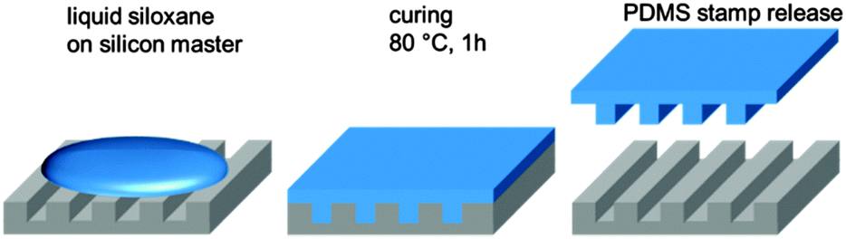 | ||
| Fig. 3 Scheme of the PDMS stamp preparation process. The siloxane oligomer liquid is poured onto a patterned silicon wafer. After thermal cross-linking, the flexible replica can be peeled off. | ||
Polydimethylsiloxanes are ideal featuring a unique combination of properties resulting from the presence of a siloxane backbone and organic methyl groups attached to silicon atoms.35 In addition to its elasticity, the low interfacial surface energy is a useful property for soft lithography applications as it leads to low adhesion, little chemical interaction and no swelling by humidity. Furthermore, gases and evaporated organic solvents pass the PDMS membrane easily, enabling solvent-assisted patterning. With its good thermal stability (up to approx. 180 °C in air) PDMS enables thermal molding or imprinting of various materials. Additionally, an optical transparency down to ∼300 nm allows UV-curing of pre-polymers through the PDMS membrane. Oligomeric siloxanes are fluids at room temperature and can be readily converted into solid elastomers by cross-linking. For a broad range of soft lithographic applications the stamp preparation is carried out by crosslinking of methylhydrosiloxane oligomer with a vinyl terminated dimethylsiloxane oligomer in a catalytic hydrosilylation using a platinum based catalyst (Fig. 4). Commercial kits for PDMS fabrication are available in large quantities from several companies (e.g. Dow Corning Sylgard 184).
 | ||
| Fig. 4 Chemical structure of methylhydrosiloxane oligomer and cross linker for the H2PtCl6-catalysed hydrosilylation towards flexible PDMS. | ||
Generally, PDMS is a satisfying mold material for many nanofabrication processes involving features on the order of ∼500 nm. However, there are some inherent disadvantages with this material that have to be overcome if a sub-100 nm resolution is required. The low modulus of elasticity of 2.0 MPa limits the feature size and aspect ratio that can be replicated.36 In addition, PDMS swells when exposed to some common organic solvents and the fact that Sylgard 184 needs to be thermally cured limits the numbers of materials useable as master-mold.37
To overcome these disadvantages, high-modulus and photocurable h-PDMS (9 MPa36) as well as thiolene (poly[(3-mercaptopropyl)-methylsiloxane] (PMMS), 41 MPa38) acrylate based molds have been developed.38,39 Higher resolutions and aspect ratios could be realized as compared to Sylgard 184.
There are plenty of other stamp materials available all suitable for specific applications. Here we address especially materials for high-resolution patterning.
Williams et al. have introduced perfluoropolyether-based (PFPE) elastomers that offer high modulus (155 MPa), low surface energy, solvent resistance, chemical stability and high visible light transparency. This flexible material allows a resolution down to 20 nm with high aspect ratios and opens the door for the soft lithography based preparation of three-dimensional nanostructured microobjects.40 Even higher elastic modulus stamp materials were realized allowing large area high aspect ratio patterning with ∼15 nm resolution. These relatively rigid materials (e.g., ETFE – ethylene(tetrafluoroethylene)) with an elastic modulus of ∼1 GPa, or PUA – polyurethane-acrylate based materials with an elastic modulus of 2.7 GPa are especially suited for high-resolution thermal imprinting.41,42 However, all of these stamp materials cannot compete with PDMS in terms of price or processability for sub-micrometer patterning.
Metallic nano- and micropatterns via top-down approach
Metallic patterns can be fabricated using a top-down strategy by selectively removing metal sections from a metal coating on a substrate surface. This is usually done by selectively etching the metal layer, while a patterned etching resist protects the desired metal regions. In this way, any planar metal pattern can be fabricated. In this chapter the top-down approaches based on etching and soft lithography used to fabricate metallic patterns are described. Soft lithography is used in this case to selectively pattern the etching resist. This approach was introduced by the Whitesides group and extensively investigated in the nineties of the last century and in the first years of the 2000s as an alternative to the standard photolithography process used to pattern etching resists.3–5 The original top-down approach from the Whitesides group to pattern metal films is based on the use of self-assembled monolayers (SAM) to selectively block the etching process and was published in 1992,3 followed the year after by the famous paper in which for the first time microcontact printing was used to print a solution of alkanethiol to form SAMs on a gold substrate with a patterned PDMS stamp.4 The substrate was then immersed in an aqueous solution of potassium cyanide (1 M KOH, 0.1 M KCN) to selectively etch the exposed gold regions. The authors fabricated gold features with sizes in the micrometer up to the centimeter range. In the following years, Whitesides et al. also applied this approach to the selective etching of silver, copper, aluminum and the fabrication of metallic submicrometer structures on curved surfaces.43–46 Particularly interesting is the fabrication of 3D metallic structures (“microorigami”), starting from planar features fabricated with the selective etching approach, followed by the folding of such features and their consolidation by electroplating.47,48In the early 2000s the IBM Zurich Research Laboratory significantly contributed to the improvement of the top-down approach based on soft lithography for the fabrication of metal patterns.49,50 In particular, they introduced the use of flat PDMS stamps, instead of patterned PDMS stamps, which are inked by pressing them against a patterned inker pad.49 As in the standard microcontact printing process, the flat stamp is then pressed against a substrate, transferring the ink. The use of flat stamps ensures the advantages of a patterned stamp, but in addition eliminates the mechanical drawbacks associated with small elastomeric features, such as buckling and roof collapse.7,49 The same authors developed also the positive microcontact printing approach.50 In this method the printed areas of the substrate are etched instead of being protected. In the original work, this is achieved by printing pentaerythritol-tetrakis(3-mercaptopropionate) (PTMP) on a metal substrate, followed by the immersion of the substrate on a solution containing eicosanethiol (ECT), which are adsorbed only on the PTMP-free areas. The substrate is then etched with a solution that selectively etches only the areas printed with PTMP, while the ECT prevents the etching. The authors fabricated several gold and copper structures with sizes in the micrometer range. The positive microcontact printing method was later also used by other groups.51,52
In 2009 and 2010 the Huskens group used a flat stamp approach to achieve sub-100 nm gold structures, using nanoimprint lithography and capillary force lithography, respectively, to selectively ink the flat PDMS stamp.53,54 Particularly interesting is a new top-down approach based on subtractive patterning via chemical lift-off lithography and introduced in 2012 by Liao et al.55 In this method a PDMS stamp activated by oxygen plasma is used to remove hydroxyl-terminated SAMs from gold substrates, selectively exposing the gold surface which can be afterwards removed by etching.
An ingenious set of methods to shrink or modify the features of a patterned PDMS stamp, hence allowing the fabrication of smaller metallic structures, is based on the use of mechanical stress to stretch, press or compress the stamp during the printing process, reducing the stamp features up to a factor of 10.56–58 Similarly, the stamp features can also be modified by solvent swelling, such as by immersing the stamp in toluene.57,59 Another interesting approach is the reactive spreading, in which a PDMS stamp inked with alkanethiol is pressed for a prolonged time against a metal substrate, allowing the ink to spread in a controlled manner on the surface, followed by etching as in the standard top-down method.57,60,61
Bottom-up strategies
Selective activation
In the selective activation approach metallic structures are fabricated by selective substrate activation using soft lithography. Usually microcontact printing, followed by metal deposition on the activated surface is therefore applied. The main advantage of this method is the direct deposition of the metal only on the activated region, without etching or post-treatment steps, making it a simple and cost-effective process. On the other hand, only a limited range of techniques can effectively be used to deposit a metal on the activated surfaces in a selective manner, namely electroless plating (EP) and chemical vapor deposition. However, in the majority of cases, electroless plating is the method of choice because of its versatility, fast deposition rate, suitability for scaling-up and only basic equipment is needed.62 The electroless plating process is based on the controlled reduction of metal ions in solution, without the use of external electrical energy. However, the substrate to be plated must be activated in order to facilitate nucleation for the electroless plating process. The traditional activation step is performed by immersion of the substrate in tin-based or palladium-based solutions.63 Without substrate activation, metal deposition does not take place. By selectively activating the substrate surface, the metal can be plated only on defined areas, generating metallic patterns.The use of microcontact printing in combination with electroless plating for the selective fabrication of metal microstructures was at first reported by Hidber et al. in 1996.64 The authors selectively printed palladium colloids stabilized by tetraoctadecylammonium bromide on a substrate which was initially coated with siloxanes to promote adherence, followed by the electroless plating of copper catalyzed by the palladium colloids. Copper lines and other complex structures in the micrometer range with a lateral dimension down to 500 nm were fabricated. The process was also used to manufacture free-standing copper structures by dissolution of the glass substrate in hydrofluoric acid.
Also other research groups applied analogous approaches based on electroless metal deposition on a surface selectively activated with palladium-based catalysts by microcontact printing, but investigating the use of different metals, substrates, stamps and alternative palladium-based catalysts.65–73 In 2000, Kind et al. successfully produced copper lines with lateral dimensions of 170 nm and 500 nm on substrates covered with titanium by printing a precursor based on bis(stearonitrile)palladium(II) dichloride.66 This work is of particular importance because many parameters involved in the selective electroless deposition by microcontact printing are systematically investigated, such as ink stability and ink adhesion to the stamp and substrate. Wu et al. investigated the printing of a hydroxyl-terminated polyamidoamine (PAMAM) dendrimer as host molecules for palladium ions, which are absorbed in the dendrimer as guest ions by placing a drop of an aqueous Na2PdCl4 solution on the silicon.67 The palladium ions, absorbed in the dendrimer, were used as activation centers for the electroless deposition of cobalt, generating cobalt structures with a thickness up to several tens of nanometer and a lateral dimension in the submicrometer range. The same dendrimer-based approach was later further investigated and used to fabricate nickel structures by Hendricks et al.68 In 2004 Carmichael et al. introduced a new ink for the microcontact printing containing phosphine groups to bind the colloidal palladium catalyst and phosphonic acid groups to bind the ink to a glass substrate.69 Using this ink, the authors selectively deposited patterned layers of nickel and copper on glass substrates with areas as large as 15 cm2 and with a lateral dimension of the metal structures down to approximately 2 μm. In 2008, Yoon et al. manufactured gold microstructures on a polyimide substrate using an approach based on the selective hydrophobicity modification of the polyimide substrate by microcontact printing of a KOH solution, which makes the printed areas hydrophilic.70 Afterwards, the hydrophilic areas of the printed substrate were activated with Pd2+ ions by immersing the film in an aqueous PdCl2 solution and plated with gold by EP (Fig. 5). This method is noteworthy since the use of some kind of adhesion promoter for Pd2+ ions on polyimide is not necessary, in contrast to previous works dealing with the fabrication of metallic structures on this polymer.64,71
 | ||
| Fig. 5 Optical micrograph of (A) gold structures on a polyimide substrate fabricated by Nam et al. using a stamp to print KOH to selectively modify the hydrophobicity of the substrate, followed by electroless plating. The gold structures have an height of ca. 200 nm and a width of 24–26 μm. (B) Optical micrograph of the used polymer stamp. (C) Surface profile from (A). (D) SEM image showing a gold structure on polyimide. Reprinted with permission from Yoon et al.70 Copyright (2008) Elsevier. | ||
A particular approach involving polyelectrolyte brushes was developed by Azzaroni et al. in 2006.72 The authors selectively printed an initiator on different substrates by microcontact printing, followed by aqueous atom transfer radical polymerization to grow cationic polyelectrolyte brushes on the initiator. The cationic polyelectrolyte brushes coordinate with PdCl42− anions, which catalyze the subsequent electroless copper plating reaction (Fig. 6). The method offers the possibility to tune the concentration of the PdCl42− ions in the polyelectrolyte brushes, which in turn influences the metal deposition rate and hence the thickness of the plated structures. Another technique involving polyelectrolyte was introduced the same year by Hendricks et al.73 In this case, the substrate was coated with polyelectrolyte multilayers and then the PdCl42− ions were selectively printed. The advantage of this method is that virtually any substrate can be coated with polyelectrolyte multilayers, making it a very versatile process, but on the other hand the fabrication of such a multilayer requires many steps.
 | ||
| Fig. 6 (A) Scheme of the selective activation approach using patterned polyelectrolyte brushes and (B) SEM images of Cu patterns fabricated using the same method. Reprinted with permission from Azzaroni et al.72 Copyright (2006) American Chemical Society. | ||
Given the high costs associated with the use of palladium-based catalysts, in recent years several groups developed alternative palladium-free functionalization methods based on other metals and on organic-based promoters, in which molecules with functional groups with a high affinity towards metal ions are used.74–76 In 2006, Mewe et al. manufactured metal microstructures on a SiO2 substrate using a seeded-growth method based on gold nanoparticles.74 The authors printed 3-aminopropyltriethoxysilane (APTES), followed by the immersion of the substrate into a colloidal suspension of gold nanoparticles, which adhere on the printed APTES patterns. Subsequently, the isolated gold nanoparticles were grown above the percolation threshold by EP, producing metal structures with high conductivity, although selectivity problems are reported since also some undesired gold depositions in the APTES-free areas take place.
As alternative, the direct printing of SnCl2 as catalyst on glass substrates followed by EP was reported.76 This method allows eliminating one process step in comparison with the previous methods, which rely also on the deposition of an organic adhesion layer. Silver patterns were fabricated with linewidths in the 0.6–10 μm range and a thickness of 50 nm. In this work the catalyst can be directly printed by microcontact printing on a substrate, in this case tin(II) ions are bonded to the oxygen atoms of the glass surface, eliminating the need of an adhesion layer. However, this technique is limited to oxidized surfaces.
Instead of aminosilanes, mercaptosilanes can be used as promoter for the selective electroless plating process.75 Mercaptosilanes covalently bind to oxide surfaces by hydrolysis and condensation reactions, while the mercapto groups promote a selective metal deposition during the electroless plating process due to their high affinity towards metal ions. Silver structures on glass substrates were prepared by direct printing of (3-mercaptopropyl)triethoxysilane followed by selective electroless plating. The Ag structures are versatile and were produced as lines, grids or donuts (Fig. 7). Sizes in the submicrometer and micrometer range, down to a lateral dimension of 500 nm were achieved. However, small silver particles can be seen also on the glass substrates in the MPTES-free regions between the silver structures, indicating a selectivity problem.
 | ||
| Fig. 7 SEM images of several Ag patterns fabricated by microcontact printing of (3-mercaptopropyl)triethoxysilane (MPTES) followed by selective electroless plating. (a) Lines with a width of 20 μm and 40 μm pitch, (b) a regular grid with 5 μm-wide lines and (c) rings with an internal diameter of 10 μm and an external diameter of 20 μm. Reprinted with permission from Mondin et al.75 Copyright (2013) Elsevier. | ||
Selective passivation
In the selective passivation approach metallic structures are produced by selectively passivating a substrate using soft lithography, followed by a metal deposition step and removal of the passivation layer if necessary. As in the selective activation method, a metal etching step is not required as the metal can be removed from the protected area by dissolving the underlying passivation layer. The main advantage of the selective passivation approach is that many metal deposition techniques can be used to deposit the metal film since the passivating structures are universally effective, making it a more versatile method. For the same reason, also less selectivity problems are observed in the literature.The selective passivation approach was introduced in 1995 by Whitesides and co-workers.77 The authors used microcontact printing for the preparation of SAM of alkylsiloxanes on several substrates, such as glass, Al/Al2O3, ITO and polyimide, followed by copper deposition by CVD. The alkylsiloxanes act as a passivation layer, effectively preventing the deposition of copper on the regions where they were printed. On the pristine regions, the metal is deposited, originating Cu features in the micrometer range which are the replica of the stamp patterns. Other authors used a similar process to fabricate metal patterns by stamping a passivation layer or a resist on a substrate, investigating the deposition of other metals and the use of different substrate materials.78–87 In 2003, Moran et al. manufactured metal patterns made of Ag and Au lines with a lateral dimension in the submicrometer range by microcontact printing of n-propyltrimethoxysilane (PTMS) molecules as passivation layer on glass microscope slides.78 Exposing the glass substrate stamped with PTMS to a solution of SnCl2 activates only the non-stamped areas, i.e. the PTMS-free areas, which are afterwards metallized by electroless deposition. Guan et al. used in 2005 an approach similar to the one developed by Whitesides and co-workers, i.e. the microcontact printing of alkylsiloxanes to selectively passivate a surface, but investigating the deposition of gold using a colloidal gold solution as catalyst.79 The authors immersed the passivated substrate in a solution of 3-aminopropyltrimethoxysilane to functionalize the non-passivated areas, followed by immersion in a colloidal gold solution (with an average particle size of 3 nm). The gold nanoparticles adhere on the 3-aminopropyltrimethoxysilane functionalized areas and catalyze the subsequent gold deposition during electroless plating. The authors fabricated patterned gold films with features in the micrometer range on glass microscope slides and silicon wafers.
In 2008 Mullen et al. investigated a passivating process for gold substrates combining soft lithography and electrochemical reductive desorption.80 The Au{111} surface was functionalized with 1-adamantanethiol and then printed with a patterned PDMS stamp inked with 1-dodecanethiolate. In the contact areas, the printed 1-dodecanethiolate displaced the 1-adamantanethiol molecules. By applying a potential of −0.9 V for 2 min to the Au substrate, the 1-adamantanethiol molecules were selectively desorbed, exposing the bare gold surface, while the 1-dodecanethiolate remained on the substrate surface acting as a passivation layer. Silver was then plated on the exposed gold areas by electroplating, producing patterns in the micrometer range. However, a major drawback of this method is that it can be used only with conductive surfaces. The fabrication of metal structures by electroplating of a passivated substrate was also investigated by George et al. in 2011.81 In this case, nickel structures on gold coated substrates with a lateral dimension of approximately 350 nm and a thickness of 60 nm were fabricated (Fig. 8). This work is particularly interesting because it investigates the gas phase silanization process to passivate the substrate surface: a polymeric stamp was pressed against the substrate and transferred in a desiccator, then a drop of (3-mercaptopropyl)methyldimethoxysilane was placed in the desiccator, which was afterwards evacuated and heated to 60 °C in order to form a silane saturated environment. The silane diffused from the gas phase to the Au substrate areas which are not in contact with the PDMS stamp. By varying the time of the gas phase silanization process between 1 and 12 h the authors were able to produce various silane patterns using the same stamp. Nickel structures were fabricated by electrodeposition on the silane free areas.
 | ||
| Fig. 8 (a, b) SEM images of Ni lines and (c) SEM image of a pattern of Ni squares, all with a width of 350 nm and a thickness of 60 nm, fabricated by selective passivation from ten Elshof et al. (d) Thickness of the Ni structures against deposition time by electroplating. Reprinted with permission from ref. 81. Copyright (2011) American Chemical Society. | ||
Benor et al. explored the use of PMMA structures fabricated by surface dewetting as passivation layer in 2007.82,83 First a solution of alkylsiloxane is placed on a PDMS stamp and microcontact printed on a glass or Si substrate. The alkylsiloxanes printed regions are hydrophobic, while the unprinted regions are hydrophilic. This difference in hydrophobicity was used to selectively deposit PMMA on the unprinted areas by dip coating the substrate in a PMMA solution, which wets only the unprinted hydrophilic areas. The printed alkylsiloxanes were removed by UV treatment and gold, tungsten or platinum was deposited by electron beam evaporation, followed by lifting off the PMMA structures. This approach has been further developed by Gang et al. by applying an additional activation step prior to metal deposition.84 They used NIL to create the PMMA pattern. Afterwards the unprotected surface was activated by immersing the substrate in a solution containing functionalized phosphonic acids. After attaching of FePt or FePtAu nanoparticles the PMMA was rinsed of.
Mondin et al. developed a passivation approach based on the patterning of PMMA, using the NIL technology.85 A drop of a PMMA solution in acetone (5 wt%) was placed on the substrate and immediately pressed with a patterned PDMS mold for a duration between 10 and 100 seconds, according to the structures size. The PMMA solution is forced through the channels of the PDMS mold due to the capillary forces and the acetone evaporated through the PDMS stamp, leaving solid PMMA structures. After the removal of the stamp, silver was deposited by electroless deposition or evaporation in vacuum, followed by PMMA removal with acetone. Several Ag structures with sizes in the micrometer range and tailored patterns (lines, squares, grids and donuts) were fabricated (Fig. 9). This method is very versatile since virtually any substrate and any silver deposition method can be used. Moreover, the authors investigated in detail the capillary condensation of PMMA solutions in patterned PDMS stamps, giving insights into the use of the NIL process as a passivating method.
 | ||
| Fig. 9 Left: SEM images of different PMMA structures fabricated by nanoimprint lithography and used as a passivation layer in the subsequent silver deposition step. Right: the respective silver structures obtained after the removal with acetone of the PMMA structures. Modified with permission from ref. 85. Copyright (2013) Elsevier. | ||
In 2010 Huang et al. fabricated copper structures on polyethylene terephthalate (PET) with sizes in the 0.45–10 μm range.86 The authors combined the passivation by printing alkylsiloxanes with the activation of the non protected substrate surface with Sn/Pd colloidal. Hovestad et al. investigated the use of 2-mercaptobenzothiazole and 2-mercaptobenzimidazole as alternative inhibitors for the EP process.87 2-Mercaptobenzimidazole or 2-mercaptobenzothiazole were stamped by microcontact printing on a substrate pre-activated with Pd seeds and during the subsequent electroless nickel plating they prevented the deposition of nickel ions. Polarization measurements showed that the mercapto-compounds, printed on palladium seeds, inhibit the oxidation of the reducing agent in the plating bath, in this case hypophosphite, hence avoiding the reduction of nickel ions to nickel on the printed regions.
Nanoparticle dispersions
Direct processes for metal nanoimprinting are difficult to realize since deformable materials with adequate rheological behavior are required and metals usually have high melting points. Some attempts try to use the plastic deformation behavior of metals to form pattern under ultrahigh pressures or use metal/polymer bi-layer structures at elevated pressures (4–20 MPa) and moderate temperatures.88 Compared to bulk metals, nanoparticle dispersions exhibit great advantage for direct printing of metallic materials due to quantum confinement effects. Several commercial silver and gold dispersions or pastes from different suppliers are available and advertised as conductive inks. However the inks itself are insulators in their as-dried state but can be transformed into conductive material by low-temperature nanoparticle melting. Several studies have shown that the melting temperature of metallic nanoparticles decreases dramatically to about 10% when nanoparticles are employed due to their high surface to volume ratio.89,90 For example 2–3 nm sized gold nanoparticles show melting temperatures around 130–140 °C accompanied with low electrical resistivity of the resulting films.91 Conventional metal nanoparticle inks consist of metal nanoparticles in a high weight proportion mixed with other components such as solvent, diluting agent, binder and surfactant. Thermal annealing is necessary to remove the organic shell from the nanoparticles, enable direct contact between the nanoparticles and densification of the metallic structures. Studies on the sintering behavior of silver nano-inks have shown that highly conductive silver films from nanoparticle inks can be obtained at moderate temperatures of 285 °C or even as low as 150 °C depending on the composition of the ink.90,92 However, some of the commercial silver pastes contain PbO-based glass frits in order to allow for low sintering temperatures but use of PbO is restricted due to health and environmental risks. Therefore Lee et al. have prepared Pb-free silver pastes leading to highly conductive films when sintered at temperatures of 350–400 °C.93,94 Compared to these thermally cured silver inks Magdassi et al. have presented a remarkable approach for silver inks with a “built-In” mechanism enabling sintering at room temperature.95–97 The presented inks consist of silver nanoparticle dispersions electrostatically stabilized by an anionic polymer polyacrylic acid sodium salt. As sintering agent a simple electrolyte such as NaCl is added. The particle stabilization based on strong ion-dipole interactions between the Ag nanoparticles' surface and the carboxylic group of the polymer is abolished through strong interactions between the silver and halide anions. Therefore the electrolyte has the function of a “desorbing agent” leading not only to aggregation but also coalescence of the silver nanoparticles (Fig. 10). | ||
| Fig. 10 Scheme of the room temperature sintering nanoparticles desorbing of stabilizers and subsequent aggregation and coalescence. Reprinted with permission from ref. 96. Copyright (2011) American Chemical Society. | ||
Since the desorption behavior is strongly dependent on the NaCl concentration, the nanoparticle ink can be used with a small concentration of the electrolyte as self-sintering ink for printing processes and after solvent evaporation the concentration increases triggering the coalescence of the particles. Ink-jetted silver patterns from these inks deliver patterns with conductivities about 10% that of bulk silver. The conductivity can be improved through denser packing of the particles which is achieved by separation of the destabilization and packing process. Hence the desorbing agent is not included to the ink, a denser packing is permitted during solvent evaporation and later exposure to HCl vapours cause coalescence without significant destruction of the packing leading to printed silver lines with a resolution of 95 μm and with high conductivities up to 41% of the conductivity of bulk silver. Even though several approaches have been published on preparation of metal nanoparticle inks and their sintering behavior, most of the work done in this field addresses ink-jet printed patterns which are limited in their lateral resolution not higher than few tens of micrometers. The inherent nature of the ink solutions resulting in diffusion or spreading on the substrate surface makes it difficult to obtain finer patterns, but nanoimprint lithography has proven to be suitable also for direct metal nanoparticle printing and overcoming the limit of pattern resolution and patterns with resolutions down to few hundreds nanometer or even lower have been printed. Most approaches for direct nanoimprint patterning involve spin casting of the nanoparticle dispersions and patterning by imprinting into the spin casted film.91
The viscosity and the surface tension of the dispersion medium have shown to be key parameters for a successful printing result, since the fluidic properties of the solvent allow the nanoparticle solution to fill the cavities of the mold, while the solvent evaporates.91 The swelling property of the used PDMS stamp additionally favors the process by absorbing the solvent. For some solvents it was described, that the PDMS is able to convert the liquid ink into a solid state even without additional heating.98 However with moderate heating the viscosity of the solvent can also be tuned. Ko et al. described the direct patterning of Au nanoparticle inks in α-terpineol with high viscosity at room temperature but low viscosities ideal for nanoimprinting at 80 °C.91 Well defined patterns with sizes down to 100 nm have been obtained by this approach. However the direct nanoimprinting process still holds the problem of small residual layers of metal nanoparticles in the areas between the printed lines, which have to be removed. Kim et al. have removed this residual nanoink in situ during the imprinting process with xylene which is absorbed to the PDMS mold before printing.99 A minimization of the residual layer could also be achieved by controlling the concentration of the solution and the process conditions.100 Completely well-defined structures without any residual layers even in a range lower than 100 nm have been obtained only via indirect patterning processes, in which nanoimprinting of polymer templates was combined with spin coating of nanoparticle dispersions. The replica structures of well-defined PMMA or other resist pattern could be formed as silver nanopatterns with resolution as high as 25–70 nm.98,99
Micromolding and microtransfer printing also have been discussed as soft-lithographic approaches for printing of nanoparticle inks. Bluemel et al. have successfully used both approaches for the fabrication of electrodes from commercial silver nanoparticle inks.101 The line widths of the printed pattern are in the range of 10–15 μm. The above mentioned poly(acrylic acid)-capped silver ink, which is able to sinter at room temperature, was used for micromolding on flexible PET substrates resulting conductive Ag-nanowires.102 This approach has also been used for other noble metal particles such as palladium forming uniform layers of particles.64,103 Ng et al. used PVP stabilized palladium nanoparticles for μCP down to 1 μm line width.103
Gang et al. used MIMIC to prepare line patterns of FePtAu on alumina with line width of 110 nm and line height of 70 nm.84 This work shows the potential of direct soft lithography for the preparation of pattern with feature sizes well below 1 micron even by using nanoparticle dispersions.
Very recently Chun and co-workers reported the combination of two different approaches, combining the advantages of both methods (Fig. 11).104 They used a silver nanoparticle based ink with silver carboxylates as dispersants based on a procedure reported by Honda et al. originally reported with silver oxide particles.105 By replacing the commonly used organic surfactant by silver carboxylates the amount of unwanted organic matter is reduced. This organic matter tends to form carbon based residues increasing the resistance of the prepared silver pattern after curing at low temperature.104 The silver salts used could be completely decomposed at around 150 °C allowing the use of polymeric substrates such as polyethylene naphthalate and cyclic olefin copolymer. The combined use of silver oxide micro particles and silver carboxylates has been studied intensively during the last years.106,107
 | ||
| Fig. 11 Development of silver inks: (a) silver salts, (b) silver nanoparticles and (c) combination of silver salts as dispersant and silver nanoparticles. Reproduced from ref. 104 with permission from The Royal Society of Chemistry. | ||
Metal organic precursors
Organometallic complexes dissolved in different solvents, can be used as organometallic inks for the printing of conductive tracks. Compared to inks based on nanoparticle suspensions they do not contain any solids tending to agglomeration. Since no surfactants are necessary to stabilize the organometallic precursors, they can easily be converted into conductive material at moderate conditions. The reduction of organometallic precursors is achieved either chemically, thermally, photochemically by UV-light or via combined processes. Among all other metals, silver offers the lowest resistivity (1.59 × 10⁻⁸ Ωm108) and a high standard potential resulting in good stability against oxidation. Consequently silver organometallic complexes have been under intense investigation in the last decades. A multitude of compounds has been synthesized and their solutions have been used as inks for coating and printing processes. Silver diketonates and silver carboxylates have been developed initially as precursors for CVD processes.109–111 However, also in wet chemical coating techniques silver carboxylates could be used. Since most of these structures are insoluble due to their polymeric or oligomeric structures, Lewis bases such as phosphane, phosphite, bipyrimidine are often added as co-ligands.111 Dissolved in various organic solvents, the inks can be used for printing processes. A silver carbamate complex in methanol was used for micropen printing on polyimide substrates and subsequent laser irradiation to form a conductive silver pattern.112 Most of the literature known on organometallic inks is focused on inkjet printing, since the inks can easily be adjusted to the physical and rheological requirements of printing processes.113 Dearden et al. have reported on the formulation of a silver neodecanoate dissolved in xylene.114 The ink could be used for inkjet printing and after heat treatment at moderate temperatures between 150–200 °C conductive silver lines were obtained. In the meantime also commercial organometallic inks are available and have been used for printing processes.18 However, the conductivity of the reported silver pattern is often lower than comparable patterns from nanoparticle inks, since the silver content is usually lower with 10–20 wt%. Fig. 12 shows the electrical resistivity of printed silver lines from a commercial silver ink with 20 wt% of silver as a function of sintering time and temperature. It can be seen that even when sintered at 200 °C for 60 minutes the resistivity is higher than that of bulk silver.115 | ||
| Fig. 12 Electrical resistivity of printed silver lines from a commercial silver ink with 20 wt% of silver as a function of sintering time and temperature reprinted with permission from ref. 115. Copyright (2009) RSC. | ||
Using a very small amount of organic additives Perelaer et al. have reached conductivity values up to 56% of bulk silver with curing temperatures as low as 80 °C.116 A remarkable progress on low temperature curing silver inks has been achieved by Walker et al. with a reactive silver ink composed of silver acetate, ammonium hydroxide and formic acid. A modified Tollens' process results in a stable silver ink with a final silver content of 22 wt% and conductivity in the magnitude of bulk silver after annealing at only 90 °C for 15 min.117 Valeton et al. reported that the combination of silver neodecanoate with hydroquinone results in a room temperature UV-curable metal organic decomposition ink.118 This process allows the formation of metallic silver with a specific resistance of approximately 1.5 × 10⁻⁷ Ωm. Hence, no thermal decomposition step is required polymeric substrate such as PET substrates could be used. Up to 2% mechanical strain could be applied for 12![[thin space (1/6-em)]](https://www.rsc.org/images/entities/char_2009.gif) 000 cycles without changing the resistance of the silver film. A combined process of UV-irradiation and temperature treatment at 200 °C has been described for the molecular complex bis-((2,2-dimethyl-1,3-dioxolan-4-yl)methylnicotinate)silver(I) nitrate.119 The combined process of UV-reduction and subsequent burning of the organic moieties resulted in elemental silver films with specific electrical resistance of 1.75 × 10⁻⁸ Ωm, very close to that of bulk silver.
000 cycles without changing the resistance of the silver film. A combined process of UV-irradiation and temperature treatment at 200 °C has been described for the molecular complex bis-((2,2-dimethyl-1,3-dioxolan-4-yl)methylnicotinate)silver(I) nitrate.119 The combined process of UV-reduction and subsequent burning of the organic moieties resulted in elemental silver films with specific electrical resistance of 1.75 × 10⁻⁸ Ωm, very close to that of bulk silver.
As mentioned above, silver complexes have been investigated most intensively, but also other metal complexes have been reported as inks for printing processes. Gold mercaptoproprionylglycine dissolved in methanol under addition of triethylamine was used for printing of gold conductive tracks.120 Copper has been obtained from low volatility copper halides, β-diketonate copper Lewis base ligand complexes but also vinyltrimethyl copper(I) hexafluoroacetylacetonate allowing for disproportionation at low temperatures without addition of further reducing agents.121,122
Even though several different organometallic inks have been developed by now, only few attempts have been made to use soft printing techniques in order to obtain metallic micro- and nanopattern with high resolution from these inks. The studies published on this field show, that organometallic inks are very promising materials for soft lithography. The suitability of μ-contact printing and nanoimprint lithography for printing of silver lines from molecular precursors has been shown by Fritsch et al. on a silver pyrrolidone complex dissolved in ethanol and water.123 To avoid crystallization of the complex during the printing process, 10 wt% of 1-tert-butylpyrrolidin-2-one, was added to the reaction mixture. A combination of UV reduction and thermal treatment leads to phase pure silver patterns with line widths in the micrometer range (Fig. 13).
 | ||
| Fig. 13 SEM image and energy-dispersive X-ray (EDX) mapping for silver, silicon and oxygen (visible only from the substrate in the area between the printed lines) of imprinted silver lines with line width of 5 μm demonstrating the good printability. Reprinted with permission from ref. 126. | ||
MIMIC can be carried out with subsequent thermal decomposition of the ink resulting in conductive line pattern. Different metals have been printed from metal anion alkyl ammonium complexes. The complexes were synthesized adopted to the Brust method, where tetrachloroaurate(III) has been extracted using tetraoctylammonium bromide in toluene as precursors for Au nanoparticle synthesis.124 With varying metal anions similar complexes were built via aqueous-organic phase transfer and have been used for micromolding subsequently. Final thermolysis at temperatures between 250–375 °C resulted in metallic patterns with line widths down to 1 μm.125 This method has also been used for the preparation of palladium and platinum line patterns. Moreover this approach is also feasible for copper and silver by replacing tetraoctylammonium bromide with a halide free phase transfer agent such as dodecylamine avoiding the formation of the corresponding metal bromide.125
Greco et al. used the platinum carbonyl cluster [NBu4]2[Pt15(CO)30] dissolved in DMF for MIMIC.127 After thermal decomposition of the platinum carbonyl complex at 150 °C metallic platinum lines down to 300 nm with a specific resistance of approximately 3 × 10⁻⁴ Ωm were achieved.
By modifying the MIMIC process by applying an additional pressure onto the stamp, palladium lines with a width well below 100 nm were prepared. As metal ink, palladium octanethiolate dissolved in toluene was used.128 Palladium alkylthiolates are also feasible for ink-jet printing.129 Kind et al. used bis(stearonitrile)palladium(II) dichloride in ethanol as molecular ink for μCP down to 170 nm.66 These examples nicely show the potential of μCP structuring metal features well below 500 nm.
Polymeric precursors
Another precursor system for soft lithographic applications is based on the so called Pechini approach. It has been shown by Freitas et al., that platinum thick films can be prepared using a polymeric precursor often called Pechini precursor.130 Recently the use of a citric acid ethylene glycol based Pechini precursor for the preparation of palladium, platinum and silver structures by soft lithographic imprinting has been reported.131,132 The method combines nanoimprint patterning of a thermally curable polymer and inorganic thin film formation by the thermal decomposition of a metal ion containing polymeric precursor. Thus, a patterned polymer thin film is generated by nanoimprinting which is decomposed in the second step to generate the desired metal pattern. The metal structures show very promising conductivity as low as 2.2 × 10⁻⁷ Ωm in the case of 10 μm silver lines. Depending on the metal salt and thus on the viscosity line widths down to 800 and 600 nm for platinum and silver respectively were achieved. This results in semitransparent electrodes with a transmittance above 50%. Such silver electrodes prepared on polymeric substrates were used in electroluminescence device to prove the application in practice.131Applications
Metal structures prepared by soft lithography may be used in the field of (flexible) electronics for example in lightning, microelectronic, photovoltaic or sensing applications.106,133 A crucial advantage of these methods is, that they can easily be transferred to roll-to-roll processes (R2R).32,33,134 Up to now only in a few areas results were published showing the successful implementation in R2R-processes and application. Chun et al. prepared electromagnetic wave interference shielding by a R2R-process of a silver oxide particle/silver fatty acid salt ink.106 The electromagnetic wave interference shielding efficiency of the prepared grids is comparable to those of a conventional compact silver film. Also for photovoltaic applications the use of R2R-processes has been reported.135,136Jo et al. have used silver electrodes in printed organic thin film transistors which were prepared by direct printing of a silver ink using hard-PDMS stamps.137
Also the use of micro-contact printing for the preparation of radio frequency coils and organic field effect transistors has been reported. Organic field effect transistors with channel length down to 5 μm were prepared. The carrier mobility in those transistors is comparable to transistors which were prepared by optical lithography.82
Another possible application might be the production of very small and cost efficient magnetic nanoparticle based spintronic devices.84
In lightning and photovoltaic applications, imprinted silver 2D structures are supposed to have a high potential to replace ITO or other transparent conductive oxides in transparent and flexible electrodes. The idea is to replace the brittle metal oxide by a more ductile metal to gain better performances after bending.30 However, in order to compete with the transparency of TCO materials, the metal films have to be structured with line width in the range of the wavelength of visible light.
They offer the possibility to increase the transparency by either increasing the period or by decreasing the feature width. The first method is widely used in combination with silver particle based inks, the latter one by printing molecular or polymeric precursors.123,131,135,138 For example Krebs and co-workers studied the influence of different printing method on the performance of organic solar cells.135,138 They reported that the silver grid based solar cells show only slightly reduced efficiency as compared to a similar solar cell based on ITO electrodes. Also for the possible application in touch screen panels, imprinted electrodes are discussed.139 Moreover, it has been shown by Schwab et al. that the use of structured silver back electrodes increases the efficiency of organic light emitting diodes by a factor of up to 42%. This increase in performance is mainly due to a better outcoupling of internal light modes.140
Moreover palladium patterns prepared by soft lithographic processes are used as catalyst layer for electrochemical deposition of metals such as nickel and copper.64,66,103 The so formed metal structures might be applied in the preparation of electric circuits.103
Another field of application for printed electrodes is in electrochemical detection of organic compounds. For example, Yan et al. used MIMIC to prepare integrated microelectrodes for electrochemical detection on electrophoresis microchips. They showed that copper and gold electrodes can be used for detection of model analyst such as glucose or dopamine.141 Interdigital platinum electrodes with finger width of approx. 20 μm were successfully used in the amperometric detection of hydrogen peroxide. Besides a low limit of detection comparable to other values given in literature (e.g. using graphene) no external reference electrode was used. This allows reducing the size of the measurement setup.142
Conclusions
Softlithographic printing methods offer a versatile platform for structuring coatings adaptable to a wide range of processes. The direct printing of metal inks attracts more and more attention as additional process steps such as surface activation or passivation can be neglected. Depending on the application tailor made inks either based on nanoparticles or molecular or polymeric precursors can be used. For nanoparticle based inks, the commonly used method is nanoimprint lithography as well as for polymeric precursors. As a consequence, the line-width is in general at least some hundreds of nanometers. In contrast, any softlithographic method can be applied for printing molecular precursor inks. Today, line-width well below 100 nm can be achieved.For the application, especially in flexible electronics, molecular complex based inks seems to be most suitable as they can be used for the preparation of metal grids or pattern with linewidth below the length of the visible light. Thus the shadow loss – which is the big drawback of nanoparticle based micrometer pattern – is reduced. A challenge is still to broaden the precursor chemistry for printing on polymeric substrates to replace ITO. Due to the limited temperature tolerance of such soft substrates, highly labile precursors may be interesting but also have to fulfill ageing and storage requirements imposed by industrial processes. An intelligent combination of precursor chemistry and processing methods with low thermal load such as plasma or flash pyrolysis could further propel the field.
Notes and references
- N. Guillot and M. L. de la Chapelle, J. Nanophotonics, 2012, 6, 064506 CrossRef PubMed.
- D. O. Shin, J. H. Mun, G. Hwang, J. M. Yoon, J. Y. Kim, J. M. Yun, Y. Yang, Y. Oh, J. Y. Lee, J. Shin, K. J. Lee, S. Park, J. U. Kim and S. O. Kim, ACS Nano, 2013, 7, 8899–8907 CrossRef CAS PubMed.
- A. Kumar, H. Biebuyck, N. Abbott and G. Whitesides, J. Am. Chem. Soc., 1992, 114, 9188–9189 CrossRef CAS.
- A. Kumar and G. Whitesides, Appl. Phys. Lett., 1993, 63, 2002–2004 CrossRef CAS PubMed.
- J. L. Wilbur, A. Kumar, E. Kim and G. M. Whitesides, Adv. Mater., 1994, 6, 600–604 CrossRef CAS.
- B. Gates, Q. Xu, M. Stewart, D. Ryan, C. Willson and G. Whitesides, Chem. Rev., 2005, 105, 1171–1196 CrossRef CAS PubMed.
- Y. Xia and G. Whitesides, Annu. Rev. Mater. Sci., 1998, 28, 153–184 CrossRef CAS.
- L. Zhang, H. Liu, Y. Zhao, X. Sun, Y. Wen, Y. Guo, X. Gao, C. Di, G. Yu and Y. Liu, Adv. Mater., 2012, 24, 436–440 CrossRef CAS PubMed.
- J. Doggart, Y. Wu and S. Zhu, Appl. Phys. Lett., 2009, 94, 163503 CrossRef PubMed.
- J. Wang, L. Wang, Y. Song and L. Jiang, J. Mater. Chem. C, 2013, 1, 6048–6058 RSC.
- E. Tekin, P. J. Smith and U. S. Schubert, Soft Matter, 2008, 4, 703–713 RSC.
- M. Singh, H. M. Haverinen, P. Dhagat and G. E. Jabbour, Adv. Mater., 2010, 22, 673–685 CrossRef CAS PubMed.
- D. Pesach and A. Marmur, Langmuir, 1987, 3, 519–524 CrossRef CAS.
- L. Xu, W. W. Zhang and S. R. Nagel, Phys. Rev. Lett., 2005, 94, 184505 CrossRef.
- G. Cummins and M. P. Y. Desmulliez, Circuit World, 2012, 38, 193–213 CrossRef CAS.
- T. H. J. van Osch, J. Perelaer, A. W. M. de Laat and U. S. Schubert, Adv. Mater., 2008, 20, 343–345 CrossRef CAS.
- R. D. Deegan, O. Bakajin, T. F. Dupont, G. Huber, S. R. Nagel and T. A. Witten, Nature, 1997, 389, 827–829 CrossRef CAS PubMed.
- P. J. Smith, D.-Y. Shin, J. E. Stringer, B. Derby and N. Reis, J. Mater. Sci., 2006, 41, 4153–4158 CrossRef CAS.
- H. Tseng, B. Purushothaman, J. Anthony and V. Subramanian, Org. Electron., 2011, 12, 1120–1125 CrossRef CAS PubMed.
- B. D. Terris, H. J. Mamin, M. E. Best, J. A. Logan, D. Rugar and S. A. Rishton, Appl. Phys. Lett., 1996, 69, 4262–4264 CrossRef CAS PubMed.
- M. C. Hutley, Diffraction Gratings, Academic Press, London, 1982 Search PubMed.
- M. Nakano and N. Nishida, Appl. Opt., 1979, 18, 3073–3080 CrossRef CAS PubMed.
- S. Y. Chou, P. R. Krauss and P. J. Renstrom, Appl. Phys. Lett., 1995, 67, 3114–3116 CrossRef CAS PubMed.
- S. Y. Chou and P. R. Krauss, Microelectron. Eng., 1997, 35, 237–240 CrossRef CAS.
- M. Colburn, S. C. Johnson, M. D. Stewart, S. Damle, T. C. Bailey, B. Choi, M. Wedlake, T. B. Michaelson, S. V. Sreenivasan and J. G. Ekerdt, Proc. SPIE 3676, Emerging Lithographic Technologies III, 1999, 379–389 CAS.
- J. Y. Park, N. R. Hendricks and K. R. Carter, Langmuir, 2011, 27, 11251–11258 CrossRef CAS PubMed.
- M. Li, H. Tan, L. Chen, J. Wang and S. Y. Chou, J. Vac. Sci. Technol., B: Microelectron. Nanometer Struct.–Process., Meas., Phenom., 2003, 21, 660–663 CrossRef CAS.
- B. Schumm, P. Wollmann, J. Fritsch, J. Grothe and S. Kaskel, J. Mater. Chem., 2011, 21, 10697–10704 RSC.
- E. Kim, Y. Xia and G. Whitesides, J. Am. Chem. Soc., 1996, 118, 5722–5731 CrossRef CAS.
- K. Tvingstedt and O. Inganas, Adv. Mater., 2007, 19, 2893–2897 CrossRef CAS.
- L. J. Guo, Adv. Mater., 2007, 19, 495–513 CrossRef CAS.
- L. J. Guo, J. Phys. D: Appl. Phys., 2004, 37, R123 CrossRef CAS.
- H. Hauser, P. Berger, B. Michl, C. Müller, S. Schwarzkopf, M. Hermle and B. Bläsi, Proc. SPIE 7716, Micro-Optics, 2010, 771601–771609 Search PubMed.
- J. A. Rogers and R. G. Nuzzo, Mater. Today, 2005, 8, 50–56 CrossRef CAS.
- S. J. Clarson and J. A. Semlyen, Siloxane Polymers, Prentice Hall, Upper Saddle River, New Jersey, 1993 Search PubMed.
- H. Schmid and B. Michel, Macromolecules, 2000, 33, 3042–3049 CrossRef CAS.
- J. N. Lee, C. Park and G. M. Whitesides, Anal. Chem., 2003, 75, 6544–6554 CrossRef CAS PubMed.
- L. M. Campos, T. T. Truong, D. E. Shim, M. D. Dimitriou, D. Shir, I. Meinel, J. A Gerbec, H. T. Hahn, J. A. Rogers and C. J. Hawker, Chem. Mater., 2009, 21, 5319–5326 CrossRef CAS.
- K. M. Choi and J. A. Rogers, J. Am. Chem. Soc., 2003, 125, 4060–4061 CrossRef CAS PubMed.
- S. S. Williams, S. Retterer, R. Lopez, R. Ruiz, E. T. Samulski and J. M. DeSimone, Nano Lett., 2010, 10, 1421–1428 CrossRef CAS PubMed.
- D. R. Barbero, M. S. M. Saifullah, P. Hoffmann, H. J. Mathieu, D. Anderson, G. A. C. Jones, M. E. Welland and U. Steiner, Adv. Funct. Mater., 2007, 17, 2419–2425 CrossRef CAS.
- J. Y. Kim, K. Park, Z. Kim, K. Baek and L. Do, Soft Matter, 2012, 8, 1184–1189 RSC.
- Y. Xia, E. Kim and G. Whitesides, J. Electrochem. Soc., 1996, 143, 1070–1079 CrossRef CAS PubMed.
- Y. Xia, E. Kim, M. Mrksich and G. Whitesides, Chem. Mater., 1996, 8, 601–603 CrossRef CAS.
- L. Goetting, T. Deng and G. Whitesides, Langmuir, 1999, 15, 1182–1191 CrossRef CAS.
- R. Jackman, J. Wilbur and G. Whitesides, Science, 1995, 269, 664–666 CAS.
- R. Jackman, S. Brittain, A. Adams, H. Wu, M. Prentiss, S. Whitesides and G. Whitesides, Langmuir, 1999, 15, 826–836 CrossRef CAS.
- S. Brittain, O. Schueller, H. Wu, S. Whitesides and G. Whitesides, J. Phys. Chem. B, 2001, 105, 347–350 CrossRef CAS.
- M. Geissler, A. Bernard, A. Bietsch, H. Schmid, B. Michel and E. Delamarche, J. Am. Chem. Soc., 2000, 122, 6303–6304 CrossRef CAS.
- E. Delamarche, M. Geissler, H. Wolf and B. Michel, J. Am. Chem. Soc., 2002, 124, 3834–3835 CrossRef CAS PubMed.
- A. Perl, M. Peter, B. J. Ravoo, D. N. Reinhoudt and J. Huskens, Langmuir, 2006, 22, 7568–7573 CrossRef CAS PubMed.
- M. Saalmink, d. M. van, H. Stapert and D. Burdinski, Langmuir, 2006, 22, 1016–1026 CrossRef CAS PubMed.
- X. Duan, Y. Zhao, A. Perl, E. Berenschot, D. N. Reinhoudt and J. Huskens, Adv. Mater., 2009, 21, 2798–2802 CrossRef CAS.
- X. Duan, Y. Zhao, A. Perl, E. Berenschot, D. N. Reinhoudt and J. Huskens, Adv. Funct. Mater., 2010, 20, 663–668 CrossRef CAS.
- W. Liao, S. Cheunkar, H. H. Cao, H. R. Bednar, P. S. Weiss and A. M. Andrews, Science, 2012, 337, 1517–1521 CrossRef CAS PubMed.
- Y. Xia and G. Whitesides, Adv. Mater., 1995, 7, 471–473 CrossRef CAS.
- Y. Xia and G. Whitesides, Langmuir, 1997, 13, 2059–2067 CrossRef CAS.
- Q. Guo, X. Teng and H. Yang, Nano Lett., 2004, 4, 1657–1662 CrossRef CAS.
- Y. Zhang, J. C. Reed and S. Yang, ACS Nano, 2009, 3, 2412–2418 CrossRef CAS PubMed.
- Y. Xia and G. Whitesides, J. Am. Chem. Soc., 1995, 117, 3274–3275 CrossRef CAS.
- J. McLellan, M. Geissler and Y. Xia, J. Am. Chem. Soc., 2004, 126, 10830–10831 CrossRef CAS PubMed.
- S. S. Djokíc, in Electroless Deposition of Metals and Alloys, ed. B. E. Conway and R. E. White, Springer, US, 2002, p. 51 Search PubMed.
- N. Feldstein, M. Schlesinger, N. E. Hedgecock and S. L. Chow, J. Electrochem. Soc., 1974, 121, 738–744 CrossRef CAS PubMed.
- P. Hidber, W. Helbig, E. Kim and G. Whitesides, Langmuir, 1996, 12, 1375–1380 CrossRef CAS.
- M. Geissler, H. Kind, P. Schmidt-Winkel, B. Michel and E. Delamarche, Langmuir, 2003, 19, 6283–6296 CrossRef CAS.
- H. Kind, M. Geissler, H. Schmid, B. Michel, K. Kern and E. Delamarche, Langmuir, 2000, 16, 6367–6373 CrossRef CAS.
- X. Wu, A. Bittner and K. Kern, Langmuir, 2002, 18, 4984–4988 CrossRef CAS.
- T. R. Hendricks, E. E. Dams, S. T. Wensing and I. Lee, Langmuir, 2007, 23, 7404–7410 CrossRef CAS PubMed.
- T. Carmichael, S. Vella and A. Afzali, Langmuir, 2004, 20, 5593–5598 CrossRef CAS.
- S. S. Yoon, D. O. Kim, S. C. Park, Y. K. Lee, H. Y. Chae, S. B. Jung and J.-D. Nam, Microelectron. Eng., 2008, 85, 136–142 CrossRef CAS PubMed.
- Y. Li, D. Chen, Q. Lu, X. Qian, Z. Zhu and J. Yin, Appl. Surf. Sci., 2005, 241, 471–476 CrossRef CAS PubMed.
- O. Azzaroni, Z. Zheng, Z. Yang and W. T. S. Huck, Langmuir, 2006, 22, 6730–6733 CrossRef CAS PubMed.
- T. R. Hendricks and I. Lee, Thin Solid Films, 2006, 515, 2347–2352 CrossRef CAS PubMed.
- A. Mewe, E. Kooij and B. Poelsema, Langmuir, 2006, 22, 5584–5587 CrossRef CAS PubMed.
- G. Mondin, B. Schumm, J. Fritsch, J. Grothe and S. Kaskel, Microelectron. Eng., 2013, 104, 100–104 CrossRef CAS PubMed.
- C. Hsu, M. Yeh, K. Lo and L. Chen, Langmuir, 2007, 23, 12111–12118 CrossRef CAS PubMed.
- N. Jeon, R. Nuzzo, Y. Xia, M. Mrksich and G. Whitesides, Langmuir, 1995, 11, 3024–3026 CrossRef CAS.
- C. Moran, C. Radloff and N. Halas, Adv. Mater., 2003, 15, 804–807 CrossRef CAS.
- F. Guan, M. Chen, W. Yang, J. Wang, S. Yong and Q. Xue, Appl. Surf. Sci., 2005, 240, 24–27 CrossRef CAS PubMed.
- T. J. Mullen, P. Zhang, C. Srinivasan, M. W. Horn and P. S. Weiss, J. Electroanal. Chem., 2008, 621, 229–237 CrossRef CAS PubMed.
- A. George, A. W. Maijenburg, M. D. Nguyen, M. G. Maas, D. H. A. Blank and J. E. ten Elshof, Langmuir, 2011, 27, 12760–12768 CrossRef CAS PubMed.
- A. Benor, A. Hoppe, V. Wagner and D. Knipp, Thin Solid Films, 2007, 515, 7679–7682 CrossRef CAS PubMed.
- A. Benor, V. Wagner and D. Knipp, J. Vac. Sci. Technol., B: Microelectron. Nanometer Struct.–Process., Meas., Phenom., 2007, 25, 1321–1326 CrossRef CAS.
- T. Gang, O. Yildirim, S. Kinge, X. Duan, D. N. Reinhoudt, D. H. A. Blank, G. Rijnders, W. G. van der Wiel and J. Huskens, J. Mater. Chem., 2011, 21, 14800–14806 RSC.
- G. Mondin, B. Schumm, J. Fritsch, R. Hensel, J. Grothe and S. Kaskel, Mater. Chem. Phys., 2013, 137, 884–891 CrossRef CAS PubMed.
- S. Huang, T. Tsao and L. Chen, J. Electrochem. Soc., 2010, 157, D222–D227 CrossRef CAS PubMed.
- A. Hovestad, H. Rendering and A. W. Maijenburg, J. Appl. Electrochem., 2012, 42, 753–761 CrossRef CAS PubMed.
- S. Buzzi, F. Robin, V. Callegari and J. F. Loeffler, Microelectron. Eng., 2008, 85, 419–424 CrossRef CAS PubMed.
- P. Buffat and J. P. Borel, Phys. Rev. A: At., Mol., Opt. Phys., 1976, 13, 2287–2298 CrossRef CAS.
- J. R. Greer and R. A. Street, Acta Mater., 2007, 55, 6345–6349 CrossRef CAS PubMed.
- S. H. Ko, I. Park, H. Pan, C. P. Grigoropoulos, A. P. Pisano, C. K. Luscombe and J. M. J. Frechet, Nano Lett., 2007, 7, 1869–1877 CrossRef CAS PubMed.
- T. Wang, X. Chen, G. Lu and G. Lei, J. Electron. Mater., 2007, 36, 1333–1340 CrossRef CAS PubMed.
- K. Park, D. Seo and J. Lee, Colloids Surf., A, 2008, 313–314, 351–354 CrossRef PubMed.
- S. Park, D. Seo and J. Lee, Colloids Surf., A, 2008, 313–314, 197–201 CrossRef PubMed.
- S. Magdassi, M. Grouchko, O. Berezin and A. Kamyshny, ACS Nano, 2010, 4, 1943–1948 CrossRef CAS PubMed.
- M. Grouchko, A. Kamyshny, C. F. Mihailescu, D. F. Anghel and S. Magdassi, ACS Nano, 2011, 5, 3354–3359 CrossRef CAS PubMed.
- M. Layani and S. Magdassi, J. Mater. Chem., 2011, 21, 15378–15382 RSC.
- E.-U. Kim, K.-J. Baeg, Y.-Y. Noh, D.-Y. Kim, T. Lee, I. Park and G.-Y. Jung, Nanotechnology, 2009, 20, 355302 CrossRef PubMed.
- Y. Kim, G. Kim and J. Lee, Microelectron. Eng., 2010, 87, 839–842 CrossRef CAS PubMed.
- S.-C. Oh, K.-Y. Yang, K.-J. Byeon, J.-H. Shin, Y.-D. Kim, L.-M. Do, K.-W. Choi and H. Lee, Electron. Mater. Lett., 2012, 8, 485–489 CrossRef CAS PubMed.
- A. Bluemel, A. Klug, S. Eder, U. Scherf, E. Moderegger and E. J. W. List, Org. Electron., 2007, 8, 389–395 CrossRef CAS PubMed.
- P. F. Moonen, E. Bat, W. P. Voorthuijzen and J. Huskens, RSC Adv., 2013, 3, 18498–18505 RSC.
- W. K. Ng, L. Wu and P. M. Moran, Appl. Phys. Lett., 2002, 81, 3097–3099 CrossRef CAS PubMed.
- D. Shin, M. Jung and S. Chun, J. Mater. Chem., 2012, 22, 11755–11764 RSC.
- T. Honda, K. Okamoto, M. Ito, M. Endo and K. Takahashi, PCT Int. Appl., 2003, 18 Search PubMed.
- S. Chun, D. Grudinin, D. Lee, S.-H. Kim, G.-R. Yi and I. Hwang, Chem. Mater., 2009, 21, 343–350 CrossRef CAS.
- C. Lu, P. Lin, H. Lin and S. Wang, Jpn. J. Appl. Phys., 2007, 46, 4179 CrossRef CAS.
- R. A. Matula, J. Phys. Chem. Ref. Data, 1979, 8, 1147–1298 CrossRef CAS PubMed.
- S. Samoilenkov, M. Stefan, G. Wahl, S. Paramonov, N. Kuzmina and A. Kaul, Chem. Vap. Deposition, 2002, 8, 74–78 CrossRef CAS.
- P. Piszczek, E. Szlyk, M. Chaberski, C. Taeschner, A. Leonhardt, W. Bala and K. Bartkiewicz, Chem. Vap. Deposition, 2005, 11, 53–59 CrossRef CAS.
- A. Jakob, T. Rüffer, H. Schmidt, P. Djiele, K. Körbitz, P. Ecorchard, T. Haase, K. Kohse-Höinghaus, S. Frühauf, T. Wächtler, S. Schulz, T. Gessner and H. Lang, Eur. J. Inorg. Chem., 2010, 2975–2986 CrossRef CAS.
- Z. Cai, X. Zeng and J. Liu, J. Electron. Mater., 2011, 40, 301–305 CrossRef CAS PubMed.
- C. Chen, T. Dong, T. Chang, M. Chen, H. Tsai and W. Hwang, J. Mater. Chem. C, 2013, 1, 5161–5168 RSC.
- A. L. Dearden, P. J. Smith, D. Shin, N. Reis, B. Derby and P. O'Brien, Macromol. Rapid Commun., 2005, 26, 315–318 CrossRef CAS.
- J. Perelaer, C. E. Hendriks, A. W. M. de Laat and U. S. Schubert, Nanotechnology, 2009, 20, 165303 CrossRef PubMed.
- J. Perelaer, A. W. M. de Laat, C. E. Hendriks and U. S. Schubert, J. Mater. Chem., 2008, 18, 3209–3215 RSC.
- S. B. Walker and J. A. Lewis, J. Am. Chem. Soc., 2012, 134, 1419–1421 CrossRef CAS PubMed.
- J. J. P. Valeton, K. Hermans, C. W. M. Bastiaansen, D. J. Broer, J. Perelaer, U. S. Schubert, G. P. Crawford and P. J. Smith, J. Mater. Chem., 2010, 20, 543–546 RSC.
- J. Fritsch, F. M. Wisser, K. Eckhardt, V. Bon, G. Mondin, B. Schumm, J. Grothe and S. Kaskel, J. Phys. Chem. Solids, 2013, 74, 1546–1552 CrossRef CAS PubMed.
- H. M. Nur, J. H. Song, J. R. G. Evans and M. J. Edirisinghe, J. Mater. Sci.: Mater. Electron., 2002, 13, 213–219 CrossRef CAS.
- C. Lampe-Önnerud, A. Hårsta and U. Jansson, J. Phys. IV France, 1991, 2, C2-881–C2-888 CrossRef.
- G. G. Rozenberg, E. Bresler, S. P. Speakman, C. Jeynes and J. H. G. Steinke, Appl. Phys. Lett., 2002, 81, 5249–5251 CrossRef CAS PubMed.
- J. Fritsch, B. Schumm, R. Biedermann, J. Grothe and S. Kaskel, Eur. J. Inorg. Chem., 2012, 878–883 CrossRef CAS.
- M. Brust, M. Walker, D. Bethell, D. J. Schiffrin and R. Whyman, J. Chem. Soc., Chem. Commun., 1994, 801–802 RSC.
- B. Radha, S. Kiruthika and G. U. Kulkarni, J. Am. Chem. Soc., 2011, 133, 12706–12713 CrossRef CAS PubMed.
- J. Fritsch, Dissertation, Technische Universität Dresden, 26.02.2012, http://nbn-resolving.de/urn:nbn:de:bsz:14-qucosa-96328.
- P. Greco, M. Cavallini, P. Stoliar, S. D. Quiroga, S. Dutta, S. Zacchini, M. C. Iapalucci, V. Morandi, S. Milita, P. G. Merli and F. Biscarini, J. Am. Chem. Soc., 2008, 130, 1177–1182 CrossRef CAS PubMed.
- B. Radha and G. U. Kulkarni, Small, 2009, 5, 2271–2275 CrossRef CAS PubMed.
- T. Bhuvana, W. Boley, B. Radha, B. D. Dolash, G. Chiu, D. Bergstrom, R. Reifenberger, T. S. Fisher and G. U. Kulkarni, Micro Nano Lett., 2010, 5, 296–299 CAS.
- R. G. Freitas, R. T. S. Oliveira, M. C. Santos, L. O. S. Bulhões and E. C. Pereira, Mater. Lett., 2006, 60, 1906–1910 CrossRef CAS PubMed.
- B. Schumm, F. M. Wisser, G. Mondin, F. Hippauf, J. Fritsch, J. Grothe and S. Kaskel, J. Mater. Chem. C, 2013, 1, 638–645 RSC.
- F. M. Wisser, B. Schumm, A. Meier, T. Engel, J. Grothe, G. Kickelbick and S. Kaskel, J. Mater. Chem. C, 2013, 1, 2477–2484 RSC.
- K. Byeon and H. Lee, Eur. Phys. J.: Appl. Phys., 2012, 59, 10001 CrossRef.
- P. F. Moonen, I. Yakimets and J. Huskens, Adv. Mater., 2012, 24, 5526–5541 CrossRef CAS PubMed.
- J. Yu, I. Kim, J. Kim, J. Jo, T. T. Larsen-Olsen, R. R. Sondergaard, M. a. A. Hosel Dechan, M. Jorgensen and F. C. Krebs, Nanoscale, 2012, 4, 6032–6040 RSC.
- R. Gupta, M. Hosel, J. Jensen, F. C. Krebs and G. U. Kulkarni, J. Mater. Chem. C, 2014, 2, 2112–2117 RSC.
- J. Jo, T. Lee, J. Yu, C. Kim, D. Kim, E. Lee and M. Esashi, Sens. Mater., 2007, 19, 487–496 CAS.
- M. Manceau, D. Angmo, M. Jørgensen and F. C. Krebs, Org. Electron., 2011, 12, 566–574 CrossRef CAS PubMed.
- D. Shin, G.-R. Yi, D. Lee, J. Park, Y.-B. Lee, I. Hwang and S. Chun, Nanoscale, 2013, 5, 5043–5052 RSC.
- T. Schwab, C. Fuchs, R. Scholz, A. Zakhidov, K. Leo and M. C. Gather, Opt. Express, 2014, 22, 7524–7537 CrossRef CAS PubMed.
- J. Yan, Y. Du, J. Liu, W. Cao, S. Sun, W. Zhou, X. Yang and E. Wang, Anal. Chem., 2003, 75, 5406–5412 CrossRef CAS.
- F. M. Wisser, J. Grothe and S. Kaskel, Z. Anorg. Allg. Chem., 2014 DOI:10.1002/zaac.201404069.
Footnote |
| † Dedicated to Prof. Manfred Scheer on the occasion of his 60th birthday. |
| This journal is © The Royal Society of Chemistry 2015 |