Effects of Ga doping and hollow structure on the band-structures and photovoltaic properties of SnO2 photoanode dye-sensitized solar cells†
Yandong Duan‡
ab,
Jiaxin Zheng‡a,
Nianqing Fubc,
Jiangtao Hua,
Tongchao Liua,
Yanyan Fangb,
Qian Zhangd,
Xiaowen Zhoub,
Yuan Lin*ab and
Feng Pan*a
aSchool of Advanced Materials, Peking University Shenzhen Graduate School, Shenzhen 518055, China. E-mail: panfeng@pkusz.edu.cn; Tel: +86-755-26033200
bBeijing National Laboratory for Molecular Sciences, Key Laboratory of Photochemistry, Institute of Chemistry, Chinese Academy of Sciences, Beijing 100190, China. E-mail: linyuan@iccas.ac.cn; Fax: +86-10-82617315; Tel: +86-10-82615031
cDepartment of Applied Physics, The Hong Kong Polytechnic University, Hung Hom, Kowloon, Hong Kong, China
dState Key Laboratory for Advanced Metals and Materials, School of Materials Science and Engineering, University of Science and Technology Beijing, Beijing 100083, China
First published on 27th October 2015
Abstract
The photon-to-electricity conversion properties of the prepared photoanode based on SnO2 nanocrystals, which are assembled as the rough hollow microspheres (RHMs), are improved by aliovalent Ga3+ doping. The conduction band (CB) of the doped SnO2 shifts negatively with increasing the Ga content from 1 to 5 mol% gradually. Moreover, the prepared Ga-doped SnO2 photoanode shows an advantage in repressing the charge recombination. As a result, both the negative shift of the CB and repressed charge recombination enhance the open-circuit photovoltage (Voc) and the short-circuit photocurrent (Jsc) of the DSSCs, and the power conversion efficiency (η) is increased by 80% at 3 mol% Ga-doping SnO2 to compare with the undoped SnO2 for DSSCs (AM 1.5, 100 mW cm−2). After treating the samples with TiCl4, an overall photoconversion efficiency (approximately 7.11%) for SnO2 based DSSCs is achieved.
Introduction
As the next generation solar cells, DSSCs have received much attention because of their low cost, chemical stability, and convenient fabrication.1,2 Many efforts to improve the energy-conversion efficiency (η) of DSSCs have been focused on the improvement of the photoanode, dye, electrolyte, cathode, their interfaces, and the fabrication technologies. So far the highest energy conversion efficiencies (>12%) have been achieved with nanocrystalline anatase TiO2 photoanode.3 However, further improvement in the photovoltaic performance is limited because of its low electron mobility (<1 cm2 V−1 s−1) and transport properties.4 As a result, to seek new alternative photoanode materials, other metal oxide semiconductors such as ZnO,5 SnO2,6,7 SrTiO3,8 and Zn2SnO4 (ref. 9) have been investigated recently as promising photoelectrodes for DSSCs.Especially, nanostructured SnO2 has been considered as an ideal and important substitutive material because of its higher electron mobility (125–250 cm2 V−1 S−1) and photostability to compare with those of TiO2. However, the cell performance of SnO2-based DSSCs is still far from satisfactory due to the following drawbacks,10 such as that (1) the more positive (ca. 300 mV) conduction band edge of SnO2 compared with TiO2 leads to faster interfacial electron recombination, (2) the lower isoelectric point (pI: 4–5) of SnO2 compared with anatase TiO2 (pI: 6–7) results in less adsorption of the dye.11 Developing effective methods to overcome the above drawbacks would improve the energy conversion efficiency of SnO2 based DSSCs greatly, such as downsizing the particle size to the nanoscale to increase the specific surface area for more dye loading and surface treatment to repress the interfacial electron recombination.12–15 Table S1† shows a comparison for different methods (morphology controlling, metal doping, surface coating, etc.) to improve the photovoltaic performance of the SnO2 based DSSCs.11,12,16–24
Doping metal atoms into photoanodes is a widely adopted method to tailor their properties, such as the electrical conductance, conductance band position, charge recombination rates, and trap/defect level distribution.25–27 For example, it is reported that Nb-doped TiO2 and the Nb doping can lead to a significant increase of powder conductivity and a positive shift in the Vfb.28 Mg-doping in SnO2 can reduce the charge recombination and prolong the electron lifetime in DSSCs device.13 Teng et al. reported that the density of empty trap states for electron localization is smaller for the Zn-doped TiO2 films relative to that of the bare-TiO2 film due to increased band bending resulting from the elevated electron Fermi level.29 Ga-doped SnO2 has been applied in photocatalysis, resulting in an increase in the photocurrent and photovoltage compared with non-doped SnO2. However, there is no detailed study about the mechanism of electron lifetime and electron transport in the Ga-doped SnO2 samples, and the overall photoconversion efficiency is unsatisfactory (4.05%).30 Heterovalent substitution is an effective approach to directly affect the Fermi level and further increase the carrier concentration. In a previous work of ours,31 we reported that both tuning the conduction band and suppressing the charge recombination are synchronously improved in the Al3+-doped SnO2 photoanode, and a high energy-conversion efficient of 6.91% for Al-doped SnO2 DSSCs can be easily obtained. Analogously, Ga3+ doping is also anticipated to improve the performance of SnO2 based DSSCs.
Moreover, to further improve the performance of SnO2 based DSSCs, the electrode structure should be modified. Nanostructured hollow spheres have been demonstrated to be efficient materials because of their low density, high specific surface area, light scattering ability and densely packed microstructure for fast electron transport. In this work, the Ga-doped SnO2 nanocrystals to self-assemble as rough hollow microspheres (RHMs) photoanodes for DSSCs were prepared by the hydrothermal method. The doped SnO2 samples with Ga show both improvements of significant reduction of the electron recombination and optimization of the band structure. With a TiCl4 post treatment, the high overall photoconversion efficiency of approximately 7.11% for DSSCs based on Ga-doped SnO2 is achieved, which is over 2 times higher than that of pure SnO2 samples. This value is not only larger than that for our previous Al-doped SnO2 DSSCs (6.91%) but also one of the highest so far to compare with the other reported high values for SnO2 based DSSCs (Table S1†). Finally, the mechanism behind the improvement by Ga-doping was discussed by the experimental measurements and the density functional theory (DFT) calculations.
Experimental section
Materials
SnCl2·2H2O (AR, Sinopharm Chemical Reagent Co., Ltd.), Ga(NO3)·9H2O (99.9%, Alfa), LiI (AR, Acros), I2 (AR, Acros), and 4-tert-butylpyridine (TBP, AR, Aldrich), 3-methoxypropionitrile (MPN, 99%, GC, Alfa) were commercially available. All the chemicals were used without further purification. 3-Hexyl-1-methylimidazolium iodide was prepared according to the literature.32 The electrode substrate is fluorine-doped tin oxide conducting glass (FTO, Nippon Sheet Glass; thickness, 2.2 mm; sheet resistance, 14 Ω per square).Synthesis of SnO2 and Ga-doped SnO2
The pure SnO2 rough hollow microspheres were synthesized according to the literature.21 In a typical synthesis process, 3 mL of concentrated hydrochloric acid (37.5 wt%) was added to ethanol/distilled water (165 ml, 30/3, v/v). The mixture was stirred under ambient conditions for 3 min before 0.75 g of SnCl2·2H2O was added. Then the turbid precursor was stirred for 60 min. The resulting solution was transferred to a Teflon-lined stainless steel autoclave of 200 mL volume and kept in an air-flow electric oven at 200 °C for 24 h. Afterward, the autoclave was taken out to cool down naturally. The white precipitate was then harvested by centrifugation and washed thoroughly with ultrapure water before drying at 80 °C overnight. For preparing of the Ga-doped samples, Ga(NO3)·9H2O and SnCl4·5H2O was added to ethanol/distilled water (molar ratio of Ga and Sn were 1![[thin space (1/6-em)]](https://www.rsc.org/images/entities/char_2009.gif) :
:![[thin space (1/6-em)]](https://www.rsc.org/images/entities/char_2009.gif) 99, 3
99, 3![[thin space (1/6-em)]](https://www.rsc.org/images/entities/char_2009.gif) :
:![[thin space (1/6-em)]](https://www.rsc.org/images/entities/char_2009.gif) 97 and 5
97 and 5![[thin space (1/6-em)]](https://www.rsc.org/images/entities/char_2009.gif) :
:![[thin space (1/6-em)]](https://www.rsc.org/images/entities/char_2009.gif) 95) to start the hydrothermal process. The obtained samples was denoted as SnO2, Sn0.99Ga0.01O2, Sn0.97Ga0.03O2 and Sn0.95Ga0.05O2.
95) to start the hydrothermal process. The obtained samples was denoted as SnO2, Sn0.99Ga0.01O2, Sn0.97Ga0.03O2 and Sn0.95Ga0.05O2.
Cell fabrication and photovoltaic measurements
SnO2 and Ga-doped SnO2 films (ca. 8–9 μm) were fabricated on the FTO substrates using a doctor-blade method and the electrodes were sintered at 450 °C for 30 min. TiCl4 surface treating is conducted by dipping the photoanodes in 40 mM TiCl4 aqueous solution at 70 °C for 30 min and then sintering under 500 °C. After the heating, when the temperature cooled to 80 °C, the electrodes were immersed in a dye bath containing 0.5 mM cis-Ru(H2dcbpy)2(NCS)2 (H2dcbpy = 4,4′-dicarboxy-2,2′-bipyridyl) (N3) in ethanol for 24 h. The film thickness was measured by SEM. Then, the N3-loaded electrode was assembled with the prepared Pt counter electrode to form a sandwich-type DSCs. A drop of electrolyte solution (composition: 0.5 M LiI, 0.05 M I2, 0.6 M TBP, and 0.6 M HMII in MPN) was added between the two electrodes of the cell. The photovoltaic performance was measured using a Keithly 2611 Source Meter (Keithley Instruments, Inc.). The light source was a AM 1.5 solar simulator (91160A, Newport Co.). The incident light intensity (100 mW cm−2) was adjusted with a standard Silicon reference solar cell and the cell active area was 0.20 cm2.Characterization
The crystalline phase was confirmed using high-power X-ray diffraction (XRD, Rigaku D/MAX 2500 V diffractor) with Cu Kα radiation. High-resolution transmission electron microscopy (HR-TEM, Tecnai G2 20 S-TWIN) was used to examine the morphology and mesopore structures. X-ray photoelectron spectroscopy (XPS) measurements were performed using an Al Kα radiation (1486.6 eV) (ESCALab220i-XL, VG Scientific) at ∼3 × 10⁻⁹ mbar background pressure. The binding energies are calibrated by C1s photoelectron peak (284.8 eV). A three-electrode system was employed for measuring Mott–Schottky plots with SnO2 or Ga-doped SnO2 films (without dyes, ca. 3 μm) as a photoanode, an saturated calomel electrode (SCE) and a platinum wire as reference electrode and counter electrode, respectively. The active area was 0.25 cm2. SnO2 or Ga-doped SnO2 films (ca. 3 μm) adsorbed by dyes were used for the EIS, IMPS, and IMVS test. Electrochemical impedance spectroscopy (EIS) measurements were carried out with Solartron 1255B frequency analyzer and Solartron SI 1287 electrochemical interface system (light intensity: 100 mW cm−2). IMPS and IMVS were obtained using a green light emitting diode (max = 520 nm) driven by a Solartron 1255B frequency-response analyzer. The LED provided both the dc and ac components of the illumination. The specific resistivity were conducted using a four-probe technique (KDY-1, Kunde Technology).Computational details
In order to model the SnO2 doped by Ga, a 2 × 2 × 2 supercell (48 atoms) based on the unit cell was constructed, allowing us to investigate different substitution degrees of Sn1−xGaxO2. All calculations are performed using the generalized Kohn–Sham theory with the screened hybrid functional of Heyd, Scuseria, and Ernzerhof (HSE)33–36 as implemented in the Vienna ab initio simulation package.37,38 Compared with conventional functionals such as PBE and PBE0, the HSE hybrid functional can produce more close results to experimental values, such as lattice constants, band gaps, and formation enthalpies.39 In this approach, a fraction of Hartree–Fock (HF) exchange potential is mixed with the exchange potential of the Perdew–Burke–Ernzerhof (PBE)40 form of generalized gradient approximation (GGA). Here the HF mixing parameter was set to 0.32 to yield good agreement with the experimental bandgap of SnO2.41 To obtain reliable optimized structures, the maximum residual force is less than 0.01 eV Å−1 and energies are converged to within 5 × 10⁻⁶ eV per atom. The k-point mesh is set to 2 × 2 × 2 to calculate electronic properties. An energy cut-off of 450 eV was used in all cases.We first calculated the formation energies for the doping site of substituting a Sn atom and a interstitial site, respectively. Here, we calculate the formation energy of a Sn atom substituted by a Ga atom using the following formula:
| Ef(GaSn) = Etot(GaSn) + μSn − Etot(bulk) − μGa | (1) |
The formation energy of a Ga interstitial doping is calculated as:
| Ef(Gaint) = Etot(Gaint) − Etot(bulk) − μGa | (2) |
| Ef(GaSn) − Ef(Gaint) = [Etot(GaSn) − Etot(Gaint)] + μSn | (3) |
Based on our calculation results, we can get Ef(GaSn) − Ef(Gaint) to be (3.79 eV + μSn), which depends on the chemical potential of Sn. To simulate experimental synthesis conditions, we assume that Sn potential μSn depends on oxygen pressure in the synthesis system.42 In our calculations for the oxygen-rich limit, μSn = μSn(metal) + ΔHSno2, and for the oxygen-poor limit, μSn = μSn(metal). Here μSn(metal) is calculated to be −4.009 eV, thus we can get Ef(GaSn) − Ef(Gaint) to be −0.21 eV at the oxygen-poor limit. For the oxygen-rich limit, because ΔHSno2 is negative, Ef(GaSn) − Ef(Gaint) will still be negative. As a result, compared with Ga doping at an interstitial, Ga substituting Sn atom will be energy favorable. This is also supported by the XRD results, which shows that the lattice constants decrease after Ga doping. The DFT calculations show that the lattice constants of SnO2 would increase after Ga interstitial doping (Table S2†), which contradicts the XRD results. By contrast, the lattice constants of SnO2 would decrease after Ga substituting Sn atoms (Table S2†), consistent with the XRD results.
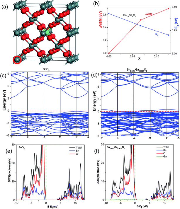
Additionally, because the absolute position of energy levels in a bulk calculation is ill-defined by DFT calculations, here we pick the deep core levels of a Ga atom (far from the doped Ga atom, see red cycled atom in Fig. 7(a)) to align the energy levels in different calculations.
Results and discussions
The XRD patterns of Ga-doped SnO2 calcined at 450 °C in air for 30 min are presented in Fig. 1(a). All of the undoped and the Ga-doped SnO2 have a tetragonal rutile crystal structure (PDF No. 77-0448) and no other crystalline forms are detected. As can be seen in the inset of Fig. 1(a), the diffraction peaks shift to higher theta values with increasing Ga3+ content to reveal a narrowing of the lattice constant in accordance with the Bragg equation: 2d![[thin space (1/6-em)]](https://www.rsc.org/images/entities/char_2009.gif) sin
sin![[thin space (1/6-em)]](https://www.rsc.org/images/entities/char_2009.gif) θ = λ, which can be attributed to the substitution of Sn4+ by Ga3+ because of the smaller effective radius of Ga3+(0.62 Å) compared to that of Sn4+(0.69 Å). In Fig. 1(b), the sizes of the SnO2 nanoparticles, as calculated by the Scherrer equation, decline from 15.85 nm to 13.79 nm as the amount of Ga3+ ions increases from 1 to 5 mol%. This is similar to the Al-doping cases, as the average diameter size of SnO2 decreases from ca. 16 nm to ca. 12 nm after the Al-doping.
θ = λ, which can be attributed to the substitution of Sn4+ by Ga3+ because of the smaller effective radius of Ga3+(0.62 Å) compared to that of Sn4+(0.69 Å). In Fig. 1(b), the sizes of the SnO2 nanoparticles, as calculated by the Scherrer equation, decline from 15.85 nm to 13.79 nm as the amount of Ga3+ ions increases from 1 to 5 mol%. This is similar to the Al-doping cases, as the average diameter size of SnO2 decreases from ca. 16 nm to ca. 12 nm after the Al-doping.
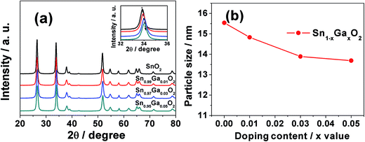 | ||
| Fig. 1 (a) XRD patterns of SnO2 and Ga-doped SnO2; (b) plots of doping content vs. particle size, derived using the Scherrer equation. | ||
The morphologies of the samples are studied by SEM as shown in Fig. 2(a) and (b). The as-synthesized SnO2 and Sn0.97Ga0.03O2 samples demonstrate the aggregated uniform hollow structure with a diameter of about 300 nm. These hollow nanospheres are assembled with SnO2 or Sn0.97Ga0.03O2 nanoparticles with shell thickness of about 80–100 nm confirmed by high-resolution TEM, as shown in Fig. 2(c) and (d). These morphologies are different from the hydrothermal synthesized Al-doped SnO2 nanoparticles, which show little aggregation. The HRTEM images show lattice fringes with regular spacings of 0.34 nm, which are associated with the (110) planes of SnO2 and Sn0.97Ga0.03O2. The well resolved fringes indicate that the SnO2 and Sn0.97Ga0.03O2 nanocrystals possess the high crystallinity.
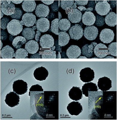 | ||
| Fig. 2 SEM images of (a) SnO2, and (b) Sn0.98Ga0.03O2. TEM, HR-TEM and FFT (inset) images of (c) SnO2, and (d) Sn0.97Ga0.03O2. | ||
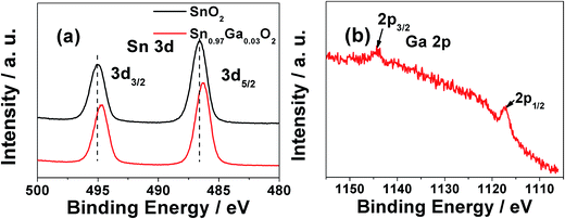
The binding energies of SnO2 and Sn0.97Ga0.03O2 samples were referenced to the C1s (284.8 eV) line measured by the XPS spectra (Fig. 3). The tin core levels Sn3d5/2 and Sn3d3/2 are observed at 486.05 and 494.50 eV, respectively, with a peak-to-peak separation of 8.45 eV. Compared with the pure SnO2 sample, a slight negative shift in binding energy was found from the Sn0.97Ga0.03O2 samples. The charge transfer occurring between two cationic species has been well studied with XPS for many mixed oxides, where the metallic ions are mixed at an atomic level, forming a heterogeneous linkage of M(A)–O–M(B) (where M(X) represents different metallic species). The electron cloud will be transferred from one type of cation to the other through their oxygen bridge in the linkage structure due to the different cation charge and electronegativity.43,44 In this case, the binding energy shift arises from electron transfer from Ga to Sn due to the differences of their electron negativity (electron negativity: Sn = 1.96, Ga = 1.81). The positions of Ga2p1/2 and Ga2p3/2 peaks are at 1118.1 and 1145.1 eV, respectively. These positions are in good agreement with the values previously reported by Schon, suggesting that Ga exists in the form of Ga3+.45
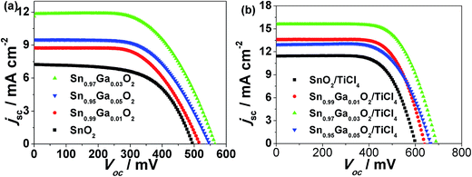
Fig. 4(a) shows the current density (J)–voltage (V) curves of DSSCs with the undoped SnO2 and Ga-doped SnO2 as the work electrode materials under simulated AM 1.5G illumination (100 mW cm−2). The photovoltaic performances, including the open circuit voltage (Voc), photocurrents (Jsc), fill factor (FF), and PCE, are summarized in Table 1. Although loading with less amount of dye, SnO2 nano hollow DSSC exhibits a higher efficiency than the DSSC based on SnO2 nanocrystal. The nano hollow SnO2 can enhance the light harvesting efficiency due to a higher light scattering ability than the SnO2 nanocrystal (Fig. S2†).46,47 Additionally, we can see that both Voc and Jsc are improved after Ga-doping, and the Ga-doped SnO2 electrodes showed a better performance than those of undoped SnO2 nano hollow spheres. The observed shifts of the flat band potential for the samples doped with 1 and 3 mol% of Ga are in agreement with the Voc variation. For the samples doped with 5 mol% of Ga, the decrease of the photovoltaic characteristics of the DSSCs is attributed to the decrease of the electrical conductance of the SnO2 films (Fig. S3†). And the overall performance of the films decrease due to the introduction of too many impurities. On the other hand, Jsc can be influenced by the light-harvesting efficiency, electrons injection rate, and charge recombination process. The light harvesting efficiency is a strong function of the dye loading. The Jsc factor for the given dye and cell design can be determined by:  . As shown in Table S2,† the dye loading amount increases with the increasing doping content (mainly due the increasing of specific surface area, Table 2), which partially contributed to the Jsc enhancement. According to the Katoh's report,48 the injection efficiency from excited N3 dyes to the conduction band of SnO2 are very high, suggesting that the injection process is not a limiting process for Jsc. Therefore, to improve the charge collection efficiency will be the additional approach to increasing Jsc (which will be discussed later). To further improve the performance of the DSSCs, we treated the electrode films with TiCl4. When TiCl4 modifies the photoanode films, the performance of DSSCs is optimized and the efficiency of the Sn0.97Ga0.03O2 photoanode reaches up to 7.11%, which is larger than that for our previous Al-doped SnO2 DSSCs (6.91%) and one of the highest so far to compare with the other reported high values for SnO2 based DSSCs (Table S1†). The photovoltaic parameters are indicated in Table S2† to compare with the DSSCs with and without TiCl4 treatment.
| Jsc (mA cm−2) | Voc (mV) | η (%) | FF | Dye loading (×10−7 mol cm−2) | |
|---|---|---|---|---|---|
| a Ref. 31. | |||||
| Nano-SnO2a | 7.92 | 467 | 2.03 | 0.55 | 0.77 |
| SnO2 | 7.23 | 496 | 2.13 | 0.60 | 0.62 |
| Sn0.99Ga0.01O2 | 8.73 | 517 | 2.68 | 0.60 | 0.70 |
| Sn0.97Ga0.03O2 | 11.62 | 565 | 3.84 | 0.59 | 0.74 |
| Sn0.95Ga0.05O2 | 9.50 | 547 | 2.96 | 0.57 | 0.76 |
| SnO2/TiCl4 | 11.42 | 601 | 4.67 | 0.68 | 0.93 |
| Sn0.99Ga0.01O2/TiCl4 | 13.59 | 640 | 5.91 | 0.68 | 1.06 |
| Sn0.97Ga0.03O2/TiCl4 | 15.61 | 691 | 7.11 | 0.66 | 1.11 |
| Sn0.95Ga0.05O2/TiCl4 | 12.90 | 665 | 5.49 | 0.64 | 1.13 |
| Sample | BET SSA (m2 g−1) |
|---|---|
| SnO2 | 21.48 |
| Sn0.99Ga0.01O2 | 25.15 |
| Sn0.97Ga0.03O2 | 28.55 |
| Sn0.95Ga0.05O2 | 30.14 |
The charge transfer and recombination behavior in the SnO2 and Ga-doped SnO2 films was studied by analyzing the EIS spectra at open circuit voltage and the Nyquist plots as shown in Fig. 5. The EIS spectra are characterized by the presence of two semicircles in a Nyquist plot. The high frequency semicircle is resulted from the charge transfer resistance (Rct) at the interfaces of the electrolyte/counter electrode, while the low frequency one is related to the chemical capacitance of SnO2 and the charge recombination resistance (Rrec) between SnO2 and the electrolyte. We found that the Rrec increased with the raising Ga-doping content in SnO2 films, which resulted in the highest Jsc and Voc achieved for the Ga-doped cells.
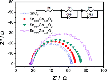 | ||
| Fig. 5 Nyquist plots of the cells with electrodes at open circuit. Inset shows the corresponding equivalent circuit. | ||
To further analyze the dynamics of electron transport and charge recombination of the DSSCs, intensity-modulated photocurrent spectroscopy (IMPS) and intensity-modulated photovoltage spectroscopy (IMVS) are performed as shown in Fig. 6. The IMVS shows that the lifetime or recombination time (τn) of the Ga-doped SnO2 is larger than that of the undoped SnO2, which is indicative of the higher photovoltage of the Ga-doped SnO2 than that of undoped SnO2, in agreement with the results of EIS measurement. This result is similar to the Al-doping cases, which also show an enlarged electron lifetime, but the degree is a little smaller for Ga-doping, indicating a more effective charge recombination suppression for Al-doping. However, the transport time (τd) of the Ga-doped SnO2 based cells increases with the increasing Ga-doping content, indicating a more slowly electron transport than that of the undoped SnO2 based cell. The increased τd after Ga-doping is similar to that for the Al-doping cases, but the increasing degree is slighter for Ga-doping. The τd increases from 17.9 ms to 40 ms when the Al content increases from 0 to 3 mol%, but the τd only increases from 15.2 ms to 21.1 ms when the Ga content increases from 0 to 5 mol%. The charge collection efficiency (ηcc) was introduced to quantitative analysis of the effect of transport time and electron lifetime. The ηcc of the DSSCs can be calculated according to the relation: ηcc = 1 − (τd/τn). The obtained ηcc value for SnO2, Sn0.99Ga0.01O2, Sn0.97Ga0.03O2, and Sn0.95Ga0.05O2 were 95.9%, 97.2%, 98.1%, and 97.8%, respectively. Thus, the higher ηcc value for Ga-doped SnO2 cells can result in a higher short circuit current (Jsc) density than that of the undoped SnO2 for DSSCs.
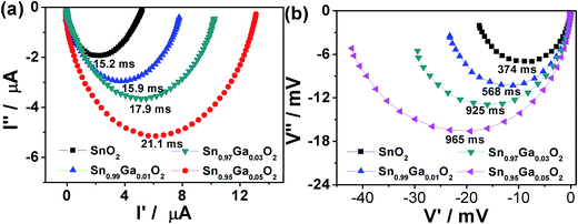 | ||
| Fig. 6 Complex plane plots and the corresponding time constant of the pure-SnO2 and Ga-doped SnO2 cells obtained from (a) IMPS and (b) IMVS. | ||
Density functional theory (DFT) calculations were performed for our materials to explore the effect of Sn atoms partially substituted by the Ga atoms. Fig. 7(a) shows the doping model. For each x value, we have considered at least four substitution structures and found out that the uniform doping is the most energy stable doping style. The calculated lattice parameters of bulk SnO2 are listed in Table S2.† The lattice parameters for the pure SnO2 agree well with experimental results, and they reduce a little after Ga doping due to the smaller ionic radius of Ga. Fig. 7(b)–(d) show the band structures and density of states (DOS) for pure SnO2 and Ga doped SnO2. The calculated band gap of SnO2 is 3.43 eV, close to the experimental value of 3.597 eV. From Fig. 7, our calculation clearly revealed a gradual upward (to high energies) shift for the valence and conduction band with Sn substituted by Ga. The Fermi level shifts positively (downward) to the valence band shows there is an p-type doping effect when Sn substituted by Ga for SnO2, which is attributed to that the heterovalent substitution of Sn atoms (4+) by Ga atoms (3+) introduces charge holes at the Ga sites. The band gap is also reduced a little when the Sn atoms are substituted by the Ga atoms (Fig. 7(b)). The upward shift for the conduction band minimum (CBM) is consistent with our experimental observation that the conduction band shifts negatively (upward) after Ga doping and increased Voc was obtained. At the same time, the p-type doping effect and the reduced band gap would increase the electrical conductance, which is consistent with the increased Jsc when the Ga doping content is increased from 0 to 3 mol%. According to the equation σ = neμ (n is the carrier concentration, μ is the carrier mobility), the electrical conductance of SnO2 would be increased after Ga doping under low content, due to the increased hole concentration. However, the increasing Ga contents could also introduce more impurity scattering centers to impede the electron transport (μ), and this effect would even dominate to reduce the whole electrical conductance when the Ga doping content exceeds some content. This is consistent with the increased electron transport time (τd) observed in the IMPS measurements and also accounts for the reduced Jsc when the Ga doping content is increased from 3 mol% to 5 mol%. It's hard to give a clear and direct relationship between the p-type doping effect and the suppressed charge recombination in Ga-doped SnO2 DSSCs experimentally and theoretically. The most probable reason accounting for this is that the heterovalent Ga doping introduces charge holes (p-type doping) in the bulk and surface of SnO2. These charge holes can attract electrons and act like charge trapping sites, to suppress the recombination between the electrons transferred from adsorbed dyes and the holes of the dyes and the redox mediator (I−/I3−) in the electrolyte. In our previous work, the Al doping shows a more effective charge recombination suppression.31 This is attributed to that a surface Al2O3 layer was formed on Al-doped SnO2, which acts as a thin coated insulating layer and increases the interface resistance greatly to further inhibit the electron–hole recombination.
Conclusions
In summary, by introducing the rough hollow microspheres structure and Ga-doping technique, the highest power conversion efficiency (η) up to 7.11% is obtained, which is larger than that for our previous Al-doped SnO2 DSSCs (6.91%) and one of the highest overall photoconversion efficiency for SnO2 based DSSCs. The Ga-doping results in a negative shift of the CB and the reduction of charge recombination so as to significantly enhance Jsc and Voc. The highest power conversion efficiency (η) under AM1.5 simulated solar illumination (100 mW cm−2) is obtained at the Ga doping amount of 3 mol%. These findings provide a new route to enhance the performance of DSSCs by improving the two key factors, such as to tune the energy levels of SnO2 and to retard charge recombination.Acknowledgements
This research was supported by Shenzhen Science and Technology Research Grant (No. ZDSY20130331145131323, JCYJ20120614150201123, SGLH20120928095706623 and JCYJ20120614150338154), National Natural Science Foundation of China (Grant No. 51303186), and National Research Fund for Fundamental Key Project (2012CB932903). Additionally, we acknowledge the support of ShenZhen National Super Computing Center.References
- J. Preat, D. Jacquemin and E. A. Perpete, Energy Environ. Sci., 2010, 3, 891–904 CAS.
- A. Hagfeldt, G. Boschloo, L. Sun, L. Kloo and H. Pettersson, Chem. Rev., 2010, 110, 6595–6663 CrossRef CAS.
- A. Yella, H. W. Lee, H. N. Tsao, C. Yi, A. K. Chandiran, M. K. Nazeeruddin, E. W. G. Diau, C. Y. Yeh, S. M. Zakeeruddin and M. Grätzel, Science, 2011, 334, 629–634 CrossRef CAS.
- W. Guo, Y. Shen, L. Wu, Y. Gao and T. Ma, J. Phys. Chem. C, 2011, 115, 21494–21499 CAS.
- K. Park, Q. Zhang, B. B. Garcia, X. Zhou, Y. H. Jeong and G. Cao, Adv. Mater., 2010, 22, 2329–2332 CrossRef CAS.
- J. Xiao, Q. Huang, J. Xu, C. Li, G. Chen, Y. Luo, D. Li and Q. Meng, J. Phys. Chem. C, 2014, 118, 4007–4015 CAS.
- J. Huo, Y. Hu, H. Jiang, W. Huang and C. Li, J. Mater. Chem. A, 2014, 2, 8266–8272 CAS.
- F. Lenzmann, J. Krueger, S. Burnside, K. Brooks, M. Gratzel, D. Gal, S. Ruhle and D. Cahen, J. Phys. Chem. B, 2001, 105, 6347–6352 CrossRef CAS.
- Z. D. Li, Y. Zhou, J. Y. Zhang, W. G. Tu, Q. Liu, T. Yu and Z. G. Zou, Cryst. Growth Des., 2012, 12, 1476–1481 CAS.
- Y. Furubayashi, T. Hitosugi and Y. Yamamoto, Appl. Phys. Lett., 2005, 86, 252101 CrossRef.
- J. F. Qian, P. Liu, Y. Xiao, Y. Jiang, Y. L. Cao, X. P. Ai and H. X. Yang, Adv. Mater., 2009, 21, 3663 CrossRef CAS.
- M. K. I. Senevirathna, P. Pitigala, E. V. A. Premalal, K. Tennakone, G. R. A. Kumara and A. Konno, Sol. Energy Mater. Sol. Cells, 2007, 91, 544–547 CrossRef CAS.
- H. C. Pang, H. B. Yang, C. X. Guo and C. M. Li, ACS Appl. Mater. Interfaces, 2012, 4, 6261–6265 CAS.
- M. H. Kim and Y. U. Kwon, J. Phys. Chem. C, 2011, 115, 23120–23125 CAS.
- E. Ramasamy and J. Lee, J. Phys. Chem. C, 2010, 114, 22032–22037 CAS.
- S. Gubbala, V. Chakrapani, V. Kumar and M. K. Sunkara, Adv. Funct. Mater., 2008, 18, 2411–2418 CrossRef CAS.
- X. C. Dou, D. Sabba, N. Mathews, L. H. Wong, Y. M. Lam and S. Mhaisalkar, Chem. Mater., 2011, 23, 3938–3945 CrossRef CAS.
- K. Perera, S. G. Anuradha, G. R. A. Kumara, M. L. Paranawitharana, R. M. G. Rajapakse and H. M. N. Bandara, Electrochim. Acta, 2011, 56, 4135–4138 CrossRef CAS.
- P. Docampo, P. Tiwana, N. Sakai, H. Miura, L. Herz, T. Murakami and H. J. Snaith, J. Phys. Chem. C, 2012, 116, 22840–22846 CAS.
- C. T. Gao, X. D. Li, B. G. Lu, L. L. Chen, Y. Q. Wang, F. Teng, J. T. Wang, Z. X. Zhang, X. J. Pan and E. Q. Xie, Nanoscale, 2012, 4, 3475–3481 RSC.
- H. Wang, B. Li, J. Gao, M. Tang, H. B. Feng, J. H. Li and L. Guo, Crystengcomm, 2012, 14, 5177–5181 RSC.
- Y. F. Wang, K. N. Li, C. L. Liang, Y. F. Hou, C. Y. Su and D. B. Kuang, J. Mater. Chem., 2012, 22, 21495–21501 RSC.
- P. N. Zhu, M. V. Reddy, Y. Z. Wu, S. J. Peng, S. Y. Yang, A. S. Nair, K. P. Loh, B. V. R. Chowdari and S. Ramakrishna, Chem. Commun., 2012, 48, 10865–10867 RSC.
- R. Kasaudhan, H. Elbohy, S. Sigdel, Q. Hui, W. Qufu and Q. Qiquan, IEEE Electron Device Lett., 2014, 35, 578–580 CrossRef CAS.
- X. Zou, X. Liu, C. Wang, Y. Jiang, Y. Wang, X. Xiao, J. C. Ho, J. Li, C. Jiang, Q. Xiong and L. Liao, ACS Nano, 2012, 7, 804–810 CrossRef.
- Q. Zhao, P. Wu, B. L. Li and E. Y. Jiang, Phys. Rev. B: Condens. Matter, 2012, 407, 171–174 CrossRef CAS.
- S. H. Park, J. B. Park and P. K. Song, Curr. Appl. Phys., 2010, 10, S488–S490 CrossRef.
- X. Lü, X. Mou, J. Wu, D. Zhang, L. Zhang, F. Huang, F. Xu and S. Huang, Adv. Funct. Mater., 2010, 20, 509–515 CrossRef.
- K. P. Wang and H. Teng, Phys. Chem. Chem. Phys., 2009, 11, 9489–9496 RSC.
- J. J. Teh, S. L. Ting, K. C. Leong, J. Li and P. Chen, ACS Appl. Mater. Interfaces, 2013, 5, 11377–11382 CAS.
- Y. Duan, J. Zheng, N. Fu, Y. Fang, T. Liu, Q. Zhang, X. Zhou, Y. Lin and F. Pan, J. Mater. Chem. A, 2015, 3, 3066–3073 CAS.
- P. Bonhôte, A. P. Dias, N. Papageorgiou, K. Kalyanasundaram and M. Grätzel, Inorg. Chem., 1996, 35, 1168–1178 CrossRef.
- P. E. Blochl, Phys. Rev. B: Condens. Matter Mater. Phys., 1994, 50, 17953–17979 CrossRef.
- G. Kresse and D. Joubert, Phys. Rev. B: Condens. Matter Mater. Phys., 1999, 59, 1758–1775 CrossRef CAS.
- J. Heyd, G. E. Scuseria and M. Ernzerhof, J. Chem. Phys., 2003, 118, 8207 CrossRef CAS.
- J. Heyd, G. E. Scuseria and M. Ernzerhof, J. Chem. Phys., 2006, 124, 219906 CrossRef.
- G. Kresse and J. Furthmuller, Phys. Rev. B: Condens. Matter Mater. Phys., 1996, 54, 11169–11186 CrossRef CAS.
- G. Kresse and J. Furthmuller, Comput. Mater. Sci., 1996, 6, 15–50 CrossRef CAS.
- J. Paier, M. Marsman, K. Hummer, G. Kresse, I. C. Gerber and J. G. Ángyán, J. Chem. Phys., 2006, 124, 154709 CrossRef CAS.
- J. P. Perdew, K. Burke and M. Ernzerhof, Phys. Rev. Lett., 1996, 77, 3865–3868 CrossRef CAS.
- J. B. Varley, A. Janotti and C. G. Van de Walle, Phys. Rev. B: Condens. Matter Mater. Phys., 2010, 81, 245216 CrossRef.
- D. O. Demchenko, B. Earles, H. Y. Liu, V. Avrutin, N. Izyumskaya, Ü. Özgür and H. Morkoç, Phys. Rev. B: Condens. Matter Mater. Phys., 2011, 84, 075201 CrossRef.
- T. L. Barr, M. A. Lishka, L. M. Chen and M. Mohsenian, J. Am. Chem. Soc., 1988, 110, 7962–7975 CrossRef CAS.
- J. Li and H. C. Zeng, J. Am. Chem. Soc., 2007, 129, 15839–15847 CrossRef CAS.
- G. Schon, J. Electron. Spectrosc. Relat. Phenom., 1973, 2, 75–86 CrossRef CAS.
- J. Xing, W. Q. Fang, Z. Li and H. G. Yang, Ind. Eng. Chem. Res., 2012, 51, 4247–4253 CrossRef CAS.
- S. Yang, Y. Hou, J. Xing, B. Zhang, F. Tian, X. H. Yang and H. G. Yang, Chem.–Eur. J., 2013, 19, 9366–9370 CrossRef CAS.
- R. Katoh and A. Furube, J. Photochem. Photobiol., C, 2014, 20, 1–16 CrossRef CAS.
Footnotes |
| † Electronic supplementary information (ESI) available: Mott–Schottky plots of the SnO2 and the Ga-doped SnO2 films. Diffuse reflectance spectra of the photoelectrodes with nano SnO2, nano hollow SnO2 and nano hollow Sn0.97Ga0.03O2. Specific resistivity as a function of doping level for Sn1−xGaxO2 films. Normalized device performance under constant illumination for 100 h measured in air. Elemental mapping of the Sn0.97Ga0.03O2. Calculated total and orbital resolved densities of states for the pure SnO2 and 6.25% Ga doped SnO2. The reported high values of η obtained in the DSSCs based on different SnO2 photoanode structures. Calculated structural parameters a and c for pure SnO2 and 6.25% Ga doped SnO2. See DOI: 10.1039/c5ra19491a |
| ‡ These authors contributed equally to this work. |
| This journal is © The Royal Society of Chemistry 2015 |

