
 Open Access Article
 This Open Access Article is licensed under a Creative Commons Attribution-Non Commercial 3.0 Unported Licence
Psychological tactile sensor structure based on piezoelectric nanowire cell arrays
Yeri
Jeong
ac,
Minkyung
Sim
a,
Jeong Hee
Shin
a,
Ji-Woong
Choi
a,
Jung Inn
Sohn
b,
Seung Nam
Cha
b,
Hongsoo
Choi
d,
Cheil
Moon
e and
Jae Eun
Jang
*ad
aDepartment of Information & Communication Engineering, Daegu Gyeongbuk Institute of Science & Technology (DGIST), Daegu 711-873, Korea. E-mail: jang1@dgist.ac.kr
bDepartment of Electrical Engineering Science, University of Oxford, Park Road, Oxford, OX1 3PJ, UK
cSamsung Display, Yongin 449-712, Korea
dDepartment of Robotics Engineering, DGIST-ETH Microrobot Research Center, Daegu Gyeongbuk Institute of Science & Technology (DGIST), Daegu 711-873, Korea
eDepartment of Brain & Cognitive Sciences, Daegu Gyeongbuk Institute of Science & Technology (DGIST), Daegu 711-873, Korea
First published on 17th April 2015
Abstract
To produce artificial psychological feeling, especially ‘pain’, an electrical structure that mimics human skin has been studied. Touch by a sharp and a blunt object induces different deformations of the skin of human fingers. In order to imitate this phenomenon, a skin-mimicking device employing piezoelectric nanowire sensor arrays is used to generate an electrical ‘pain’ signal with signal processing when a pen cap presses the device. The electrical ‘pain’ signal is expected to enhance the protection mechanism of an android robot or mobile phone against harsh environments.
Recently, artificial tactile sensors have been studied in attempts to mimic the human sense of touch for various applications, from the simple input function of mobile devices to the complicated finger systems of android robots.1–8 Unfortunately, most touch sensors that have been developed so far simply detect pressure without the generation of psychological feelings or focus on achieving grip control, to hold an egg or some other fragile object. For human beings, feelings such as softness, roughness or pain are important for interactions with other humans and objects. Furthermore, pain is an essential feeling that protects the human body from sharp objects such as a knife, a needle, or a nail. Therefore, if we can develop an artificial tactile sensor, which can generate an electrical pain signal, an android robot hand or a mobile phone touch display can be better protected from contact with sharp objects or from harsh environments.
Herein, we report tactile sensor arrays and signal processing based on ZnO piezoelectric nanowires, which produce feelings of artificial psychological pain. Tactile sensors based on ZnO piezoelectric materials have several advantages, such as being self-powered, highly sensitive, high resolution, multi-touch availability, and simple design. To get a high sensitivity of touch, the piezoelectric characteristics of ZnO nanowires, including the effects of nanowire structural factors, have been studied using various metal electrodes. By signal processing of the detected signals based on a pattern analysis and its pressure level, the proposed artificial tactile sensor structure was able to successfully produce an electrical pain signal from the touch of a sharp object.
Fig. 1 shows a schematic of how to produce an electrical pain signal using our suggested device structure. As shown in the figure, the skin of a human finger deforms differently according to the shape of the object touching it: a pencil lead produces a high pressure on a very small area of skin, whereas a pencil eraser deforms a larger skin area. Because humans have several types of touch receptors in the skin, and the signals from these receptors can arouse a ‘pain’ signal as well as a ‘soft’ and a ‘rough’ feeling in the nervous system,9,10 it is not easy to mimic a human system perfectly using a simple artificial device design. However, if a proper electro-mechanical structure design can mimic the different deformations, it can produce a simple pain signal. Although it is just a simple pain signal, it can be useful in protecting the device from harsh objects. To achieve this goal, electromechanical pressure sensor array structures and signal processing approaches are suggested. By distributing a number of active sensors, a sensor array device can detect different pressure levels, such as the prick of a pencil lead or the press of a pencil eraser in a manner similar to the deformation of human skin. When the system is pricked with the pencil lead, a single cell or a few cells will be activated with a high pressure signal but in the case of the pencil eraser, multiple touch pressure signals will be produced by the centre and the neighbouring cells (Fig. 1 right side illustration). By signal processing of the detected signals based on a pattern analysis and a threshold pressure limit, an artificial pain signal can be generated in the case of a pencil lead.
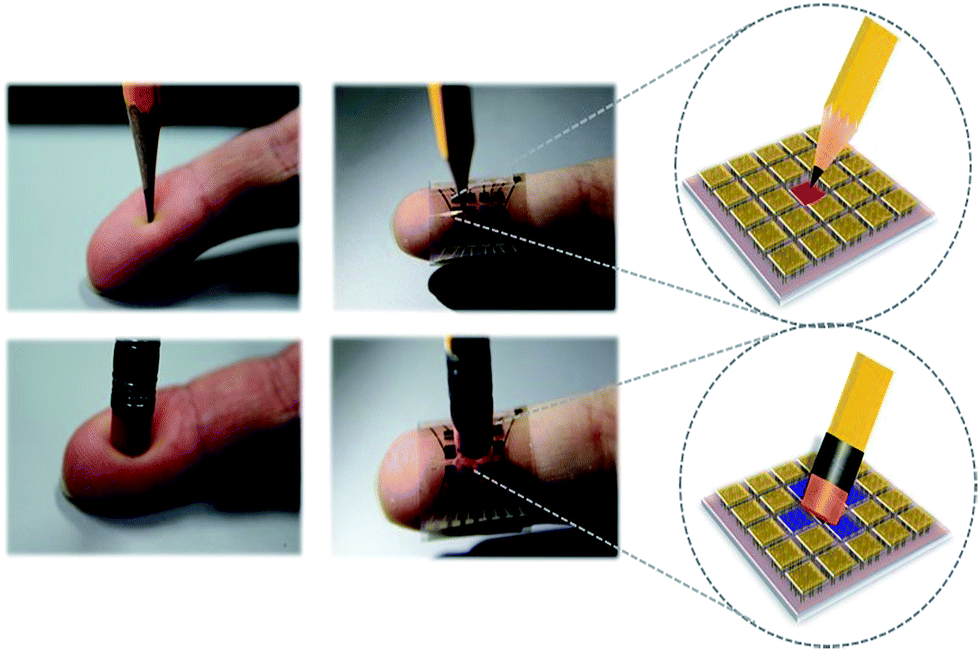 | ||
| Fig. 1 Schematic of how to produce an electrical ‘pain’ signal by touch sensor arrays. The pressure levels and the distribution shape of activated cells induce ‘pain’ or ‘smooth’ feeling signals. | ||
For pressure sensor arrays, various principles can be applied to detect pressure levels. Resistive and capacitive type touch sensors have been recently developed and widely adopted in smart phones and tablet PCs.11,12 Although these approaches have various merits, the simple matrix resistive type is limited for multi-touch applications due to cross-talk issues, and the capacitive type has a low pressure sensitivity, which can be barriers to our suggested working principle. Among other mechanisms, a piezoelectric sensor structure is a good candidate for our proposed system because it has good spatial resolution, multi-touch ability, and excellent pressure sensitivity. Moreover, since it can produce electrical power or a signal by itself due to the piezoelectric effect, which consumes no power, the mechanism is ideal for an android robot or smart phone, which needs a battery to work independently. Pb[Zr,Ti]O3 (PZT) has been well known as a high piezoelectric coefficient material and has been studied widely. However, the high processing temperature of PZT (∼600 °C) limits its use with flexible substrates because most flexible substrates are vulnerable to a high heat environment.13 To apply the sensor array concept to the finger of an android robot or wearable device, the device substrate should also be flexible. Considering various aspects of device structure and characteristics, ZnO nanowire was selected for our device structure. ZnO nanowires are easily grown by a hydro-thermal process below 90 °C; hence, the process can be applied to most flexible substrates and the cost of the fabrication process is lower than that of vacuum deposition processes. Moreover, unlike the low piezoelectric coefficient of ZnO bulk film, the ZnO nanowire structure has a relatively high piezoelectric coefficient due to the structural confinement of the nanowires in the radial direction. Therefore, ZnO nanowire was deliberately selected for use in the proposed high sensitivity pressure detector system.14–16
To enhance the signal to noise ratio of the ZnO nanowire pressure sensor structure, the characteristics of the piezoelectric effect were studied using various metal electrodes. Under an applied force, a net dipole moment is induced in a ZnO nanowire. Due to the net dipole moment, electrical charges accumulate on the top and the bottom electrodes of the sensor structure, which results in the flow of piezoelectric current. Since ZnO is a wide band gap semiconductor,17,18 an electrical barrier structure between the ZnO nanowire and the metal electrode can improve the current level by preventing hole–electron recombination at the boundary of the electrodes. A Schottky barrier provides the appropriate solution due to its simple fabrication process. For comparison, three types of electrode, Au, Nb, and Ni, were used as the bottom electrodes of a device structure. A hydrothermal method was employed to grow ZnO nanowires on these metal layers. The nutrient solution was composed of a 1![[thin space (1/6-em)]](https://www.rsc.org/images/entities/char_2009.gif) :1 ratio of zinc nitrate and hexamethylene tetramine (HMTA). The process temperature was set at 90 °C. As shown in Fig. 2a, ZnO nanowires grew well on the metal electrodes with slightly different forms of growth. All the ZnO nanowires are similar in length and diameter. However, the vertical alignment of the nanowires is a little different. The ZnO nanowires on the Au layer are aligned vertically, whereas some nanowires on the Nb and Ni layers are tilted slightly. Considering the vector field of the electrical dipole moment induced by the piezoelectric effect, good vertical alignment can generate a higher electrical signal. Thin ZnO film (50 nm) formed by a RF magnetron sputtering system at room temperature was used as a seed layer for the growth of the ZnO nanowires. The working pressure and the power of sputtering are 1 × 10⁻² Torr and 200 W, respectively. As shown in the XRD analyses of the seed layers on various metal layers, the seed crystals in ZnO film on a Au layer have a higher level of preferred orientation to the (002) direction (Fig. 2b), which results in the nanowires on the Au layer having a higher probability of growing vertically. The calculated Schottky barrier heights of Au, Nb, and Ni are 0.9 eV, 0.1 eV, and 0.81 eV, respectively. The current–voltage (I–V) curves of the three metals employed as bottom electrodes correspond well to the barrier heights (Fig. 2c). Au and Ni cases show an asymmetric I–V characteristic due to Schottky barrier formation, whereas the Nb layer forms an ohmic-like contact.
:1 ratio of zinc nitrate and hexamethylene tetramine (HMTA). The process temperature was set at 90 °C. As shown in Fig. 2a, ZnO nanowires grew well on the metal electrodes with slightly different forms of growth. All the ZnO nanowires are similar in length and diameter. However, the vertical alignment of the nanowires is a little different. The ZnO nanowires on the Au layer are aligned vertically, whereas some nanowires on the Nb and Ni layers are tilted slightly. Considering the vector field of the electrical dipole moment induced by the piezoelectric effect, good vertical alignment can generate a higher electrical signal. Thin ZnO film (50 nm) formed by a RF magnetron sputtering system at room temperature was used as a seed layer for the growth of the ZnO nanowires. The working pressure and the power of sputtering are 1 × 10⁻² Torr and 200 W, respectively. As shown in the XRD analyses of the seed layers on various metal layers, the seed crystals in ZnO film on a Au layer have a higher level of preferred orientation to the (002) direction (Fig. 2b), which results in the nanowires on the Au layer having a higher probability of growing vertically. The calculated Schottky barrier heights of Au, Nb, and Ni are 0.9 eV, 0.1 eV, and 0.81 eV, respectively. The current–voltage (I–V) curves of the three metals employed as bottom electrodes correspond well to the barrier heights (Fig. 2c). Au and Ni cases show an asymmetric I–V characteristic due to Schottky barrier formation, whereas the Nb layer forms an ohmic-like contact.
 | ||
| Fig. 2 ZnO nanowires grown on various metal layers. (a) SEM images of ZnO nanowires on Au, Nb, and Ni. The scale bar corresponds to 1 μm. (b) XRD analysis results of ZnO seed layers on various metals. (c) I–V characteristics with different metal layers. (d) The piezoelectric voltage of an ZnO sensor array using different metal bottom electrodes. Applied pressure level is 25 kPa. | ||
To measure the piezoelectric characteristics of ZnO nanowire on various metal layers, an ITO coated PEN film was placed on the ZnO nanowires as an upper electrode. The sensor structure employing Au shows the highest signal to noise ratio (Fig. 2c). This is reasonable taking into account the Schottky barrier height and the vertical alignment of nanowires. For a bulk cylindrical piezoelectric generator, induced voltage is simply expressed in terms of applied force. If the applied stress is T, then the induced polarization P is
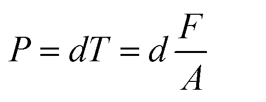 | (1) |
Induced polarization, P, leads to induced surface polarization charges given by Q = AP. If C is capacitance, then the induced voltage is
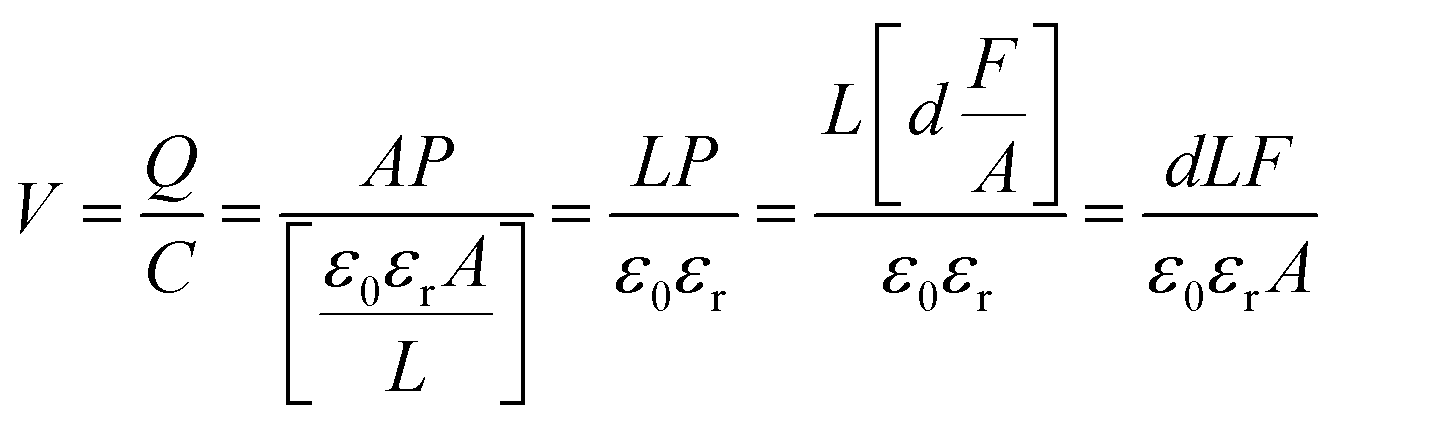 | (2) |
Fig. 3 shows the pressure sensitivities associated with various ZnO nanowire structural dimensions. Because the growth rate of the nanowires in the radial direction is slower than that in the longitudinal direction, a long growth time, which results in a longer ZnO nanowire, does not guarantee higher sensitivity due to an increase in diameter. To find the optimal ZnO structural dimensions, pressure sensitivity was measured for three different ZnO nanowire growth times. With increasing growth times up to 72 h, the length of the nanowires increased; however, the growth rate decreased slightly. Due to an increase in radial direction growth, the 48 h growth time gives the highest aspect ratio of length to diameter (Fig. 3a and b). From these structural differences, signal levels, represented by piezoelectric voltages, are changed. As expected, the ZnO nanowires grown for 48 h with the highest structural aspect ratio lead to better pressure sensitivity over the entire pressure range.
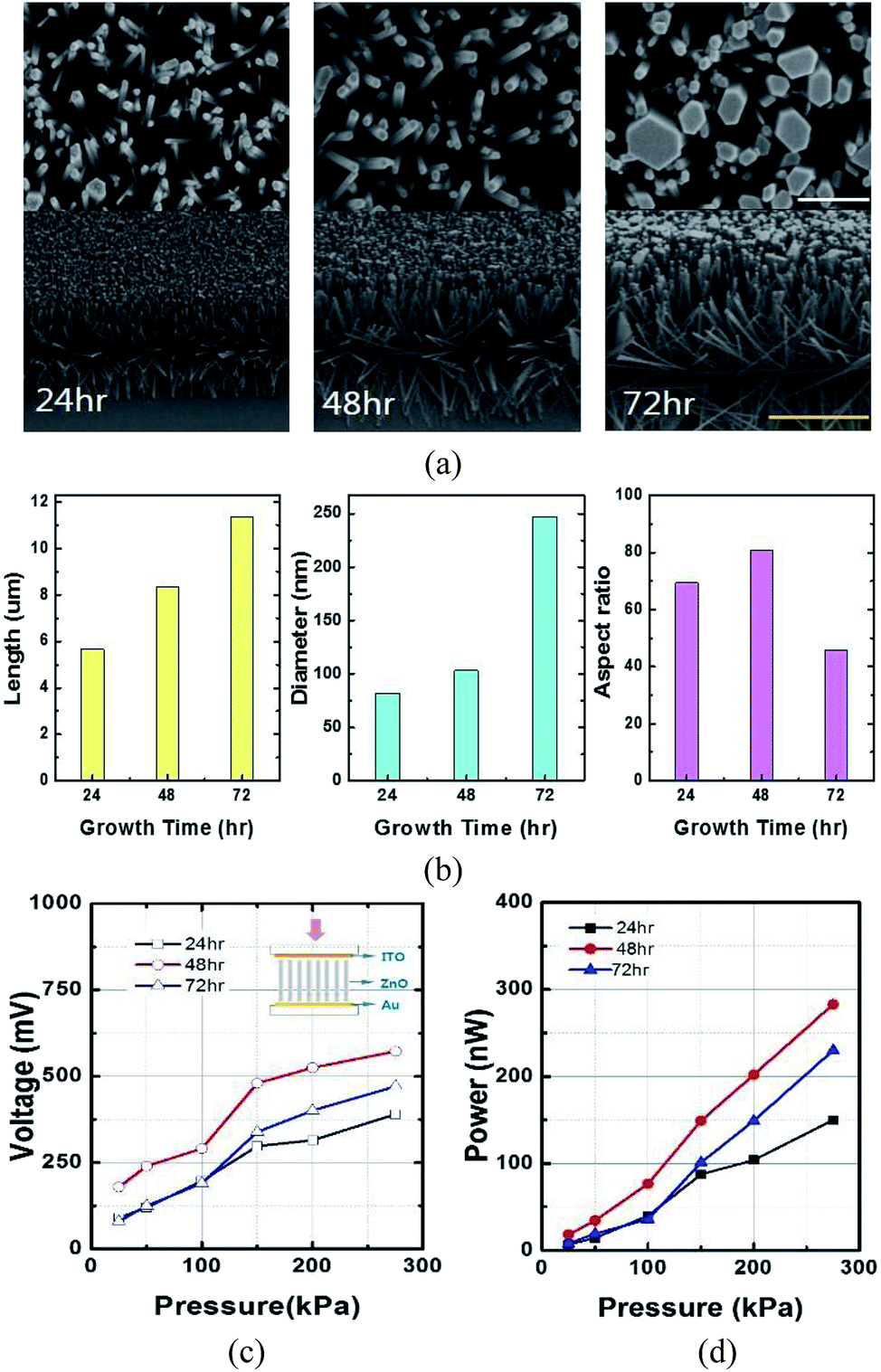 | ||
| Fig. 3 Pressure sensitivities associated with various structural dimensions of ZnO nanowire (a) SEM images of ZnO nanowires grown for 24 h, 48 h, and 72 h; the white and the yellow scale bars correspond to 1 μm and 10 μm, respectively. (b) Dimensional values of ZnO nanowires for different growth times, average length, average diameter, and aspect ratio of length to diameter. (c) Peak voltages generated by various pressures. (d) Electrical power produced by pressure. | ||
Although the electrical voltage level produced by all the ZnO nanowire cells is enough to be detected by a general electrical sensing circuit in the low pressure range, considering power consumption, reliability, and durability, a growth time of 48 h was determined to be an optimal condition for the psychological tactile sensor structure. Since the generated voltage levels are changed within test pressure levels without a saturation, the ZnO nanowire sensor structure is appropriate for the pressure sensor application. For a growth time of 72 h, the SEM image shows a large deviation of the nanowire diameters. A few nanowires have abnormal diameters, whereas most of the nanowires show a similar diameter or are slightly thicker than those grown for 48 h. For that reason, even though the average aspect ratio is lower than that for a growth time of 24 h, the ZnO nanowire structure grown for 72 h shows a better voltage level than that grown for 24 h. The power level produced is as high as 10 nW; hence, it is possible to detect the signal level without any other power consumption. This can be an important advantage for applications, such as an android robot and a smart phone, which need to work independently without being connected to a mains power supply.
To prove the concept of a psychological tactile sensor, 3 × 3 cell arrays employing ZnO nanowires were fabricated. As the top electrode of the sensor structure, Au thin film electrodes were formed on a PEN substrate, which resulted in aligned ZnO nanowires. Blunt objects, such as a pencil eraser and an earplug, were used to touch the centre of the cell arrays with different pressures, as shown in Fig. 4a. Within different pressure states, the electrical signals produced by the deformation of the ZnO nanowires in all cells were detected by the sensing system (Fig. 4b) and the levels changed the different colours on the visual image by simple image processing (Fig. 4c). The touch of the pencil eraser with a low pressure creates contact points on the centre area so that the centre cell (∼100 mV) and other neighbouring cells (∼50 mV) produce piezoelectric signals, whereas there are no signals detected for the other 4 corner cells since they are not in contact. The time between the red lines on the enlarged piezoelectric voltage graph of cell 5 indicates the length of time the pressure of the pencil eraser was maintained (Fig. 4b). With a piezoelectric material, no signal is generated when pressure is maintained over time at the same level. However, since the initial and the final touches induce current flows in the circuit system, we can deduce whether an object is still pressed onto the system or has detached from the device. When the pressure level is increased, the piezoelectric signals are also increased and the centre cell colours are changed to yellowish green and orange on the detection image. However, the other 4 corner cells that are not contacted do not generate any electrical power and keep their blue colour. For the centre cell, at the high pressure level, the piezoelectric voltage is about 250 mV. It can be noted that if only voltage was selected as the threshold evaluation factor to indicate a ‘pain’ signal from the device and its level was above 200 mV, the sensing device would produce a ‘pain’ signal even with the high pressure of an eraser, even though people do not normally feel pain for the same situation.
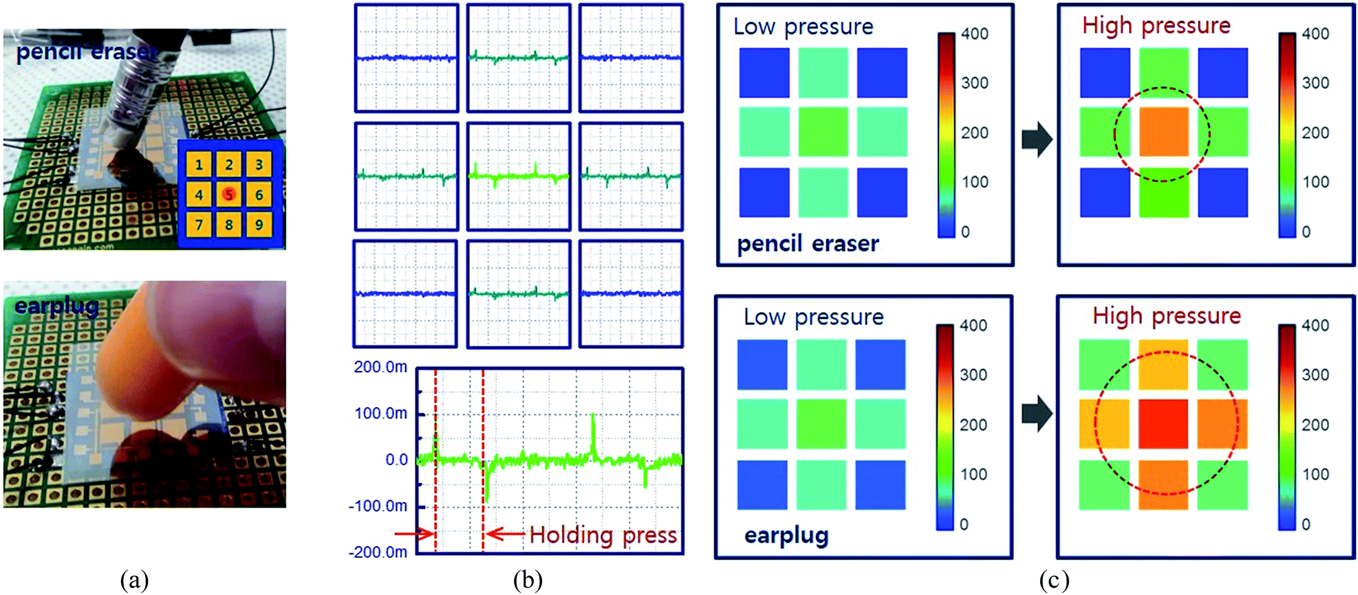 | ||
| Fig. 4 Pressure level images of the touch of a pencil eraser and an earplug for different pressure levels (a) photo images of touch by a pencil eraser and an earplug (b) piezoelectric voltages of 9 cells as a result of the touch of a pencil eraser (top) and the enlarged graph of the centre cell (bottom) for a low pressure touch (c) visual images of piezoelectric voltages depending on the touch object and the pressure level. The yellowish green colour matches approximately 100 mV. | ||
This is not the case with our system, because the device does not generate a ‘pain’ warning simply based on an electrical signal exceeding the threshold limit; moreover, signals from the other sensors in the array and their number and distribution are also part of the evaluation factor of the ‘pain’ feeling. Based on the sensing cell distribution and the signal levels, the system roughly recognizes the shape of an object, which is touching it, and the pressure level precisely. The signals from the other 4 edge cells provide the device with the information that the object touching it is not sharp like a needle. The earplug is bigger and much softer than the eraser, and so it contacts a larger area with the same pressure level. The different characteristics of the object can be easily detected by the visual image processing result. All 9 cells have their own signals due to the touch of earplug. A higher contact pressure generates higher electrical signals from the 5 centre region cells than the threshold limit voltage. However, due to the cell distribution, there is no ‘pain’ signal either. The red colour rings on the visual images mean that the potential inside the ring is higher than 100 mV. The ring area is well matched with the area contacted by the pencil eraser and the earplug. Therefore, we can estimate the shape of an object by the artificial tactile sensor structure as well.
Fig. 5 shows how to produce the ‘pain’ feeling with the touch of a pen cap. When the pen cap, which has a sharp shape, pressed the device with a low pressure, specifically at cell position 4, only that cell generated a piezoelectric signal. The detection level is similar to the level when the pencil eraser presses the device with a low pressure. Since the pen cap only touches cell 4, due to its sharp shape, the other cells do not generate any electrical signals. However, the signal level is lower than the set threshold voltage (>200 mV); hence, the ‘pain’ signal is not produced. As the pressure exerted by the pen cap increases, the piezoelectric voltage of cell 4 is increased to about 300 mV, whereas the other cells continue to generate no signal, unlike when the device is touched by a pencil eraser or an earplug. The visual images clearly show the touch situation, which differs from the touch of a pencil eraser or an earplug. Only cell 4 show a change of colour, from bluish-green to orange. With respect to the two evaluation factors, such as signal level and sensing cell distribution, the system recognizes that a sharp object is stabbing the device with a high force. Consequently, the device produces an electrical ‘pain’ warning signal. If the artificial tactile sensor system is applied to an android robot or a mobile phone, that electrical ‘pain’ signal could drive a protective mechanism in response to the touch of sharp objects. When humans touch their finger lightly with a needle, they do not have a ‘pain’ feeling, however, with a greater force, they feel ‘pain’ immediately. Therefore the phenomenon that induces the ‘pain’ feeling in the artificial device is similar to the mechanism by which humans feel pain. Because the response time of the ZnO nanowire sensor arrays is quite fast, the device structure is appropriate for use in the psychological tactile sensor and its various applications.
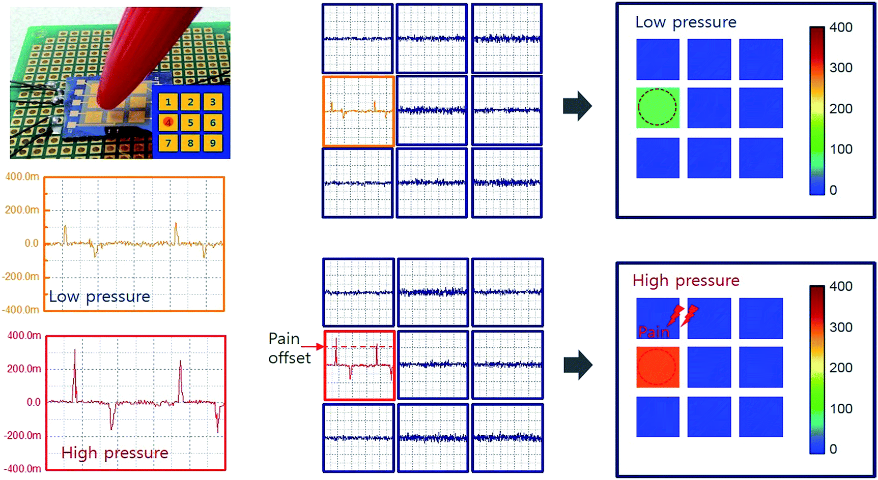 | ||
| Fig. 5 Pressure level visual images resulting from the touch of a pen cap with different pressure levels. The cap presses the cell 4 position (photo image). Among 9 cells, only cell 4 generates a piezoelectric signal (middle graph). The enlarged graph for cell 4 shows that the piezoelectric voltage changes with the pressure level (left graph). The visual image formed by the signal process clearly shows the active cell position with the signal level. | ||
Conclusions
To produce artificial psychological feelings, we tried to develop tactile sensor arrays and a signal processing mechanism based on ZnO piezoelectric nanowires. The sensors based on piezoelectric materials have several advantages such as self-powered, high resolution, multi touch, and simple design. The pressure value was evaluated easily from the electrical power produced by the ZnO nanowire structure. The array design of the self-powered tactile sensor allowed the pressure level and the figuration of the object touching the sensor to be perceived. With respect to two evaluation factors, the signal level and the sensing cell distribution, the system recognized that a sharp object stabbed the device with a high force, and then the device produced an electrical ‘pain’ warning signal. This suggested design and concept can be used in various new applications for electrical devices and the robot industry.Acknowledgements
This research was supported by Basic Science Research Program through the National Research Foundation of Korea (NRF) funded by the MEST (2014M3A9D7070668), MEST & DGIST (15-BD-0404) and the Korea Institute of Energy Technology Evaluation and Planning (KETEP) (20128510010080).Notes and references
- R. S. Dahiya, G. Metta, M. Valle and G. Sandini, IEEE Trans. Robot., 2010, 6, 1 CrossRef.
- H. Zhang and E. So, IEEE Trans. Syst. Man Cybern. B Cybern., 2002, 32, 57 CrossRef PubMed.
- K. Weiss and H. Worn, in Proc. IEEE Int. Conf. Manipulation Grasping, Genoa, Italy, vol. 1, 2004 Search PubMed.
- D. J. Beebe, A. S. Hsieh, D. D. Denton and R. G. Radwin, Sens. Actuators, A, 1995, 50, 55 CrossRef CAS.
- Z. Chu, P. M. Sarro and S. Middelhoek, Sens. Actuators, A, 1996, 54, 505 CrossRef.
- P. A. Schmidt, E. Mael and R. P. Wurtz, Robot. Autonom. Syst., 2006, 54, 1005 CrossRef.
- B. Zhu, Z. Niu, H. Wang, W. R. Leow, H. Wang, Y. Li, L. Zheng, J. Wei, F. Huo and X. Chen, Small, 2014, 10, 3625–3631 CrossRef CAS PubMed.
- Q. Shao, Z. Niu, M. Hirtz, L. Jiang, Y. Liu, Z. Wang and X. Chen, Small, 2014, 10, 1466–1472 CrossRef CAS PubMed.
- J. M. Wolfe, K. R. Kluender, D. M. Levi, L. M. Bartoshuk, R. S. Herz, R. L. Klatzky and S. J. Lederman, Sensation and Perception, Sinauer, Sunderland, MA, 2006 Search PubMed.
- D. S. Hecht, D. Thomas, L. Hu, C. Ladous, T. Lam, Y. Park, G. Irvin and P. Drzaic, J. Soc. Inf. Disp., 2012, 17, 941 CrossRef.
- T. Hwang, W. Cui, I. Yang and O. Kwon, IEEE Trans. Consum. Electron., 2010, 56, 1115 CrossRef.
- H. Yoshikawa and S. Adachi, Jpn. J. Appl. Phys., 1997, 36, 6237 CrossRef CAS.
- A. Gruverman, O. Auciello and H. Tokumoto, Appl. Phys. Lett., 1996, 69, 3191 CrossRef CAS.
- J. I. Sohn, Y. Jung, S. Baek, S. N. Cha, J. E. Jang, C. Cho, J. H. Kim, J. M. Kim and I. Park, Nanoscale, 2014, 6, 2046 RSC.
- S. Cha, S. M. Kim, H. Kim, J. Ku, J. I. Sohn, Y. J. Park, B. G. Song, M. H. Jung, E. K. Lee, B. L. Choi, J. J. Park, Z. L. Wang, J. M. Kim and K. Kim, Nano Lett., 2011, 11, 5142 CrossRef CAS PubMed.
- Y. Zhu, Y. Zhou, M. I. B. Utama, M. Mata, Y. Zhao, Q. Zhang, B. Peng, C. Magen, J. Arbiol and Q. Xiong, Nanoscale, 2013, 5, 7242 RSC.
- Z. L. Wang and J. H. Song, Science, 2006, 312, 242 CrossRef CAS PubMed.
- J. E. Jang, S. N. Cha, T. P. Butler, J. I. Son, J. W. Kim, Y. W. Jin, G. A. J. Amaratunga, J. M. Kim and J. E. Jung, Adv. Mater., 2009, 21, 4139 CrossRef CAS.
| This journal is © The Royal Society of Chemistry 2015 |