
Plasmon-enhanced light harvesting: applications in enhanced photocatalysis, photodynamic therapy and photovoltaics
Na Zhou
ab,
Vanesa López-Puente
c,
Qing Wang
d,
Lakshminarayana Polavarapu
*c,
Isabel Pastoriza-Santos
*c and
Qing-Hua Xu
*ab
aDepartment of Chemistry, National University of Singapore, Singapore 117543, Singapore. E-mail: chmxqh@nus.edu.sg
bNational University of Singapore (Suzhou) Research Institute (NUSRI), Suzhou, Jiangsu 215123, China
cDepartamento de Química Física, Facultade de Química, CINBIO, Universidad de Vigo, 36310 Vigo, Spain. E-mail: lakshmi@uvigo.es; pastoriza@uvigo.es
dDepartment of Materials Science and Engineering, National University of Singapore, Singapore 117576, Singapore
First published on 17th March 2015
Abstract
Plasmonic nanostructures have played a significant role in the development of modern materials science and technology. Plasmon-enhanced solar light harvesting to enhance the efficiency of solar to fuel energy conversion has been one of the most important research areas of the last decade to help meet the worlds growing energy demand. Over the years, both organic and inorganic semiconductor materials, with high stability, environmental compatibility and photocatalytic activity, have been widely used as photocatalysts for direct conversion of solar energy into fuels. However, the efficiency of semiconductors is limited by their inability to absorb visible light due to high band gap. During last few years, great amount of research has been carried out to improve the efficiency of photocatalysts and photovoltaic devices by integration of plasmonic nanoparticles (NPs) with semiconductor materials. The presence of plasmonic NPs leads to increase in the absorption cross-section of semiconductors via strong field enhancement, extension of light absorption to longer wavelengths and enhances electron–hole charge separation in semiconductor medium, thus maximize the efficiency of photocatalytic and photovoltaic devices. In this review, we summarize recent advances made toward the integration of plasmonic nanostructures with semiconductor photocatalytic systems for enhanced light harvesting applications, including dye degradation, water splitting for H2 generation, photodynamic therapy, chemical transformation and photovoltaics.
 Na Zhou | Na Zhou obtained her master degree from Nankai University (China) in 2010 and Ph.D. degree from the National University of Singapore (Singapore) in 2014 under the supervision of Prof. Qing-Hua Xu. Now she is currently a research associate in Department of Chemistry, National University of Singapore. Her main research interests include fabrication of plasmonic metal–semiconductor nanocomposites systems for photocatalytic and photovoltaic applications. |
 Vanesa López-Puente | Vanesa López-Puente obtained her chemistry degree from the Universidade da Coruña (Spain) in 2008. She is currently working on her Ph.D. degree under the supervision of Prof. Luis M. Liz Marzán at the University of Vigo (Spain). Her research is focused on synthesis and characterization of hybrid materials based on metal nanoparticles and mesoporous thin films for SERS detection. |
 Qing Wang | Qing Wang is an Associate professor at the Department of Materials Science and Engineering, National University of Singapore (NUS). He obtained his Ph.D. in condensed matter physics at Institute of Physics, Chinese Academy of Sciences in 2002. Before joined NUS, he has been working with Prof. Michael Grätzel at École Polytechnique Fédérale de Lausanne and Dr Arthur J. Frank at National Renewable Energy Laboratory in the field of mesoscopic photoelectrochemical cells. Currently he is leading a group to conduct fundamental and applied studies on charge transport in mesoscopic energy conversion and storage systems, including redox flow lithium-ion batteries. |
 Lakshminarayana Polavarapu | Lakshminarayana obtained his master degree from the University of Hyderabad (India) in 2005 and his Ph.D. degree from the National University of Singapore in 2011. He worked as a postdoctoral fellow at CIC biomaGUNE in San Sebastián (2012–2013), and he is currently a postdoctoral fellow at the University of Vigo (Spain). He is a co-author of over 40 publications and his current research interests include shape controlled synthesis of metal nanocrystals for applications such as plasmonic sensors, plasmonic solar cells and water splitting. |
 Isabel Pastoriza-Santos | Isabel Pastoriza-Santos obtained her Ph.D. degree from the Universidade de Vigo in 2001. She worked as a postdoctoral fellow at the University of Melbourne (Australia) in 2002 and 2003. Since 2009, she has been an Associate Professor at the University of Vigo. She has co-authored over 100 articles and holds 2 patents. Her current interests include the synthesis of plasmonic nanoparticles with size and shape control, as well as their assembly. |
 Qing-Hua Xu | Qing-Hua Xu obtained his B.S. degree from Zhejiang University (1993), M.S. degrees from Peking University (1996) and University of Chicago (1997), and Ph.D. degree from UC Berkeley (2001). He conducted his postdoctoral research at Stanford University (2001–2002) and UC Santa Barbara (2002–2005). He joined Department of Chemistry, National University of Singapore as an Assistant Professor in 2005 and has been an Associate Professor of the same university since 2011. He is a co-author of over 120 peer-reviewed publications. His current research interests include linear and nonlinear optical properties of nanocomposite materials and their applications in imaging, sensing, biomedicine and energy areas. |
1. Introduction
Solar light harvesting in an efficient manner is one of the most challenging problems, which is currently under intensive investigation by various researchers around the world to meet the world's future energy needs.1 Sunlight, being an abundant and easily available energy natural resource, possesses great potential in driving environmentally friendly photochemical transformations.2,3 Direct conversion of light energy into chemical energy or electricity using photocatalysts or photoactive materials have received great interest in recent years.1,3–10 Although a significant progress have been achieved in the development of efficient materials for enhanced photocatalysis and photovoltaics, but still very far from the required efficiency for commercialization of devices. The most typical photocatalysts that have been widely reported in the literature are based on semiconductor metal oxides.11 Upon irradiation with photons of energy higher than the band gap of semiconductor, charge separation occurs by electrons transferring to the conduction band and holes left in the valence band. The separated charges (electron and hole) migrates to the surface of semiconductors to catalyze the chemical transformations.11 Semiconductor nanoparticles exhibit a number of special properties compared to their bulk counterparts.12,13 The electronic properties of semiconductor nanoparticles are easily tunable by controlling their dimensions and chemical compositions.14,15 In addition, semiconductor nanomaterials show advantages such as higher physical and chemical stability and low cost.12,16,17 Various kinds of semiconductor materials have been used as photocatalysts for water treatment, water splitting, as well as in photovoltaic devices for solar energy conversion.18–22 However, the efficiency of semiconductors is limited due to the following reasons: (I) inability to utilize visible light. Most of commonly used semiconductors absorb only UV light due to their large band gap, which accounts for about 4% of total solar radiation while the visible light contributes about 50%. For example, the band gap of TiO2 is about 3.2 eV, therefore it exhibits photocatalytic activity with UV light excitation only. (II) Fast recombination of photo-generated electron–hole pairs: electrons on conduction band can recombine with holes on valence band very quickly before they migrate to the surface.23–25 Therefore, various strategies, such as doping with non-metal atoms to narrow the band gap,26,27 coupled with organic dyes to extend light absorption to longer wavelengths,28 and incorporating plasmonic metal nanoparticles to reduce recombination or harvest visible light,29,30 have been utilized to enhance the photocatalytic efficiency of semiconductors.Combining plasmonic metal NPs with semiconductors is an outstanding strategy to improve the photocatalytic efficiency of semiconductor due to the unique optical and electric properties of plasmonic metals.31–33 Among all, Au and Ag NPs have been widely used for plasmon enhanced solar light harvesting. As shown in Fig. 1a, when the size of metal NPs are much smaller than the wavelength of light, coherent oscillation of the conduction band electrons is induced by interaction with an electromagnetic field and this is called localized surface plasmon resonance (LSPR).34–36 The LSPR can be tuned by tailoring several parameters, such as size, shape, interparticle distance and the nature of the surrounded medium.37–40 Therefore, it is possible to design and control the LSPR wavelength for specific applications. The LSPR of metal NPs has become central to many areas of research, including surface enhanced Raman scattering, colorimetric sensing, plasmon-enhanced fluorescence and solar light harvesting.33,36,39–46 Furthermore, excitation of plasmons at the metal–dielectric interface led to the generation of surface plasmon polaritons (SPPs) and the field enhancement occurs perpendicular to the surface (Fig. 1b).36 Excitation of plasmon does not produce SPPs in the case of planar surface due to a momentum mismatch exists between the photon and SPPs (Fig. 1c).36 The LSPRs and SPPs of metal nanostructures play a key role in plasmon-enhanced applications. The mechanism involved in the surface plasmon-induced enhancement of the photocatalytic ability of semiconductors has been extensively investigated by several research groups.11,42,44,47,48 In this review article, we discuss the proposed mechanisms for surface plasmon-enhanced phenomenon and summarize the recent research progress on plasmon-enhanced solar light harvesting for various applications including, dye-degradation, hydrogen generation, organic chemical transformations, photodynamic therapy and photovoltaics. In addition, we also discuss different strategies to couple plasmonic nanocrystals with semiconductors to obtain maximum their efficiency in corresponding applications.
 | ||
| Fig. 1 (a) Schematic representation showing the coherent oscillation of conduction band electrons induced by the interaction of light with light of wavelength λ. (b) Schematic illustration of the surface plasmon polariton modes excited at the metal–dielectric interface. (c) Dispersion curve of surface plasmon polariton (SPP) mode, where a momentum mismatch exists between the light and the SPP. Figure reproduced with permission from ref. 36. | ||
2. Surface plasmon resonance (SPR)-enhanced phenomenon
Surface plasmon resonance of plasmonic nanostructures could help to enhance the solar light harvesting by several ways. In this section, we briefly discuss the three different mechanisms involved in plasmon-enhanced solar light harvesting: hot electron injection, near-field enhancement and scattering (far field effect) mechanisms.2.1 Photo-induced charge transfer (either from metal to semiconductor or semiconductor to metal depending on excitation wavelength)
The excitation of surface plasmons results in the generation of hot electrons in the plasmonic metals, which can be transferred to semiconductors led to Fermi level equilibrium between two materials. For instance, Kamat and co-workers have investigated the electron transfer process in Ag/TiO2 core–shell nanostructure under UV light irradiation.49 They found that the presence of the TiO2 shell causes a red shift of the LSPR band due to change in the refractive index of the medium TiO2. When the Ag/TiO2 core–shell NPs dispersed in ethanol were irradiated with UV light, a blue shift in the LSPR band was observed and it can be revert back to the original position after the removal of UV light irradiation. The shift in the plasmon peak position was quite fast and completely reversible for many number of cycles. They have explained this process as electron charging and discharging of Ag core via electron transfer from TiO2 to Ag by UV light irradiation. The accumulation of electron density of metal core, causes a blue shift of LSPR by UV light irradiation. Later, a similar phenomenon was observed in Au/TiO2 nanocomposite system.50,51 Besides, Kamat and co-workers have further studied the role of noble metals in storing and shuttling photo-induced electron transfer from TiO2 to an acceptor by employing C60/C60− as a probe-redox couple. It has been concluded that the enhancement of photocatalytic ability of TiO2 under UV light was due to the charge separation and distribution between semiconductor and metal nanoparticles. Not all of the photo-excited electrons migrate from semiconductor to metal; instead, some remain in the semiconductor particle as the two systems attain Fermi-level equilibration, as shown in Fig. 2. The use of plasmonic NPs for enhanced photocatalytic activity of semiconductors under UV light irradiation have been well documented in literature.52–54 | ||
| Fig. 2 Charge distribution between TiO2 and gold nanoparticles leading to equilibration with the C60/C60− redox couple (a) in the absence and (b) in the presence of metal nanoparticles. EF and E′F refer to the Fermi levels of TiO2 before and after attaining equilibrium, respectively. Figure reprinted with permission from ref. 50. | ||
In addition, visible light photocatalytic activity could also be improved by integrating plasmonic nanocrystals with semiconductor TiO2. This can be explained based on the hot electron injection from metal to semiconductor by visible light excitation (Fig. 3). During the last few years, significant progress has been made for the synthesis of plasmonic–semiconductor hybrid nanostructures for improved visible light photocatalytic activity.1,3,23,30,32,51,55–58 Furube et al. have investigated the hot electron transfer from Au NPs to semiconductor TiO2 via femtosecond transient absorption spectroscopy (Fig. 3).59,60 Tian et al. have studied the photo-induced charge mechanism and observed a good correlation between extinction spectra of Au NPs and the photocurrent action spectra.23 In general, visible light irradiation lead to the generation of hot electrons in plasmonic NPs by the excitation of LSPR band in the visible region. Subsequently the hot electrons electron injection into the conduction band of TiO2 led to generation of holes in the plasmonic NPs.23,59 The electrons from the conduction band of TiO2 and the holes left on plasmonic NPs responsible for reduction and oxidation reactions, respectively. Overall, plasmonic nanostructures enhances both UV and visible light photocatalytic activities of semiconductors via electron transfer mechanism by reducing the recombination rate of electron–hole pair.
 | ||
| Fig. 3 Schematic representation of a gold nano dot attached on a TiO2 nanoparticle, also indicating hot electron transfer process upon the excitation of LSPR. Figure reprinted with permission from ref. 59. | ||
2.2 Near-field enhancement mechanism
This mechanism is based on the amplification of electric field near semiconductor surface through the excitation of LSPR of metal NPs, resulting in an increase of light absorption cross section of semiconductors. This was proposed by Awazu et al.56 when studying the photocatalytic behaviour of TiO2 film doped with silica shell coated Ag NPs. It was also found that the photocatalytic efficiency of Ag/SiO2/TiO2 film increased with the decrease of SiO2 layer thickness (Fig. 4). It has been proposed that the radiative energy transfer from metal NPs to the semiconductor leading to higher concentrations of charge carriers in the semiconductor, which lead to higher photochemical activity.1,61 In order to design hybrid photocatalysts that enhances the activity based on the near-field effects, it is important to have a maximum overlap of the LSPR band of metal nanoparticles with the electronic band gap of semiconductors. Finite difference time domain (FDTD) method was then applied to estimate the field enhancement in the TiO2 layer in the presence of Ag nanoparticles. As shown in Fig. 4b the electric near-field amplitude around Ag nanoparticles can enhance up to 7 times with 400 nm excitation, which will be used for the plasmonic photocatalysis.56 Similarly, Kumar et al.62 have reported a serious of Ag–SiO2–TiO2 films with fine-tuneable thickness of SiO2 and they found that the samples with a 2 nm SiO2 interlayer showed better photocatalytic efficiency due to near field enhancement. Moreover, the photocatalytic efficiency of Ag–SiO2–TiO2 increased with the decrease in the SiO2 thickness, which indicate that the near-field electromagnetic enhancement decreases with increasing the distance and thus resulting in the decrease of photocatalytic activity. Near-field is spatially inhomogeneous, with the highest intensity at the surface of the nanostructure and decreasing exponentially with distance from the surface.1,63 The rate of electron–hole formation in a semiconductor is proportional to the local light intensity, which can be enhanced in the presence of plasmonic NPs at closer distances. This will lead to generation of more electron–hole pairs and thus result in enhancement of photocatalytic efficiency. | ||
| Fig. 4 (a) TEM cross sectional view showing TiO2 film on Ag/SiO2 core–shell on a SiO2 substrate. (b) Simulation showing the near-field amplitude enhancement inside a TiO2 substrate at the interface to a SiO2 substrate where a Ag NP is embedded. The y-polarized illuminating plane wave propagates in the z-direction. Reprinted with permission from ref. 56. | ||
2.3 Scattering mechanism (far-field effect)
Plasmonic nanostructures exhibit excellent scattering efficiency as we can see them in different colours. Scattering efficiency increases with increasing particle size. So, the scattering mechanism (far field effect) generally applies to plasmonic NPs with size large enough to produce strong light scattering.64 The light scattering causes the reflection of light several times in between nanocrystals and thus increases the average path length of photons in plasmonic–semiconductor nanocomposite systems. In such case, the plasmonic nanostructure essentially acts as a nano mirror. Some of the resonant photons that are not absorbed by the semiconductor could be scattered by the nanostructure, effectively giving those photons multiple passes to pass through the semiconductor system.1,58,62 This causes the enhancement of light absorption, which result in an improvement of photocatalytic or photovoltaic efficiency. This will be discussed in more detail in the section related to plasmon-enhanced photovoltaic devices, in which the efficiency of devices has been improved based on scattering mechanism. Overall, it is well understood that charge transfer mechanism plays an important role in the case of smaller plasmonic NPs, while near field enhancement and scattering plays a dominant role for plasmon enhanced photocatalytic activity.3. Preparation of plasmonic metal–semiconductor composite nanostructures
As we discussed in the above sections, the properties and the applications of plasmonic metal–semiconductor composite nanostructures mainly depends on their morphology, composition and the organization of metal and semiconductors.61,65 Considering the large number of applications, great amount of research has been devoted for the development of well-controlled preparation of efficient plasmonic metal–semiconductor nanostructures for various applications. In the following section, several typical methods used for the preparation of plasmonic metal–semiconductor composite nanostructure will be discussed.3.1 Growth of plasmonic metals on semiconductors or semiconductors on plasmonic nanocrystals
Chemical reduction of metal salts on semiconductor surfaces is one of the simplest method applied for the preparation of plasmonic metal–semiconductor hybrid nanostructures. This strategy consists of the adsorption of metal precursors on the surface of a semiconductor followed by chemical reduction. Thus, various reducing agents such as sodium citrate (Turkevich method),66 sodium borohydride (Brust method)67 and other organic reagents68 have been used to prepare Au or Ag coupled semiconductor hybrid nanostructures. Besides, Au NPs could also be grown on semiconductors by the deposition precipitation procedure followed by calcination. For instance, Silva and co-workers69 reported the deposition of Au NPs by the reduction of HAuCl4 on P25 TiO2 at 343 K and pH 9, followed by calcination at 673 K in air for 4 h. However, these two methods lack the ability to control the morphology of noble metal nanocrystals and moreover, the aggregation of metal NPs cannot be avoided, which may further limit their applications.12 In order to avoid aggregation of NPs during the growth of plasmonic metals on semiconductors, another method was developed by covalent linking of metal NPs to semiconductor using functional groups. As reported by Kochuveedu et al., Au NPs with controlled size and shapes were firstly prepared by conventional methods and then linked to the surface of APTMS modified SiO2/TiO2 NPs (Fig. 5).70 This method avoided the aggregation of metal NPs and the ratio of metal NPs to TiO2 could be well controlled. | ||
| Fig. 5 Schematic illustration of the preparation protocol of core–shell SiO2/TiO2 nanostructures (silica bead coated with a thin layer TiO2 of 15–20 nm in thickness) and the decoration of the SiO2/TiO2 surface with Au NPs. Figure reprinted with permission from ref. 70. | ||
Coating metal oxide semiconductors such as Cu2O,71,72 ZnO,73 TiO2 (ref. 55) on plasmonic metal NPs is another promising method to integrate plasmonic NPs with semiconductors.68,74 On one side, metal oxide semiconductor shell can prevent the metal NPs from aggregation. On the other side, versatile nanostructures can be obtained by coating different shapes of metal NPs.12 As such, metal/semiconductor core–shell nanostructures based on the requirements of applications can be precisely designed and synthesized. The preparation of metal/TiO2 core–shell nanostructure have been reported by the hydrolysis of titanium precursor on Ag core, as reported by Liz-Marzán and co-workers.75 Similarly, Au NPs were also coated with TiO2 shell by the hydrolysis of titanium precursor.76 However, coating of anisotropic metal nanostructures with TiO2 has been difficult to achieve due to the fast nucleation of titanium precursor. Recently, Han and co-workers, reported anisotropic growth of titania shell on various gold nanostructures and they observed higher catalytic activity with Janus type hybrid particles compared to core–shell type particles with complete titania shell (Fig. 6).77,78 In order to obtain, anisotropic structures, firstly, cetyltrimethylammonium bromide (CTAB) coated gold nanorods (Au NRs) were prepared by using a seed-mediated growth method79 and then a ligand change process was applied to coat Au NRs with hydroxypropyl cellulose. At last, titanium precursor was slowly hydrolysed in ammonium environment to obtain geometry-controlled Au–TiO2 nanostructures (Fig. 6). Besides, metal nanoparticles of different morphologies were also coated with other oxide materials such as Cu2O by simple hydrolysis methods.80–82 It is worth to mention that these core–shell nanoparticles exhibit geometry-dependent optical properties with high tunability across the visible and near-infrared spectral regions. Therefore, such type of hybrid nanostructures are promising candidates for sunlight driven photocatalysis and photovoltaics.
 | ||
| Fig. 6 (a) Preparation scheme and (b–d) TEM images of TiO2-coated gold nanorods with (b) Janus, (c) eccentric, and (d) concentric geometries. Figure reprinted with permission from ref. 77. | ||
3.2 Photo-induced deposition of metals on semiconductors
Metal ions could be directly reduced on semiconductor surfaces by using the electrons and holes are generated by the irradiation of semiconductors with UV or visible light. Photochemical reduction method has been the topic of extensive investigations since first report in 1978 by Bard and co-workers.83,84 Various composite nanostructures such as TiO2–Pt, TiO2–Ag and TiO2–Au have been prepared by photo-induced reduction method.13,85 For instance, Carbone et al. reported the growth of large gold NPs on one side of CdSe(core)/CdS(shell) nanorods by UV light irradiation86 and the proposed mechanism is shown in Fig. 7. As shown in Fig. 7, small Au(0) domains formed on rod surface at first after the injection of As Au(III) ions into NRs solution. Upon UV irradiation, the electrons generated in the CdSe/CdS semiconductor migrated to one of the metal tips, at which Au(III) ions were further reduced on small Au NPs present at tips, result in the formation of big NPs at the tips. Holes left on valance band were captured by the hole-scavenger in a solvent such as ethanol. Photo-induced growth of metals on semiconductors is one of creative methods to combine metals and semiconductors. However, the photo-deposited NPs are unstable, due to lack of strong interaction between the semiconductor surface and metal NPs. Therefore, the formed NPs might detach from the semiconductor surface by mechanical disturbance. | ||
| Fig. 7 (a) TEM image of Au–CdS hybrid nanorods obtained by UV irradiation. (b) Schematic representation of the mechanism for photoinduced growth of large gold domains (yellow) on semiconductor CdS nanorods (light blue). Figure reproduced with permission from ref. 86. | ||
3.3 Templated synthesis of plasmonic metal–semiconductor hybrids
Besides the direct hydrolysis of semiconductor precursors on metal NPs, some other templates were used to prepare sandwich-type nanostructures.87 For example, Zhang et al. prepared a sandwich-like structure composed of SiO2/Au/TiO2 by sol–gel process.88 In this method, SiO2 particles of 400 nm diameter were first synthesized and functionalized with APTES and then the Au NPs were attached, followed by coating of amorphous TiO2 shell on SiO2/Au hybrid particles. Besides, polystyrene nanospheres were also used as template to prepare Au nanocrystal-embedded hollow mesoporous oxide microspheres.89 As shown in Fig. 8, Au nanorods (NRs) were firstly prepared, followed by the adsorption onto polystyrene nanospheres. In the next step, the polystyrene nanospheres carrying Au NRs were incorporated into mesostructured TiO2 or ZrO2 microspheres through an aerosol-assisted self-assembly process. Hollow mesoporous microspheres containing metal nanocrystals were obtained by removing polystyrene nanospheres and surfactant through calcination. In addition, calcination lead to the crystallization of metal oxides. The template approach introduced in this work could be easily extended to different metal nanocrystals. | ||
| Fig. 8 (a) Schematic representation showing the preparation of the noble metal nanocrystal-embedded hollow mesoporous oxide microspheres through the aerosol-assisted self-assembly process. (b) A: TEM image of Au NR; B: SEM image of polystyrene attached by Au NR; C and D: SEM image of Au nanorods embedded in TiO2. Figure reproduced with permission from ref. 89. | ||
4. Applications of plasmonic metal–semiconductor hybrid nanostructures
As discussed in above sections, integration of plasmonic nanocrystals with semiconductor materials result in the formation of hybrid materials with enhanced solar light harvesting ability. In addition, such hybrid particles could also be used for LSPR based sensing.90 In the following sections, we summarize recent progress toward plasmon-enhanced solar light harvesting for various applications including photocatalytic dye degradation, water splitting, photodynamic therapy, chemical transformations and photovoltaics.4.1 Plasmon-enhanced photocatalytic dye degradation
The photocatalytic degradation of organic dyes or toxic pollutants is of great significance in environmental pollutant treatment, which is also a commonly used approach to characterize the efficiency of photocatalysts.2,3,16 The mechanism responsible for the photocatalytic activity of semiconductors have been well investigated by various research groups.11,17,91 Upon the excitation of TiO2 by photons, whose energy is larger than the bandgap of semiconductor, the electrons are promoted from valence band to conduction band. This process lead to the creation of high energy holes in the valence band and thus the electrons in the conduction band exhibit a mild reducing ability, while the positive holes in the valence band exhibit strongly oxidizing ability. So the electrons in the conduction band can be captured by molecular oxygen present in solvent and thus result in the formation of superoxide (O2−1˙) at first, which further transforms into hydroperoxide radicals and other oxygen reactive species. Meanwhile, the holes can scavenge H2O molecules on the surface of the nanoparticle, which result in the formation of OH˙ radicals. All of the radicals obtained by the photoexcitation react with dyes in order to degrade the dye molecules. As discussed in the introduction part, the photocatalytic efficiency of most semiconductors under sunlight is low due to the high electrons–holes recombination and the inability to use visible light and the introduction of plasmonics into semiconductors leads to the huge enhancement of their photocatalytic efficiencies.32 For example, photocatalytic activity of uniform Au NR/TiO2 and Au/Ag NR/TiO2 core–shell NPs were evaluated by the degradation of methylene blue under visible light irradiation. It was found that the TiO2 photocatalytic activity was enhanced by the presence of the plasmonic Au or Au/Ag NRs. The proposed mechanism responsible for the enhanced photocatalytic dye degradation is shown in Fig. 9a. Upon visible light irradiation, hot electrons are generated in the plasmonic metal due to the excitation of LSPR in the visible region, followed by the injection of hot electrons into TiO2 conduction band. This process lead to generation of holes in the plasmonic metal. The electrons in the conduction band of TiO2 can scavenge oxygen molecules to form very reactive superoxide radicals, O2−1˙. O2−1˙ then reacts with H+ to yield other active species such as HO2˙ or OH˙ radicals. On the other hand, the holes scavenge the surface adsorbed water, generating highly reactive hydroxyl radical species. Both radicals are highly reactive for degradation of organic compounds such as methylene blue. In addition, the spatial charge separation prevents direct recombination of electrons and holes to increase the photocatalytic efficiency. In particular, the bimetallic Au/Ag core–shell NRs displayed significantly enhanced visible light photocatalytic efficiency due to their effective light absorption. In addition, the LSPR of Au/Ag core–shell NRs could be controlled across entire visible spectral range by changing the Ag shell thickness.32 Besides, hybrids made of plasmonic NPs and semiconductor quantum dots have also been used for photodegradation of dyes. For example, Au/CdS core–shell nanoparticles have been used for photodegradation of rhodamine B (RhB) under visible light illumination by Yang et al.92 It was found that the Au/CdS core–shell nanoparticles displayed higher photodegradation efficiency than pure CdS (Fig. 9b). They attributed the enhancement to the effective electron transfer from CdS shell to Au core which reduced the recombination of electron and hole. Additionally, the photogenerated holes within CdS shell oxidize water molecules and produce hydroxyl radicals for further organic pollutants degradation. Therefore, the combination of plasmonic metal and semiconductor paves a new way to explore hybrid photocatalysts for effectively utilizing solar power. | ||
| Fig. 9 Photocatalytic dye degradation: (a) photocatalytic degradation of MB under visible light irradiation in the absence and presence of photocatalysts (P25-TiO2, Au@TiO2 or Au/Ag/TiO2 core–shell NPs) and the schematic representation for the mechanism of photocatalytic degradation of dyes upon visible light excitation of Au/TiO2 NRs. (b) Photocatalytic degradation of RhB in the presence of Au/CdS, CdS and P25-TiO2. The data shows that Au/CdS NPs exhibit higher catalytic activity and the proposed mechanism to explain the plasmonic metal enhancement is shown in schematic representation. (c) TEM image of Au/SiO2/Cu2O NP section, visible-light photodegradation of methyl orange versus time monitored without catalyst and with catalysts Au, Cu2O control, Au/Cu2O, and Au/SiO2/Cu2O nanostructures and the schematic representation of various transfer mechanisms for the enhanced catalytic activity of Au/Cu2O nanostructure. Figures (a), (b) and (c) reproduced with permission from ref. 32, 92, and 57, respectively. | ||
In addition to electron transfer process, near-field enhancement plays an important role in the enhancement of photocatalytic activity. For example, Cushing et al.57 reported the synthesis of Au/Cu2O and interlayer-isolated triplex Au/SiO2/Cu2O core–shell nanoparticles to study their photocatalytic activities for methyl orange degradation under visible light irradiation (Fig. 9c). The results show that the Au/SiO2/Cu2O sandwich nanoparticles exhibited the best photocatalytic activity, even better than the photocatalytic efficiency of Au/Cu2O core–shell nanoparticles. To determine the enhancement mechanism, they used monochromatic light to irradiate the samples and plotted the catalytic efficiency with the wavelength. It was found that the photocatalytic action spectrum of Au/SiO2/Cu2O was similar to their extinction spectrum. In the case of Au/SiO2/Cu2O sandwich nanoparticles the direct electron transfer enhancement mechanism was excluded due to the presence of SiO2 layer, instead, they attributed the enhanced photocatalytic activity at the LSPR wavelength to the local electromagnetic field enhancement. Besides, the LSPR dipole relaxation would lead to the excitation of electron–hole pairs in the semiconductors, resulting in enhanced photocatalysis. Similarly, Zhang et al.58 reported the photocatalytic activities for a series of interlayer-isolated triplex Ag/SiO2/TiO2 core–shell nanoparticles with different thickness of SiO2 interlayer. The results showed that the activity increased with the decrease of SiO2 interlayer thickness and a maximum enhancement was observed with a 2 nm SiO2 interlayer. Similarly, hybrid nanostructures made of Au and ZnO also exhibit enhanced visible light photocatalytic activity for dye degradation. For instance, He et al.93 reported the synthesis of Au/ZnO nanoparticles derived from ZIF-8 and they observed that Au/ZnO NPs exhibit higher photocatalytic activity over ZnO alone with visible light excitation. The enhancement was attributed to the hot electron injection from metal NPs to ZnO with visible light excitation of LSPR of Au NPs. During last few years, large numbers of papers have been published related to the plasmon enhanced dye degradation using various types of plasmon–semiconductor hybrid systems. From the discussion in this section, it is clear that efficient photocatalysts have been reported for the degradation of standard dyes. In future, it is very important to address the photocatalytic activity towards non dye molecules and real pollute samples.
4.2 Plasmon-enhanced photocatalytic water splitting
Hydrogen as a green fuel, which is considered as an ideal renewable energy for the future.94 Splitting water into hydrogen and oxygen by solar light irradiation in the presence of catalysts has been an exciting research direction for past few years. So, exploring efficient photocatalysts for water splitting have attracted significant attention, because photocatalysts are components in solar water splitting process.95 In order to be an effective photocatalyst for water splitting, the band gap of the photocatalyst has to be greater than the theoretical dissociation energy of the water molecular (1.23 eV).19,96 The conduction band of the photocatalyst should be more negative than the reduction potential of H2O in order to form H2, while the valence band level should be more positive than the oxidation potential of H2O to form O2.1,26 Photoelectrochemical water splitting using TiO2 was first reported by Fujishima and Honda.19 The electrochemical cell was prepared by connecting TiO2 with a platinum electrode through an external circuit. When the surface of TiO2 electrode was irradiated with UV light, current flowed from the platinum electrode to TiO2 electrode. The direction of the current revealed that O2 evolution occurred at the TiO2 electron, while hydrogen evolution takes place at the platinum electrode. However, the relatively low efficiency under sunlight hindered the development of TiO2 based photocatalysts for H2 generation due to large band gap.4 Over the years, various strategies have been developed to improve the photocatalytic efficiency of semiconductors for H2 generation.97 Among all, integration of plasmonic metal NPs with semiconductor is of the effective way to improve the visible light water splitting.94 For example, Silva et al. studied the photocatalytic activity of TiO2–Au NPs for H2 generation under UV light and visible light in an ethylenediamine tetra acetic acid (EDTA) solution. EDTA acts as hole scavenger to consume the generated holes reducing the electron–hole recombination and therefore improving the H2 generation reaction.69 Their results showed that the Au NPs enhanced the photocatalytic performance of TiO2 for H2 generation under both UV and visible light. They explained the enhancement of photocatalytic efficiency by electron injection mechanism (see Section 2.1 and Fig. 10a),50,51 as well as by the electron transfer process which could reduce the recombination of electron and hole. However, different processes were observed when using visible light to irradiate TiO2–Au NPs. In this case, hot electrons generated on Au NPs transfers to the TiO2 conduction band leading to the generation of holes in the Au nanoparticles. The electrons in the TiO2 conduction band leads to the generation of H2, while the holes were quenched by EDTA as sacrificial electron donor. The same mechanism was also used to explain the photoelectrochemical (PEC) water splitting using dendritic Au/TiO2 nanorod arrays as a photo-anode for PEC water splitting under visible light irradiation, as reported by Su et al.98 It was also found that the photocurrent was higher when Au/TiO2 as photo-anode than that of the pristine TiO2 due to the enhanced visible light absorption and suppressed electron–hole pairs recombination (Fig. 10b). | ||
| Fig. 10 (a) & (b) Schematic representation for the proposed rationalization of the photocatalytic activity of Au/TiO2 under UV light and visible light excitation based on the electron transfer mechanism. (c) The design of photoelectrochemical cell and the photocurrent of anodic TiO2 without or with Au NPs at zero bias voltage upon the irradiation with visible light (λ = 633 nm). (d) The optical-absorption maps (cross-section view at z = 0) of Janus Au 50 nm–TiO2 nanostructures, simulated using the optical properties of amorphous TiO2 and bulk anatase. The maps show the power absorbed at the LSPR wavelength, with incident polarization along the x-axis and an incident intensity of 0.5 W cm−2. The scheme showing the proposed mechanism for the enhanced photocatalytic hydrogen generation using the Janus Au–TiO2 nanostructures upon on the excitation of the LSPR with visible-light irradiation. Figures (a), (b), (c), and (d) reproduced with permission from ref. 69, 98, 99 and 55, respectively. | ||
Besides, the electron transfer mechanism and the near-field optical enhancement mechanism was further studied by Liu et al. to understand the enhancement of photocatalytic ability of TiO2 under visible light irradiation in the presence of Au nanoparticles.99 They have designed a PEC cell by using Au nanoislands covered TiO2 film as working electrode, Ag/AgCl and graphite as reference and counter electrodes, respectively. It was found that the Au nanoparticles could get the enhancements of up to 66 times in the photocatalytic splitting of water compared to pure TiO2 under visible light irradiation. They have studied the enhancement mechanism by simulating the electromagnetic field enhancement of the Au nanoparticle–TiO2 composite film using the finite-difference time-domain (FDTD) method.100,101 The results showed that the photocatalytic activity enhancement in the visible range was caused by the local electric field enhancement near the TiO2 surface, rather than by the direct charge transfer between Au nanoparticle and TiO2. Besides, plasmonic near-fields mechanism was also used to explain the efficient photocatalytic ability of Janus Au–TiO2 photocatalysts under visible light irradiation.55 Janus Au–TiO2 nanostructure has a non-centrosymmetric structure, where Au NPs partially coupled with TiO2 NPs. The reported study revealed that under visible light irradiation Janus Au–TiO2 exhibited higher catalytic efficiency than Au/TiO2 core–shell NPs. This was ascribed to the special Janus morphology, which contains a small interconnecting junction between Au and TiO2. In this interconnecting region, the plasmonic near-fields are strongly coupled to optical transitions involving localized electronic states in amorphous TiO2, leading to enhanced optical absorption and the generation of electron–hole pairs for photocatalysis.102 The discussion in this section provides insight on the mechanism of visible light-driven plasmonic photocatalysis for the future development of novel, low-cost and efficient photocatalysts.
4.3 Plasmon-enhanced photodynamic therapy
Photodynamic therapy (PDT) is known as a medical treatment which combines light and photosensitizer to generate a cytotoxic effect to cancerous or diseased tissue.103 Photogeneration of singlet oxygen (1O2) plays important role in photodynamic therapy of cancer104 and photosensitizers are key elements for PDT.105 It has been reported that semiconductor nanoparticles such as TiO2 and ZnO can generate 1O2 under UV light illumination.106 Over the years, the mechanism for the 1O2 generation have been well investigated.107,108 It has been widely accepted that O2 can be reduced by photo-excited electrons in the conduction band of TiO2 to generate O2−1˙ and it subsequently oxidizes to 1O2 by photo-generated valence band holes or trapped holes.In general inorganic semiconductors shows higher photothermal stability over organic photosensitizers, however, photogeneration of 1O2 occurs only under UV light illumination due to the high band gap of inorganic semiconductors, which may harm the normal cells and tissues.109 Thus the applications of inorganic semiconductors for PDT are limited. To overcome such limitation, plasmonic metal NPs (Au, Pt) could be incorporated into semiconductors such as TiO2 for visible light harvesting to generate singlet oxygen.109,110 It was reported that metal NP-deposited TiO2 generates singlet oxygen by the excitation of LSPR of metal NPs (Fig. 11a). A characteristic phosphorescence peak of 1O2 at 1270 nm was detected under visible light excitation of TiO2–Au NPs, while no peak was observed for bare TiO2 and bare Au NPs. This confirmed that plasmonic NPs could enhance the visible light driven photocatalytic activity of TiO2 for 1O2 generation.110 Recently, He et al. reported that ZnO/Au hybrid nanostructures could generate reactive oxygen species under simulated sunlight irradiation and they proved the generation of 1O2 and ˙OH by ESR spectroscopy (Fig. 11b).111 Very recently, Fang et al.112 reported that metal/TiO2 core–shell nanoparticles could be used as photosensitizer for 1O2 generation under near-infrared light irradiation. These results open doors to apply such hybrid nanostructures as photosensitizers for in vivo PDT due to the transparent nature of tissues for near-infrared light (biological window). The proposed mechanism for the plasmon enhanced singlet oxygen generation is shown in Fig. 11c. Upon the excitation of metal–semiconductor nanostructures with visible light, hot electrons in metal nanoparticles are energized due to surface plasmon resonance excitation and such hot electrons then transfer to the conduction band of semiconductor via electron transfer process. The electrons in the semiconductor conduction band can reduce the oxygen molecules present in solution to form O2−1˙, which subsequently oxidizes by the holes remaining in metal nanoparticles, and converts into 1O2 or returns to the ground state of O2. These investigations indicated that noble metals can obviously promote the interfacial charge transfer process and also extend the light response to the visible light region or near-infrared light for PDT applications. It is believed that metal core–semiconductor nanostructure is expected to play an important role in PDT applications in future.113
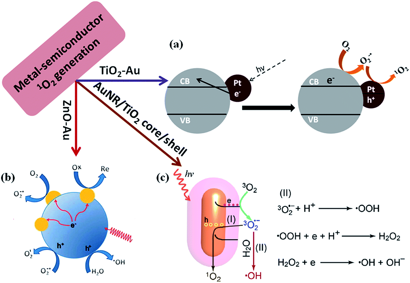 | ||
| Fig. 11 Scheme illustrations of the proposed mechanism for plasmon-enhanced 1O2 generation. (a) Au nanoparticle decorated on TiO2 for 1O2 generation, in which Au NPs enhanced the visible light photocatalytic efficiency by hot electron injection mechanism (b) proposed reaction mechanism for enhancement of 1O2 generation using ZnO–Au NP hybrid catalysts. Deposition of Au onto ZnO increases the charge carrier separation and transport efficiency in photoexcited ZnO nanoparticles. (c) Generation of singlet oxygen (1O2) through path (I) and hydroxyl radical ˙OH through path (II) by using Au NR/TiO2 core–shell nanostructure catalyst. Figures (a), (b) and (c) reproduced with permission from ref. 109, 111 and 112, respectively. | ||
4.4 Hot-electron-induced chemical transformations
Recent studies have shown that plasmonic nanostructures could be utilized to drive the chemical reactions through visible light excitation of their localised surface plasmon resonances.1,46,114–132 The LSPRs of plasmonic nanoparticles helps to concentrate the low intensity visible light and directs into adsorbed molecules to enhance the rate of chemical transformations in selective manner.46,114,116,121,127,131 The visible light excitation of surface plasmon resonances of plasmonic nanostructures leads to the increase of local heat as well as generation of hot electrons, which are the two main mechanisms proposed for the plasmon enhanced photochemical organic reactions. The excited surface plasmons decay via electron–phonon coupling followed lattice heating through phonon–phonon interactions. The local temperature on the surface of plasmonic nanostructures could be enhanced >500 °C under resonant excitation and this raise in temperature increases the rate of reaction.133 On the other hand, the hot electrons generated in the plasmonic nanostructures could be transferred to the adsorbed molecules that leads to the activation of the chemical bonds for chemical transformations.132In this section, we discuss the recent advances made toward plasmon-enhanced photocatalytic chemical reactions using various kinds of plasmonic nanostructures, as well as their reaction mechanisms. For example, Linic and co-workers have done pioneering work on chemical bond activation mechanism on plasmonic nanostructures through visible light excitation.1,131,132 They proposed a mechanistic model for the photo dissociation of oxygen molecule adsorbed on plasmonic metal nanoparticles (Fig. 12a).131,132 Upon visible light excitation, the hot electrons generated in the plasmonic nanoparticles (Ag nanocubes) transfers to the lowest unoccupied orbital (LUMO) of adsorbed oxygen molecule that leads to the formation of transient negative ion (TNI) O2− species (Fig. 12a). This process causes the elongation and weakening of O–O bond. Finally, the TNI relaxes by releasing an electron back to the metal and deposit vibrational energy on adsorbate molecule. If this acquired vibrational energy is sufficient enough to overcome the activation barrier, chemical transformations could takes place as shown in Fig. 12a. With multi-electron excitation, it is most likely that the lifetime of excited vibrational states (a few picoseconds) is significantly higher than the timescale of a vibration (a few femtoseconds), allowing the chemical reactions takes place (right panel of Fig. 12a).132 In a related work, they have also shown that silver nanocubes supported on α-Al2O3 particles could be used as photoactive catalytic to drive catalytic oxidation reactions such as ethylene CO oxidation, epoxidation, and NH3 oxidation at lower temperatures (using low-intensity visible light) than their conventional counterparts.131 Recent theoretical and experimental study by Avanesian et al.124 and Kale et al.128 suggested that it is possible to activate specific chemical bonds on metal surface by direct excitation of metal–adsorbate bonds through selective excitation wavelengths at optimum temperature. For example, by direct photoexcitation of Pt–CO hybridized electronic states allowing preferential CO oxidation in H2 rich stream using 5 nm Pt nanoparticles.128 Plasmon-enhanced photochemistry has been further applied for organic chemical transformations. For example, Li et al.118 demonstrated plasmon-enhanced selective oxidation of benzyl alcohol to benzaldehyde with O2 over Au@CeO2 nanoparticles of different morphologies under visible light illumination and the reaction mechanism is shown in Fig. 12b. The visible light excitation of Au@CeO2 composite nanoparticles in the presence of O2 leads to formation of highly reactive Ce-coordinated superoxide species (Ce(IV)–O–O˙) and they transform into cerium hydroperoxide upon reaction with benzyl alcohol. Finally, the dehydrogenated species gives another proton to cerium hydroperoxide to transform into benzaldehyde with H2O2 as side product.118 In general, such metal–semiconductor composites exhibit good catalytic activity for chemical transformations. However, the ratio between each component plays an important role in their efficiency and it should be optimised in order to achieve high efficiency. For instance, Jiang et al.115 studied the influence of Au NP loading on CeO2 nanorods (Au NPs were loaded by photodeposition) for photocatalytic oxidation of propylene under simulated sunlight and visible (>420 nm) light irradiation (Fig. 12d). They have found that the efficiency initially increased up to optimum loading of Au, however the efficiency decreased with further increase of Au loading due to increase of Au NPs size. The increase of the Au NPs size leads to saturation and decrease of exposed active sites for the adsorption of reactive species, resulting the decrease of catalytic efficiency.115 In addition to amount of plasmonic NPs loading, their support matrices such as CeO2, TiO2 and SiO2 also plays a key role in their catalytic efficiency. For instance, Halas and co-workers reported hot-electron-induced dissociation of H2 on Au NPs supported on SiO2 and they found that the catalytic efficiency was 2 orders of magnitude higher than that observed from Au NPs supported on TiO2.121 The rate of dissociation of H2 linearly depends on light intensity and the wavelength dependence resembles the extinction spectra of Au NPs, which further confirms the hot-electron-induced mechanism for the dissociation of H2 molecule. Very recently, Jiang et al.130 have reported plasmonic photocatalytic oxidation of benzyl alcohol using Au and Au–Pd NPs loaded TiO2 nanobelts as catalysts. In addition to the above discussed plasmonic photochemical conversions, hot-electron-induced conversion of aldehydes to esters,134 and ethyl chloride to ethane or butane129 have also been reported using supported plasmonic nanoparticles.
 | ||
| Fig. 12 (a) Scheme representation of molecular model for hot electron-driven chemical reactions on metals. The left panel shows that single electron excitation led to the deposition of vibrational energy into the adsorbate by accelerating the molecule along the potential energy surface of transient negative ion. If the vibrational energy is not sufficient to overcome the activation barrier, Ea, the adsorbate returns to the thermally equilibrated state. The right panel shows that the adsorbate is excited multiple times to overcome the activation barrier for chemical reactions to takes place. (b) Proposed reaction mechanism for plasmon induced selective oxidation of benzyl alcohol to benzaldehyde over the Au@CeO2 core–shell nanoparticle catalyst in the presence of O2 with visible light illumination. (c) Scheme showing plasmon-enhanced formic acid dehydrogenation on single Pd–Au nanorod. (d) Proposed reaction mechanism for aerobic oxidation of propylene on Au loaded CeO2 nanorods under solar irradiation. Figures (a), (b), (c), and (d) reproduced with permission from ref. 132, 118, 123 and 115, respectively. | ||
Besides the metal–semiconductor composite materials, pure-plasmonic nanoparticles have also been found as good catalysts for photocatalytic chemical reactions.122,123 For example, very recently Majima and co-workers reported a single particle study of plasmon-enhanced formic acid dehydrogenation using Au–Pd nanorods as photocatalysts, where Pd acts as catalytic site and Au acts as light absorber (Fig. 12c).123 Such particles exhibit efficient activity for formic acid dehydrogenation even well below room temperature (5 °C). One of the important findings from such single particle study is that only Pd on the tips of Au NRs can be affected for the occurrence of plasmon resonance energy transfer.123 Similarly such Au–Pd NRs could also be used as photocatalysts for plasmonic harvesting of light energy for Suzuki coupling reactions, as reported by Wang et al.122
4.5 Plasmon-enhanced photovoltaics
Photovoltaics is a process of converting solar light into direct electricity using semiconductor materials that shows photovoltaic response.135 During the last two decades, the research on photovoltaics has attracted great deal of attention due to their technological applications.136,137 They are expected to play a key role in solving the energy problems that our society would face in future. Great amount of research has been carried out to devise various types of photovoltaic systems for high power conversion efficiency. So far, most of the commercialized solar cells available in market are based on crystalline silicon solar cells. However, they are quite expensive due to high processing cost of crystalline silicon. Alternatively, significant amount of research has been carried out to fabricate thin film solar cells based on other type of semiconductor materials such as GaAs, metal chalcogenides and organic small molecules, as well as polymer semiconductors. But, one of the major challenges that scientists are trying to overcome is improving the efficiency of photovoltaic devices, as well as lowering the cost of production. Over the years, significant research efforts have been devoted to improve the efficiency of photovoltaic devices based on optimizing the band gap of semiconductors as well as device design.Recently, plasmonic nanoparticles have attracted considerable and increasing attention in the field of photovoltaics research to improve the efficiency of photovoltaic devices such as solar cells (quantum dot, polymer as well as dye sensitized) and light emitting devices.36,41–44,47,48,112,135–173 Plasmonic nanoparticles have the ability to guide and concentrate light at the nanometer scale.44,174 A review article by Atwater and Polman provided an overview of different design strategies to incorporate plasmonic nanostructures into solar cells in order to improve their efficiency through efficient light trapping.44 In general, there are three different approaches for the design of plasmonic nanostructures for efficient light coupling into solar cells, as shown in Fig. 13a.44 First, plasmonic nanoparticles could be used as light scatterers by placing them at the interface between two dielectrics, in which light scatters preferentially into dielectric medium with higher permittivity (Fig. 13a-I). The scattered light will most likely trapped inside solar cell photoactive medium as it reflects beyond critical angle of reflection. In addition, the effective path length could be significantly improved by placing a reflection mirror at the back of solar cell device, so that the incident solar light will passes through the active medium (semiconductor film) several times, resulting an increase in light absorption (Fig. 13a-I). Second, plasmonic nanostructures could be incorporated inside the semiconductor film to increase the absorption cross-section through near-field plasmonic absorption enhancement (Fig. 13a-II). The third approach is based on the excitation of surface plasmon polariton (SPP) modes at the metal/semiconductor interface using a corrugated metallic film on the back surface of a thin photovoltaic absorber layer (Fig. 13a-III). Such theoretical approaches have motivated researchers to make significant efforts for the development of plasmonic dye-sensitized,36,41,42,112,138,140,143,150,153,159,161,162,169,172,175 polymer47,48,138,139,147–150,155–157,160,162,165,176,177 and inorganic142,146,158,178 solar cells with improved efficiency. However, the observed improvement is very minimum and far reaching the theoretical enhancements. Moreover, there has been much controversy over the improvement of device performance by the incorporation of plasmonic nanoparticles in the active layer of organic solar cells, where plasmonic nanoparticles could quench the excitons generated in the active layer via electron transfer and result in the decrease of device efficiency.179 So, it is important to consider both light trapping and as well as quenching effects in the fabrication of plasmonic solar cells with improved efficiency. In this section, we will discuss various design strategies that have been implemented to reduce exciton quenching and at the same time enhance the light trapping behaviour for the fabrication of efficient plasmonic solar cells, with more emphasis on recent advances made toward this direction.
 | ||
| Fig. 13 (a) Schematic showing different design strategies for light trapping in solar cells. Light can be trapped via (I) multiple light scattering (I), (II) LSPR induced field enhancement, and (III) by the excitation of surface plasmon polaritons at the metal/semiconductor interface. (b) Schematic representation plasmonic bulk heterojunction (BHJ) solar cell, in which plasmonic NPs are embedded in PEDOT:PSS layer. The optical path length increased because of multiple and high-angle scattering light scattering in active layer in the presence of plasmonic NPs (left). In addition to light scattering, electric field enhancement also contributes to the enhanced efficiency (right). Schematic representation showing the exciton–plasmon coupling led to enhancement in rate of exciton dissociation, thereby reducing exciton recombination. (c) Schematic illustration of CdSe NPs on Al2O3-coated Ag NPs surface. The distance between Ag NP film and CdSe NPs are tuned by varying the thickness of the Al2O3 layer. Optical properties (fluorescence and fluorescence life time) of QDs as a function of distance between QDs and Ag film are recorded to investigate the distance dependent plasmonic effect of Ag NPs. Figures (a), (b) and (c) reproduced with permission from ref. 44, 148 and 178, respectively. | ||
The recent reports on different types of plasmonic solar cells fabricated using various kinds of plasmonic nanostructures are summarized in Table 1. Plasmonic nanoparticles could enhance or detract the efficiency of solar cells via enhanced absorption and exciton quenching, respectively. One of the most important factor that should be considered in the design of plasmonic solar cells is the distance between quantum dot (QD) layer and plasmonic NPs. Recently Jin et al.178 studied plasmon enhanced light absorption in CdSe QDs sensitized on silver (Ag) nanoparticle (NP) films as a function of interparticle distance between Ag and CdSe, where the distance between two films were controlled by Al2O3 (Fig. 13c). When the separation distance was ∼2 nm, the fluorescence intensity of QDs was largely quenched, however maximum enhancement (24-fold) was observed when the separation distance was ∼5 nm. In addition, excitation wavelength dependent enhancement studies and fluorescence lifetime measurements suggests that the observed enhancement was mainly due to the enhancement in photoabsorption in CdSe QDs by the plasmon of Ag NPs.178
| Solar cell type | Photoactive medium | Plasmonic nanostructure | Main result (efficiency improvement) | Ref. |
|---|---|---|---|---|
| Bulk heterojunction (BHJ) polymer solar cell | Polymer poly(indacenodithieno[3,2-b]thiophene-difluoro-benzothiadiazole) (PIDTT-DFBT) and [6,6]-phenyl-C71-butyric acid methyl ester (PC71BM) | Silver nanoprisms | Power conversion efficiency (PEC) increased around 16–18% | 176 |
| BHJ polymer solar cell | Polythieno[3,4-b]thiophene/benzodithiophene (PTB7) and PC71BM | Au@polystyrene core–shell nanoparticles | PEC increased from 7.6% to 8.4% | 181 |
| BHJ polymer solar cell | Poly[N-9-hepta-decanyl-2,7-carbazolealt-5,5-(4,7-di-2-thienyl-2,1,3-benzothiadiazole)] (PCDTBT):[6,6]-phenyl C71-butyric acid methyl ester (PC70BM) | Au@Ag core–shell nanocubes and Au NPs | PCE of 9.2% was achieved. Solar cells with the embedded Au@Ag NCs showed 2.2-fold absorption enhancement at wavelengths of 450–700 nm compared to Au NPs | 141 |
| BHJ polymer solar cell | Polythieno[3,4-b]-thiophene/benzodithiophene (PTB7) and PC70BM | Mixture of Au & Ag NPs | PEC enhanced by 20% | 177 |
| Inverted BHJ polymer solar cell | Poly(3-hexylthiophene):[6,6]-phenyl-C61-butyric acid methyl ester (P3HT:PCBM) | Au & ZnO NPs | 5% enhancement was achieved due to increased fill factor rather than photocurrent | 160 |
| BHJ polymer solar cell | P3HT:PCBM | Ag NPs and Ag nanoprisms | PCE enhanced by 19.44% | 150 |
| BHJ polymer solar cell | P3HT:PCBM | Au NPs | PCE enhanced by 16% | 156 |
| BHJ polymer solar cell | PTB7:PC70BM | Coupled Au NPs | PCE improved from 8.29 to 9.48% | 173 |
| BHJ polymer solar cell | P3HT:PC61BM | Au–Ag alloy nanoparticles | PCE enhanced by 31% using 1% Au11 Ag89 alloy NPs | 149 |
| Inverted BHJ polymer solar cell | ZnO/P3HT:PCBM | Spray-deposited Au nanoparticles | PCE enhanced by 17–26% | 165 |
| C–silicon/organic polymer hybrid solar cell | C–Si/PEDOT:PSS | Au/Ag bimetallic multispiked nanoparticles | PCE improved from 6.72% to 7.70% | 139 |
| BHJ polymer solar cell | P3HT:PCBM | Au octahedral NPs | PCE improved from 3.57% to 4.24% | 148 |
| Panchromatic dye-sensitized solar cell (DSSC) | N719 dye | Multiple-core–shell structured TiO2–Au–TiO2, Au–TiO2 and Ag–TiO2 NPs | PCE improved from 8.3% to 10.8% | 162 |
| DSSC | 9,10-Anthracenediyl-bis(methylene)dimalonic acid (ABDA) | (Gold core)/(titania shell) nanostructures | PCE enhanced by 13.3% | 112 |
| DSSC | N719 dye | Au@SiO2 nanocubes | 34% improvement of DSSC performance | 41 |
| DSSC | N719 dye | Au@SiO2 NPs | PCE improved from 9.3% to 10.2% | 143 |
| DSSC | N719 dye | TiO2 nanowires–Au NPs composite | PCE improved from 6.25% to 9.37% | 140 |
| Plasmonic-quantum dot (QD) solar cell | PbS semiconductor nanocrystals | 5 nm Au NPs | PCE improved from 4.0% (PbS-only) to 4.2% (Au, PbS) | 146 |
| Plasmonic-quantum dot (QD) solar cell | HgTe QDs | ZnO–Au NRs | Average Jsc values were increased by more than 80 and 240% in the devices with Au nanorods embedded below 7.5 and 4.5 nm ZnO layers, respectively | 142 |
To date, most of the reported high performance organic solar cells are based on bulk heterojunction concept, where a blend of poly(3-hexylthiophene) (P3HT) and [6,6]-phenyl-C61-butyric acid methyl ester (PCBM) acts as active medium (Fig. 13b).180 Recently, significant progress has been made to improve the efficiency of P3HT–PCBM solar cells by incorporating metal nanostructures, where both enhancement and detraction in efficiency have been reported.43,47,48,138,148–150,156,165,173,177,179 In general, plasmonic nanoparticles have often been incorporated in anodic buffer layer (PEDOT:PSS hole conducting layer) in order to avoid direct contact with active layer (P3HT:PCBM) and the device structure is shown in Fig. 13b. For example, Wu et al.148 have shed some light on coupling process between the electromagnetic field and the photo generated excitons (exciton–plasmon coupling process) within the photoactive blend (P3HT:PCBM) via time-resolved photoluminescence (Fig. 13b). They observed an increase in the fluorescence intensity and reduced lifetime of photogenerated excitons in the active blend, which they attributed to the increase of light absorption induced by surface plasmon resonance followed by charge transfer from photoexcited polymer blend to plasmonic NPs, thereby, decreasing the rate of exciton recombination. As a result, both the photocurrent and fill factor of solar cell device was significantly enhanced and they observed a power conversion efficiency of 4.24% in the presence of Au NPs, compared to a value of 3.57% without Au NPs.148 Most of the reported studies showed an improvement in the performance of solar cells by the incorporation of plasmonic nanoparticles in PEDOT:PSS layer. However, there is still a debate on the incorporation of plasmonic nanostructures in the active layer of solar cells, where both enhancement and decrease of performance has been observed. For instance, Topp et al.179 have reported a study on influence of the incorporation of Au NPs into polymer/fullerene solar cells and a decrease of the device performance was observed in all the cases irrespective of the type of ligands that were capped to the NPs or the weight percentage of NPs incorporated. The decrease of efficiency was attributed to efficient quenching of excited states in the polymer phase and as well as the segregation of Au at the interface between the active layer and the Al contact. So, the design of plasmonic solar cells should be in such a ways that plasmonic NPs do not quench the excitons. Toward this direction, Yao et al.176 demonstrated a general approach to enhance the efficiency of polymer solar cells using plasmonic nanostructures (Fig. 14a). The solar cell design is based on the deposition of photoactive layer in between dual layers of Ag nanoprisms, in which the light can be well trapped in the active layer with multiple reflections between two plasmonic layers, thereby increasing the absorption correction (Fig. 14a). The solar cell efficiency was found to be higher in the case of dual Ag layers with a maximum improvement of 18% power conversion efficiency (PCE) compared to that of device without Ag nanoprisms. In addition, transient absorption studies further confirms that the observed enhancement is consistent with enhanced optical absorption. In a related work, Au@Ag core–shell nanocubes were incorporated into PEDOT:PSS layer of bulk heterojunction (BHJ) polymer solar cell and the power conversion efficiency was improved by 16–18% depending on the type of polymer used in the active layer (Fig. 14b).141 In general Ag NPs exhibit higher extinction over Au NPs and thus expected to give higher enhancements. It was observed that Au@Ag core–shell NPs showed 2.2-fold higher external quantum efficiency enhancement compared to the Au NPs devices due to enhanced scattering efficiency, which was further supported by theoretical calculations and detailed optical measurements.141 In order to understand the origin of enhanced efficiency in plasmonic solar cells, Liu et al.47 have studied the influence of a single silver nanowire (NW) on the charge carriers in BHJ polymer solar cells through spatially resolved optical spectroscopy, and correlate to electrical device characterization (Fig. 14c). They have observed a maximum enhancement of 36% when the transverse plasmon mode of Ag NW is activated, suggesting higher absorbance due to higher light scattering perpendicular to the NW long axis.47 In order to avoid the direct contact of plasmonic NPs with photoactive layer, dielectric coatings have also been applied to plasmonic nanoparticles before they incorporate into solar cell devices. For instance, Au@polystyrene (PS) core–shell nanoparticles have been incorporated into organic optoelectronic devices (organic light emitting diodes (OLED) and solar cells), reported by Kim et al.181 The current efficiency of OLED device was enhanced by 42% and the power conversion efficiency was increased from 7.6% to 8.4% in PTB7:PC71BM solar cell with the incorporation of Au@PS NPs (Fig. 14d).
 | ||
| Fig. 14 (a) Schematic illustration of single and dual interfacial layer strategy for the fabrication of plasmonic bulk heterojunction (BHJ) solar cell device using PIDTT-DFBT:PC71BM as photoactive material and corresponding SEM images of Ag nanoprisms that are incorporated into device. The device with multiple layers of Ag nanoprisms shows higher photoconversion efficiency due to multiple light scattering in the photoactive medium. (b) Schematic representation of plasmonic BHJ solar cell by the incorporation of Au@Ag core–shell NPs in PEDOT:PSS layer. (c) Schematic illustration of plasmonic organic solar cell with single Ag nanowire (NW). The figure on the right side shows the plot of polarization dependent micro/localized I–V characteristics (inset shows the optical micrograph of the single NW where the pump polarization is perpendicular (90° of polarization) and parallel (0° of polarization) to the long axis of the Ag NW). (d) TEM image of Au@polystyrene core–shell NPs and the schematic representation of photovoltaic devices (OLED and OPV) fabricated by the incorporation of Au@PS NPs in PEDOT:PSS layer. Figures (a), (b), (c), and (d) reproduced with permission from ref. 176, 141, 47 and 181, respectively. | ||
Besides, plasmonic NPs have also been incorporated into dye-sensitized solar cells (DSSC) to improve their power conversion efficiency. For example, Kamat and co-workers reported that the efficiency of an N719 dye-sensitized solar cell (9.3%) increased to 10.2% and 9.8% with incorporation of 0.7% Au@SiO2 and 0.7% Au@TiO2 NPs, respectively.143 The obtained results were attributed to the surface plasmon resonance enhanced photocurrent, while the charging effects lead to an increase in photovoltage. Very recently, Bardhan and co-workers reported 34% improvement in the PCE of dye-sensitized solar cells using Au@SiO2 nanocubes (Fig. 15).41 They have also found that there is a monotonic decrease in PEC at very high nanocube concentration. The observed enhancement was attributed to light amplification by field enhancement, which was further confirmed by finite difference time domain simulations. Besides, photonic crystal coupled plasmonic nanoparticle arrays enhanced the PCE of DSSC by 41% compared to control, reported by Li et al.169
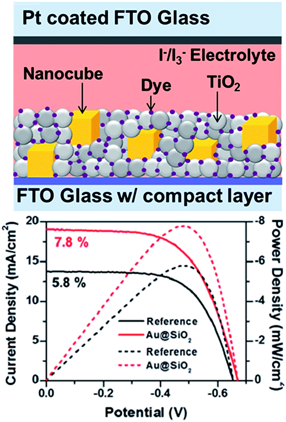 | ||
| Fig. 15 Schematic illustration of plasmonic DSSC device structure, showing nanocubes embedded within the N719-sensitized mesoporous TiO2 layer with I−/I3− liquid electrolyte (d) device performance: current density (solid lines) and power density (dashed lines) curves of the DSSCs with and without (reference) Au@SiO2 core–shell nanocubes. Figure reproduced with permission from ref. 41. | ||
Furthermore, plasmonic nanostructures have been incorporated into graphene based photovoltaic devises to improve their efficiency through plasmonic field-enhancement.163,182 For instance, Halas and co-workers have reported a graphene–antenna sandwich photodetector based on gold nanostructures (antenna) sandwiched between two graphene monolayers, as shown in Fig. 16a–d.163 They have found that the efficiency of photodetector that converts visible and near-infrared photons into electrons was enhanced by 800% in the presence of plasmonic nanostructures (Fig. 16d). The enhancement was attributed to direct plasmon-enhanced excitation of intrinsic graphene electrons, as well as due to hot electron transfer from antenna to graphene. Antisymmetric photocurrent response observed in the line scan measurement between source and drain further confirms the enhancement was due to field enhancement (Fig. 16d). Similarly, plasmonic nanostructures have also been used to enhance the optical properties of another two dimensional material ‘monolayer molybdenum disulfide’ (MoS2).183 MoS2 is a promising two-dimensional nanomaterial for optoelectronics due to its direct band gap and broad absorption properties. It was found that the partial coverage of Au nanoshells on MoS2 monolayer lead to enhancements of photoluminescence and photocurrent by two-fold and three-fold, respectively (Fig. 16e).183 In addition, plasmonic nanostructures alone could be used for photodetection based on the hot electron induced photocurrent (Fig. 16f). For instance, Sobhani et al. have reported a grating-based hot electron photodetector device that shows high photocurrent responsivity and narrower spectral response over other nanoantenna-based devices (Fig. 16f). Moreover, the spectral and photocurrent response could be tuned by varying the inter-slit distance and grating thickness.184
 | ||
| Fig. 16 (a) Schematic illustration of graphene–antenna sandwich photodetector, showing single gold heptamer sandwiched between two monolayer graphene sheets. VG is the gate voltage used to electrostatically dope the graphene on Si/SiO2 substrate. (b) Optical microscopy image of the device before (left) and after (right) deposition of the second graphene layer. Inset: Raman mapping (G mode) of device areas 1–5 using 785 nm laser. (c) SEM of the device before and after deposition of the second graphene layer. (d) Line scan photocurrent measurements with and without plasmonic nanostructures, showing enhanced photocurrent as well as antisymmetric photocurrent responses from the different regions of the device corresponding to specific plasmonic antenna geometries. (f) Schematic representation of grating-Schottky photodetector oriented transverse to the laser polarization, showing a gold grating on an n-type silicon substrate, which were separated with a 2 nm Ti adhesion layer. Polarization of the incident laser and its k vector are represented in yellow and green arrows, respectively. Figures (a–d), (e) and (f) reproduced with permission from ref. 163, 183 and 184, respectively. | ||
5. Summary and future directions
Plasmonic nanostructures have been playing a significant role in the development of visible light photocatalysts to harvest solar energy for various applications. Integration of plasmonic nanostructures with semiconductor photoactive materials have opened doors for new type of photocatalytic systems for efficient solar light harvesting. In this review, we introduced different strategies such as direct growth of plasmonic nanocrystals on semiconductor surface, coating of semiconductor shells on plasmonic nanocrystals, templated synthesis and photo induced deposition methods for the synthesis of metal–semiconductor hybrid nanostructures. In addition, we summarized recent progress on plasmon-enhanced light harvesting using various plasmonic nanostructures and their applications for enhanced-photocatalytic degradation of organic pollutants, hydrogen generation, chemical transformations and photovoltaics. Although significant of progress has been made during the last few years, but still many challenges to be addressed to explore the use of plasmonic nanostructures for enhanced light harvesting with full potential.For example, many of the photocatalytic systems have been tested for the degradation of standard organic dyes. However, there are various kinds of other pollutants that can affect people's health. It is important to test photocatalytic ability of various catalysts towards real pollutants. In addition, the efficiency of hydrogen production by photocatalytic water splitting using plasmonic catalysts is very low and it is far from commercialization. So far most of the research has been mainly focused on understanding different systems for photocatalytic water splitting and it is still in preliminary stage. It is very important to accelerate the research toward the large scale production of H2 generation based on current understanding. Most of the prepared plasmonic photocatalysts are based on Au nanostructures, however the cost of photocatalytic systems has to be reduced as Au is very expensive. Besides, the maximum enhancement of visible light photocatalytic activity is at the SPR maximum, which was also proved by wavelength dependent photocurrent measurements. So, it would be interesting to fabricate plasmonic–semiconductors with broad absorption to further enhance the efficiency. Another important challenge to be addressed in future is the stability and recyclability of photocatalysts.
Moreover, the mechanism behind plasmon enhanced chemical transformations has not been well investigated due to experimental limitations. It is not very clear that the chemical transformation occurs due to hot electron transfer from metal to adsorbate or heat generated by plasmonic nanocrystals upon interacting with light. Significant efforts have been devoted to increase the power conversion efficiency of photovoltaics by incorporation of various plasmonic nanostructures. However, the enhancement is still very low and far behind the theoretically predicted enhancements. Energy efficiency design strategies are key to the development of plasmonic–photovoltaic systems with enhanced efficiency.
Recent research progress on exploring the metal–semiconductors based photocatalytic systems suggests that the integration of plasmonic nanostructures with semiconductors is a powerful strategy to exploit visible light driven photocatalysts for solar energy conversion. We believe that the exploration of above mentioned challenges will lead to rapid progress of field toward real world applications through efficient solar light harvesting.
Acknowledgements
This work is supported by the AcRF Tier 1 grant (R-143-000-533-112), the SPORE program (COY-15-EWI-RCFSA/N197-1) under National Research Foundation and the Economic Development Board of Singapore, by the Spanish Ministry of Economy and Competitivity (MAT2013-45168-R) and by the Xunta de Galicia/FEDER (GPC2013-006; INBIOMED-FEDER “Unhamaneira de facer Europa”).Notes and references
- S. Linic, P. Christopher and D. B. Ingram, Nat. Mater., 2011, 10, 911–921 CrossRef CAS PubMed.
- D. Ravelli, M. Fagnoni and A. Albini, Chem. Soc. Rev., 2013, 42, 97–113 RSC.
- X. Lang, X. Chen and J. Zhao, Chem. Soc. Rev., 2014, 43, 473–486 RSC.
- M. G. Walter, E. L. Warren, J. R. McKone, S. W. Boettcher, Q. Mi, E. A. Santori and N. S. Lewis, Chem. Rev., 2010, 110, 6446–6473 CrossRef CAS PubMed.
- S. Banerjee, S. C. Pillai, P. Falaras, K. E. O'Shea, J. A. Byrne and D. D. Dionysiou, J. Phys. Chem. Lett., 2014, 5, 2543–2554 CrossRef CAS.
- O. Diaz-Morales, F. Calle-Vallejo, C. de Munck and M. T. M. Koper, Chem. Sci., 2013, 4, 2334–2343 RSC.
- R. Jiang, B. Li, C. Fang and J. Wang, Adv. Mater., 2014, 26, 5274–5309 CrossRef CAS PubMed.
- X. Zhang, Y. Liu, S.-T. Lee, S. Yang and Z. Kang, Energy Environ. Sci., 2014, 7, 1409–1419 CAS.
- P. V. R. K. Ramacharyulu, J. Praveen kumar, G. K. Prasad and A. R. Srivastava, RSC Adv., 2015, 5, 1309–1314 RSC.
- V. Scuderi, G. Impellizzeri, L. Romano, M. Scuderi, M. V. Brundo, K. Bergum, M. Zimbone, R. Sanz, M. A. Buccheri, F. Simone, G. Nicotra, B. G. Svensson, M. G. Grimaldi and V. Privitera, Nanoscale, 2014, 6, 11189–11195 RSC.
- A. Primo, A. Corma and H. Garcia, Phys. Chem. Chem. Phys., 2011, 13, 886–910 RSC.
- N. Zhang, S. Liu and Y. J. Xu, Nanoscale, 2012, 4, 2227–2238 RSC.
- P. D. Cozzoli, R. Comparelli, E. Fanizza, M. L. Curri, A. Agostiano and D. Laub, J. Am. Chem. Soc., 2004, 126, 3868–3879 CrossRef CAS PubMed.
- A. P. Alivisatos, Science, 1996, 271, 933–937 CAS.
- S. I. Shah, W. Li, C.-P. Huang, O. Jung and C. Ni, Proc. Natl. Acad. Sci. U. S. A., 2002, 99, 6482–6486 CrossRef CAS PubMed.
- M. R. Hoffmann, S. T. Martin, W. Choi and D. W. Bahnemann, Chem. Rev., 1995, 95, 69–96 CrossRef CAS.
- A. L. Linsebigler, G. Lu and J. T. Yates, Chem. Rev., 1995, 95, 735–758 CrossRef CAS.
- X. Chen and S. S. Mao, Chem. Rev., 2007, 107, 2891–2959 CrossRef CAS PubMed.
- A. Fujishima and K. Honda, Nature, 1972, 238, 37–38 CrossRef CAS.
- D. B. Ingram and S. Linic, J. Am. Chem. Soc., 2011, 133, 5202–5205 CrossRef CAS PubMed.
- M. Gratzel, Nature, 2001, 414, 338–344 CrossRef CAS PubMed.
- Y. Liu, J. R. Jennings, S. M. Zakeeruddin, M. Gratzel and Q. Wang, J. Am. Chem. Soc., 2013, 135, 3939–3952 CrossRef CAS PubMed.
- Y. Tian and T. Tatsuma, J. Am. Chem. Soc., 2005, 127, 7632–7637 CrossRef CAS PubMed.
- A. Takai and P. V. Kamat, ACS Nano, 2011, 5, 7369–7376 CrossRef CAS PubMed.
- M. Ni, M. K. H. Leung, D. Y. C. Leung and K. Sumathy, Renewable Sustainable Energy Rev., 2007, 11, 401–425 CrossRef CAS PubMed.
- S. U. M. Khan, M. Al-Shahry and W. B. Ingler, Science, 2002, 297, 2243–2245 CrossRef CAS PubMed.
- J. B. Varley, A. Janotti and C. G. Van de Walle, Adv. Mater., 2011, 23, 2343–2347 CrossRef CAS PubMed.
- W. J. Youngblood, S.-H. A. Lee, K. Maeda and T. E. Mallouk, Acc. Chem. Res., 2009, 42, 1966–1973 CrossRef CAS PubMed.
- Y. Tian and T. Tatsuma, Chem. Commun., 2004, 1810–1811 RSC.
- A. Tanaka, S. Sakaguchi, K. Hashimoto and H. Kominami, ACS Catal., 2012, 3, 79–85 CrossRef.
- T. Hirakawa and P. V. Kamat, J. Am. Chem. Soc., 2005, 127, 3928–3934 CrossRef CAS PubMed.
- N. Zhou, L. Polavarapu, N. Gao, Y. Pan, P. Yuan, Q. Wang and Q. H. Xu, Nanoscale, 2013, 5, 4236–4241 RSC.
- Y. Pan, S. Deng, L. Polavarapu, N. Gao, P. Yuan, C. H. Sow and Q.-H. Xu, Langmuir, 2012, 28, 12304–12310 CrossRef CAS PubMed.
- K. L. Kelly, E. Coronado, L. L. Zhao and G. C. Schatz, J. Phys. Chem. B, 2002, 107, 668–677 CrossRef.
- M. Rycenga, C. M. Cobley, J. Zeng, W. Li, C. H. Moran, Q. Zhang, D. Qin and Y. Xia, Chem. Rev., 2011, 111, 3669–3712 CrossRef CAS PubMed.
- C.-H. Chou and F.-C. Chen, Nanoscale, 2014, 6, 8444–8458 RSC.
- L. M. Liz-Marzán, Langmuir, 2005, 22, 32–41 CrossRef PubMed.
- C. Noguez, J. Phys. Chem. C, 2007, 111, 3806–3819 CAS.
- L. Polavarapu, J. Perez-Juste, Q.-H. Xu and L. M. Liz-Marzan, J. Mater. Chem. C, 2014, 2, 7460–7476 RSC.
- Z. Guan, L. Polavarapu and Q.-H. Xu, Langmuir, 2010, 26, 18020–18023 CrossRef CAS PubMed.
- H. F. Zarick, O. Hurd, J. A. Webb, C. Hungerford, W. R. Erwin and R. Bardhan, ACS Photonics, 2014, 1, 806–811 CrossRef CAS.
- S. D. Standridge, G. C. Schatz and J. T. Hupp, J. Am. Chem. Soc., 2009, 131, 8407–8409 CrossRef CAS PubMed.
- S. V. Boriskina, H. Ghasemi and G. Chen, Mater. Today, 2013, 16, 375–386 CrossRef CAS PubMed.
- H. A. Atwater and A. Polman, Nat. Mater., 2010, 9, 205–213 CrossRef CAS PubMed.
- L. Polavarapu and L. M. Liz-Marzan, Phys. Chem. Chem. Phys., 2013, 15, 5288–5300 RSC.
- M. Xiao, R. Jiang, F. Wang, C. Fang, J. Wang and J. C. Yu, J. Mater. Chem. A, 2013, 1, 5790–5805 CAS.
- X. Liu, B. Wu, Q. Zhang, J. N. Yip, G. Yu, Q. Xiong, N. Mathews and T. C. Sum, ACS Nano, 2014, 8, 10101–10110 CrossRef CAS PubMed.
- B. Wu, X. Wu, C. Guan, K. Fai Tai, E. K. L. Yeow, H. Jin Fan, N. Mathews and T. C. Sum, Nat. Commun., 2013, 4, 2004 Search PubMed.
- T. Hirakawa and P. V. Kamat, Langmuir, 2004, 20, 5645–5647 CrossRef CAS.
- M. Jakob, H. Levanon and P. V. Kamat, Nano Lett., 2003, 3, 353–358 CrossRef CAS.
- V. Subramanian, E. E. Wolf and P. V. Kamat, J. Am. Chem. Soc., 2004, 126, 4943–4950 CrossRef CAS PubMed.
- P. Sangpour, F. Hashemi and A. Z. Moshfegh, J. Phys. Chem. C, 2010, 114, 13955–13961 CAS.
- X.-F. Wu, H.-Y. Song, J.-M. Yoon, Y.-T. Yu and Y.-F. Chen, Langmuir, 2009, 25, 6438–6447 CrossRef CAS PubMed.
- X.-F. Wu, Y.-F. Chen, J.-M. Yoon and Y.-T. Yu, Mater. Lett., 2010, 64, 2208–2210 CrossRef CAS PubMed.
- Z. W. Seh, S. Liu, M. Low, S.-Y. Zhang, Z. Liu, A. Mlayah and M.-Y. Han, Adv. Mater., 2012, 24, 2310–2314 CrossRef CAS PubMed.
- K. Awazu, M. Fujimaki, C. Rockstuhl, J. Tominaga, H. Murakami, Y. Ohki, N. Yoshida and T. Watanabe, J. Am. Chem. Soc., 2008, 130, 1676–1680 CrossRef CAS PubMed.
- S. K. Cushing, J. Li, F. Meng, T. R. Senty, S. Suri, M. Zhi, M. Li, A. D. Bristow and N. Wu, J. Am. Chem. Soc., 2012, 134, 15033–15041 CrossRef CAS PubMed.
- X. Zhang, Y. Zhu, X. Yang, S. Wang, J. Shen, B. Lin and C. Li, Nanoscale, 2013, 5, 3359–3366 RSC.
- A. Furube, L. Du, K. Hara, R. Katoh and M. Tachiya, J. Am. Chem. Soc., 2007, 129, 14852–14853 CrossRef CAS PubMed.
- L. Du, A. Furube, K. Hara, R. Katoh and M. Tachiya, J. Photochem. Photobiol., C, 2013, 15, 21–30 CrossRef CAS PubMed.
- P. Christopher, D. B. Ingram and S. Linic, J. Phys. Chem. C, 2010, 114, 9173–9177 CAS.
- M. K. Kumar, S. Krishnamoorthy, L. K. Tan, S. Y. Chiam, S. Tripathy and H. Gao, ACS Catal., 2011, 1, 300–308 CrossRef CAS.
- J. Lee, T. Javed, T. Skeini, A. O. Govorov, G. W. Bryant and N. A. Kotov, Angew. Chem., Int. Ed., 2006, 45, 4819–4823 CrossRef CAS PubMed.
- C. Burda, X. Chen, R. Narayanan and M. A. El-Sayed, Chem. Rev., 2005, 105, 1025–1102 CrossRef CAS PubMed.
- S. T. Kochuveedu, Y. H. Jang and D. H. Kim, Chem. Soc. Rev., 2013, 42, 8467–8493 RSC.
- J. Kimling, M. Maier, B. Okenve, V. Kotaidis, H. Ballot and A. Plech, J. Phys. Chem. B, 2006, 110, 15700–15707 CrossRef CAS PubMed.
- M. Brust, M. Walker, D. Bethell, D. J. Schiffrin and R. Whyman, Chem. Commun., 1994, 801–802 RSC.
- Z. Bian, J. Zhu, F. Cao, Y. Lu and H. Li, Chem. Commun., 2009, 3789–3791 RSC.
- C. G. Silva, R. Juarez, T. Marino, R. Molinari and H. Garcia, J. Am. Chem. Soc., 2011, 133, 595–602 CrossRef PubMed.
- S. T. Kochuveedu, D.-P. Kim and D. H. Kim, J. Phys. Chem. C, 2011, 116, 2500–2506 Search PubMed.
- L. Zhang, D. A. Blom and H. Wang, Chem. Mater., 2011, 23, 4587–4598 CrossRef CAS.
- L. Zhang, H. Jing, G. Boisvert, J. Z. He and H. Wang, ACS Nano, 2012, 6, 3514–3527 CrossRef CAS PubMed.
- Y. Zheng, C. Chen, Y. Zhan, X. Lin, Q. Zheng, K. Wei and J. Zhu, J. Phys. Chem. C, 2008, 112, 10773–10777 CAS.
- D. D. Lekeufack, A. Brioude, A. Mouti, J. G. Alauzun, P. Stadelmann, A. W. Coleman and P. Miele, Chem. Commun., 2010, 46, 4544–4546 RSC.
- I. Pastoriza-Santos, D. S. Koktysh, A. A. Mamedov, M. Giersig, N. A. Kotov and L. M. Liz-Marzán, Langmuir, 2000, 16, 2731–2735 CrossRef CAS.
- K. S. Mayya, D. I. Gittins and F. Caruso, Chem. Mater., 2001, 13, 3833–3836 CrossRef CAS.
- Z. W. Seh, S. Liu, S. Y. Zhang, M. S. Bharathi, H. Ramanarayan, M. Low, K. W. Shah, Y. W. Zhang and M. Y. Han, Angew. Chem., Int. Ed., 2011, 50, 10140–10143 CrossRef CAS PubMed.
- Z. W. Seh, S. Liu, S. Y. Zhang, K. W. Shah and M. Y. Han, Chem. Commun., 2011, 47, 6689–6691 RSC.
- B. Nikoobakht and M. A. El-Sayed, Chem. Mater., 2003, 15, 1957–1962 CrossRef CAS.
- N. Meir, I. Jen-La Plante, K. Flomin, E. Chockler, B. Moshofsky, M. Diab, M. Volokh and T. Mokari, J. Mater. Chem. A, 2013, 1, 1763–1769 CAS.
- W.-C. Wang, L.-M. Lyu and M. H. Huang, Chem. Mater., 2011, 23, 2677–2684 CrossRef CAS.
- H. Jing, N. Large, Q. Zhang and H. Wang, J. Phys. Chem. C, 2014, 118, 19948–19963 CAS.
- B. Kraentler and A. J. Bard, J. Am. Chem. Soc., 1978, 100, 4317–4318 CrossRef.
- W. W. Dunn, Y. Aikawa and A. J. Bard, J. Am. Chem. Soc., 1981, 103, 6893–6897 CrossRef CAS.
- K. Kimura, S.-i. Naya, Y. Jin-nouchi and H. Tada, J. Phys. Chem. C, 2012, 116, 7111–7117 CAS.
- L. Carbone, A. Jakab, Y. Khalavka and C. Sönnichsen, Nano Lett., 2009, 9, 3710–3714 CrossRef CAS PubMed.
- X. Li, X. Fu and H. Yang, Phys. Chem. Chem. Phys., 2011, 13, 2809–2814 RSC.
- Q. Zhang, D. Q. Lima, I. Lee, F. Zaera, M. Chi and Y. Yin, Angew. Chem., Int. Ed., 2011, 50, 7088–7092 CrossRef CAS PubMed.
- Z. Jin, F. Wang, F. Wang, J. Wang, J. C. Yu and J. Wang, Adv. Funct. Mater., 2013, 23, 2137–2144 CrossRef CAS.
- L. Shao, Q. Ruan, R. Jiang and J. Wang, Small, 2014, 10, 802–811 CrossRef CAS PubMed.
- J. C. Yu, J. Yu, W. Ho and L. Zhang, Chem. Commun., 2001, 1942–1943 RSC.
- T.-T. Yang, W.-T. Chen, Y.-J. Hsu, K.-H. Wei, T.-Y. Lin and T.-W. Lin, J. Phys. Chem. C, 2010, 114, 11414–11420 CAS.
- L. He, L. Li, T. Wang, H. Gao, G. Li, X. Wu, Z. Su and C. Wang, Dalton Trans., 2014, 16981–16985 RSC.
- S. C. Warren and E. Thimsen, Energy Environ. Sci., 2012, 5, 5133–5146 CAS.
- K. Maeda and K. Domen, J. Phys. Chem. Lett., 2010, 1, 2655–2661 CrossRef CAS.
- F. E. Osterloh, Chem. Mater., 2007, 20, 35–54 CrossRef.
- K. Maeda, A. Xiong, T. Yoshinaga, T. Ikeda, N. Sakamoto, T. Hisatomi, M. Takashima, D. Lu, M. Kanehara, T. Setoyama, T. Teranishi and K. Domen, Angew. Chem., Int. Ed., 2010, 49, 4096–4099 CrossRef CAS PubMed.
- F. Su, T. Wang, R. Lv, J. Zhang, P. Zhang, J. Lu and J. Gong, Nanoscale, 2013, 5, 9001–9009 RSC.
- Z. Liu, W. Hou, P. Pavaskar, M. Aykol and S. B. Cronin, Nano Lett., 2011, 11, 1111–1116 CrossRef CAS PubMed.
- F. Le, D. W. Brandl, Y. A. Urzhumov, H. Wang, J. Kundu, N. J. Halas, J. Aizpurua and P. Nordlander, ACS Nano, 2008, 2, 707–718 CrossRef CAS PubMed.
- S. Zou and G. C. Schatz, Chem. Phys. Lett., 2005, 403, 62–67 CrossRef CAS PubMed.
- X. Chen, S. Shen, L. Guo and S. S. Mao, Chem. Rev., 2010, 110, 6503–6570 CrossRef CAS PubMed.
- J. P. Celli, B. Q. Spring, I. Rizvi, C. L. Evans, K. S. Samkoe, S. Verma, B. W. Pogue and T. Hasan, Chem. Rev., 2010, 110, 2795–2838 CrossRef CAS PubMed.
- C. Xing, Q. Xu, H. Tang, L. Liu and S. Wang, J. Am. Chem. Soc., 2009, 131, 13117–13124 CrossRef CAS PubMed.
- A. Ormond and H. Freeman, Materials, 2013, 6, 817–840 CrossRef CAS PubMed.
- Y. Nosaka, T. Daimon, A. Y. Nosaka and Y. Murakami, Phys. Chem. Chem. Phys., 2004, 6, 2917–2918 RSC.
- T. Daimon and Y. Nosaka, J. Phys. Chem. C, 2007, 111, 4420–4424 CAS.
- M. Buchalska, G. Kras, M. Oszajca, W. Łasocha and W. Macyk, J. Photochem. Photobiol., A, 2010, 213, 158–163 CrossRef CAS PubMed.
- X. Hu, H. Ji and L. Wu, RSC Adv., 2012, 2, 12378–12383 RSC.
- H. Saito and Y. Nosaka, Chem. Lett., 2012, 41, 1591–1593 CrossRef CAS.
- W. He, H.-K. Kim, W. G. Wamer, D. Melka, J. H. Callahan and J.-J. Yin, J. Am. Chem. Soc., 2013, 136, 750–757 CrossRef PubMed.
- C. Fang, H. Jia, S. Chang, Q. Ruan, P. Wang, T. Chen and J. Wang, Energy Environ. Sci., 2014, 7, 3431–3438 CAS.
- M. Abdulla-Al-Mamun, Y. Kusumoto and M. S. Islam, Chem. Lett., 2009, 38, 980–981 CrossRef CAS.
- S. Linic, P. Christopher, H. Xin and A. Marimuthu, Acc. Chem. Res., 2013, 46, 1890–1899 CrossRef CAS PubMed.
- D. Jiang, W. Wang, S. Sun, L. Zhang and Y. Zheng, ACS Catal., 2015, 5, 613–621 CrossRef CAS.
- M. J. Kale, T. Avanesian and P. Christopher, ACS Catal., 2013, 4, 116–128 CrossRef.
- N. Karker, G. Dharmalingam and M. A. Carpenter, ACS Nano, 2014, 8, 10953–10962 CrossRef CAS PubMed.
- B. Li, T. Gu, T. Ming, J. Wang, P. Wang, J. Wang and J. Yu, ACS Nano, 2014, 8, 8152–8162 CrossRef CAS PubMed.
- L. Liu, T. D. Dao, R. Kodiyath, Q. Kang, H. Abe, T. Nagao and J. Ye, Adv. Funct. Mater., 2014, 24, 7754–7762 CrossRef CAS.
- Q. Xiao, E. Jaatinen and H. Zhu, Chem.–Asian J., 2014, 9, 3046–3064 CrossRef CAS PubMed.
- S. Mukherjee, L. Zhou, A. M. Goodman, N. Large, C. Ayala-Orozco, Y. Zhang, P. Nordlander and N. J. Halas, J. Am. Chem. Soc., 2013, 136, 64–67 CrossRef PubMed.
- F. Wang, C. Li, H. Chen, R. Jiang, L.-D. Sun, Q. Li, J. Wang, J. C. Yu and C.-H. Yan, J. Am. Chem. Soc., 2013, 135, 5588–5601 CrossRef CAS PubMed.
- Z. Zheng, T. Tachikawa and T. Majima, J. Am. Chem. Soc., 2015, 137, 948–957 CrossRef CAS PubMed.
- T. Avanesian and P. Christopher, J. Phys. Chem. C, 2014, 118, 28017–28031 CAS.
- A. Marimuthu, P. Christopher and S. Linic, J. Phys. Chem. C, 2012, 116, 9824–9829 CAS.
- J. Qiu and W. D. Wei, J. Phys. Chem. C, 2014, 118, 20735–20749 CAS.
- L.-B. Zhao, M. Zhang, Y.-F. Huang, C. T. Williams, D.-Y. Wu, B. Ren and Z.-Q. Tian, J. Phys. Chem. Lett., 2014, 5, 1259–1266 CrossRef CAS.
- M. J. Kale, T. Avanesian, H. Xin, J. Yan and P. Christopher, Nano Lett., 2014, 14, 5405–5412 CrossRef CAS PubMed.
- G. Toker, A. Bespaly, L. Zilberberg and M. Asscher, Nano Lett., 2015, 15, 936–942 CrossRef CAS PubMed.
- T. Jiang, C. Jia, L. Zhang, S. He, Y. Sang, H. Li, Y. Li, X. Xu and H. Liu, Nanoscale, 2015, 7, 209–217 RSC.
- P. Christopher, H. Xin and S. Linic, Nat. Chem., 2011, 3, 467–472 CAS.
- P. Christopher, H. Xin, A. Marimuthu and S. Linic, Nat. Mater., 2012, 11, 1044–1050 CAS.
- C. Voisin, N. Del Fatti, D. Christofilos and F. Vallée, J. Phys. Chem. B, 2001, 105, 2264–2280 CrossRef CAS.
- Y. Zhang, Q. Xiao, Y. Bao, Y. Zhang, S. Bottle, S. Sarina, B. Zhaorigetu and H. Zhu, J. Phys. Chem. C, 2014, 118, 19062–19069 CAS.
- C. J. Brabec, Sol. Energy Mater. Sol. Cells, 2004, 83, 273–292 CrossRef CAS PubMed.
- D. V. Talapin, J.-S. Lee, M. V. Kovalenko and E. V. Shevchenko, Chem. Rev., 2009, 110, 389–458 CrossRef PubMed.
- X. Yang, J. Loos, S. C. Veenstra, W. J. H. Verhees, M. M. Wienk, J. M. Kroon, M. A. J. Michels and R. A. J. Janssen, Nano Lett., 2005, 5, 579–583 CrossRef CAS PubMed.
- H. Jo, A. Sohn, K.-S. Shin, B. Kumar, J. H. Kim, D.-W. Kim and S.-W. Kim, ACS Appl. Mater. Interfaces, 2013, 6, 1030–1035 Search PubMed.
- M. Sharma, P. R. Pudasaini, F. Ruiz-Zepeda, E. Vinogradova and A. A. Ayon, ACS Appl. Mater. Interfaces, 2014, 6, 15472–15479 CAS.
- Y.-C. Yen, P.-H. Chen, J.-Z. Chen, J.-A. Chen and K.-J. Lin, ACS Appl. Mater. Interfaces, 2014, 7, 1892–1898 Search PubMed.
- S.-W. Baek, G. Park, J. Noh, C. Cho, C.-H. Lee, M.-K. Seo, H. Song and J.-Y. Lee, ACS Nano, 2014, 8, 3302–3312 CrossRef CAS PubMed.
- M. Chen, L. Shao, S. V. Kershaw, H. Yu, J. Wang, A. L. Rogach and N. Zhao, ACS Nano, 2014, 8, 8208–8216 CrossRef CAS PubMed.
- H. Choi, W. T. Chen and P. V. Kamat, ACS Nano, 2012, 6, 4418–4427 CrossRef CAS PubMed.
- V. E. Ferry, A. Polman and H. A. Atwater, ACS Nano, 2011, 5, 10055–10064 CrossRef CAS PubMed.
- F. P. García de Arquer, A. Mihi, D. Kufer and G. Konstantatos, ACS Nano, 2013, 7, 3581–3588 CrossRef PubMed.
- N. Kholmicheva, P. Moroz, U. Rijal, E. Bastola, P. Uprety, G. Liyanage, A. Razgoniaev, A. D. Ostrowski and M. Zamkov, ACS Nano, 2014, 8, 12549–12559 CrossRef CAS PubMed.
- M. Salvador, B. A. MacLeod, A. Hess, A. P. Kulkarni, K. Munechika, J. I. L. Chen and D. S. Ginger, ACS Nano, 2012, 6, 10024–10032 CrossRef CAS PubMed.
- J.-L. Wu, F.-C. Chen, Y.-S. Hsiao, F.-C. Chien, P. Chen, C.-H. Kuo, M. H. Huang and C.-S. Hsu, ACS Nano, 2011, 5, 959–967 CrossRef CAS PubMed.
- H.-C. Chen, S.-W. Chou, W.-H. Tseng, I. W. P. Chen, C.-C. Liu, C. Liu, C.-L. Liu, C.-h. Chen, C.-I. Wu and P.-T. Chou, Adv. Funct. Mater., 2012, 22, 3975–3984 CrossRef CAS.
- X. Li, W. C. H. Choy, H. Lu, W. E. I. Sha and A. H. P. Ho, Adv. Funct. Mater., 2013, 23, 2728–2735 CrossRef CAS.
- P. Reineck, G. P. Lee, D. Brick, M. Karg, P. Mulvaney and U. Bach, Adv. Mater., 2012, 24, 4750–4755 CrossRef CAS PubMed.
- J. R. Cole and N. J. Halas, Appl. Phys. Lett., 2006, 89, 153120 CrossRef PubMed.
- C. Hägglund, M. Zäch and B. Kasemo, Appl. Phys. Lett., 2008, 92, 013113 CrossRef PubMed.
- H. R. Stuart and D. G. Hall, Appl. Phys. Lett., 1998, 73, 3815–3817 CrossRef CAS PubMed.
- X. Yang, W. Liu, M. Xiong, Y. Zhang, T. Liang, J. Yang, M. Xu, J. Ye and H. Chen, J. Mater. Chem. A, 2014, 2, 14798–14806 CAS.
- S. Y. Khoo, H. Yang, Z. He, J. Miao, K. C. Leong, C. M. Li and T. T. Yang Tan, J. Mater. Chem. C, 2013, 1, 5402–5409 RSC.
- S. Li, W. Li, Q. Liu, H. Wei, E. Jin, H. Wang, Y. Dong, H. Lu, X. Zhang, X. Zhao, M. Wang and Z. Bo, J. Mater. Chem. C, 2015, 3, 1319–1324 RSC.
- P. Spinelli, V. E. Ferry, J. van de Groep, M. van Lare, M. A. Verschuuren, R. E. I. Schropp, H. A. Atwater and A. Polman, J. Opt., 2012, 14, 024002 CrossRef.
- T. Kawawaki, Y. Takahashi and T. Tatsuma, J. Phys. Chem. C, 2013, 117, 5901–5907 CAS.
- J. Wang, Y.-J. Lee, A. S. Chadha, J. Yi, M. L. Jespersen, J. J. Kelley, H. M. Nguyen, M. Nimmo, A. V. Malko, R. A. Vaia, W. Zhou and J. W. P. Hsu, J. Phys. Chem. C, 2012, 117, 85–91 Search PubMed.
- M. D. Brown, T. Suteewong, R. S. S. Kumar, V. D'Innocenzo, A. Petrozza, M. M. Lee, U. Wiesner and H. J. Snaith, Nano Lett., 2010, 11, 438–445 CrossRef PubMed.
- X. Dang, J. Qi, M. T. Klug, P.-Y. Chen, D. S. Yun, N. X. Fang, P. T. Hammond and A. M. Belcher, Nano Lett., 2013, 13, 637–642 CrossRef CAS PubMed.
- Z. Fang, Z. Liu, Y. Wang, P. M. Ajayan, P. Nordlander and N. J. Halas, Nano Lett., 2012, 12, 3808–3813 CrossRef CAS PubMed.
- V. E. Ferry, L. A. Sweatlock, D. Pacifici and H. A. Atwater, Nano Lett., 2008, 8, 4391–4397 CrossRef CAS PubMed.
- N. Chaturvedi, S. K. Swami and V. Dutta, Nanoscale, 2014, 6, 10772–10778 RSC.
- M. A. Mat Teridi, M. Sookhakian, W. J. Basirun, R. Zakaria, W. J. da Silva, F. K. Shneider, J. Y. Kim, S. J. Lee, H. P. Kim, A. R. b. Mohd Yusoff and J. Jang, Nanoscale, 2015 10.1039/c4nr05874g.
- K. R. Catchpole and A. Polman, Opt. Express, 2008, 16, 21793–21800 CrossRef CAS.
- S. Lee, D. R. Mason, S. In and N. Park, Opt. Express, 2014, 22, A1145–A1152 CrossRef CAS PubMed.
- H. Li, X. Hu, W. Hong, F. Cai, Q. Tang, B. Zhao, D. Zhang and P. Cheng, Phys. Chem. Chem. Phys., 2012, 14, 14334–14339 RSC.
- Z. Liang, J. Sun, Y. Jiang, L. Jiang and X. Chen, Plasmonics, 2014, 9, 859–866 CrossRef.
- P. J. Jesuraj and K. Jeganathan, RSC Adv., 2015, 5, 684–689 RSC.
- Z. Tian, L. Wang, L. Jia, Q. Li, Q. Song, S. Su and H. Yang, RSC Adv., 2013, 3, 6369–6376 RSC.
- H. I. Park, S. Lee, J. M. Lee, S. A. Nam, T. Jeon, S. W. Han and S. O. Kim, ACS Nano, 2014, 8, 10305–10312 CrossRef CAS PubMed.
- R. Alvarez-Puebla, L. M. Liz-Marzán and F. J. García de Abajo, J. Phys. Chem. Lett., 2010, 1, 2428–2434 CrossRef CAS.
- S. D. Standridge, G. C. Schatz and J. T. Hupp, Langmuir, 2009, 25, 2596–2600 CrossRef CAS.
- K. Yao, M. Salvador, C.-C. Chueh, X.-K. Xin, Y.-X. Xu, D. W. deQuilettes, T. Hu, Y. Chen, D. S. Ginger and A. K. Y. Jen, Adv. Energy Mater., 2014, 4, 1400206 Search PubMed.
- L. Lu, Z. Luo, T. Xu and L. Yu, Nano Lett., 2012, 13, 59–64 CrossRef PubMed.
- S. Jin, E. DeMarco, M. J. Pellin, O. K. Farha, G. P. Wiederrecht and J. T. Hupp, J. Phys. Chem. Lett., 2013, 4, 3527–3533 CrossRef CAS.
- K. Topp, H. Borchert, F. Johnen, A. V. Tunc, M. Knipper, E. von Hauff, J. Parisi and K. Al-Shamery, J. Phys. Chem. A, 2009, 114, 3981–3989 CrossRef PubMed.
- Y. Liang, Z. Xu, J. Xia, S.-T. Tsai, Y. Wu, G. Li, C. Ray and L. Yu, Adv. Mater., 2010, 22, E135–E138 CrossRef CAS PubMed.
- T. Kim, H. Kang, S. Jeong, D. J. Kang, C. Lee, C.-H. Lee, M.-K. Seo, J.-Y. Lee and B. J. Kim, ACS Appl. Mater. Interfaces, 2014, 6, 16956–16965 CAS.
- M. M. Giangregorio, M. Losurdo, G. V. Bianco, E. Dilonardo, P. Capezzuto and G. Bruno, Mater. Sci. Eng., B, 2013, 178, 559–567 CrossRef CAS PubMed.
- A. Sobhani, A. Lauchner, S. Najmaei, C. Ayala-Orozco, F. Wen, J. Lou and N. J. Halas, Appl. Phys. Lett., 2014, 104, 031112 CrossRef PubMed.
- A. Sobhani, M. W. Knight, Y. Wang, B. Zheng, N. S. King, L. V. Brown, Z. Fang, P. Nordlander and N. J. Halas, Nat. Commun., 2013, 4, 1643 CrossRef PubMed.
| This journal is © The Royal Society of Chemistry 2015 |