 Open Access Article
Creative Commons Attribution 3.0 Unported Licence
Nanoscale phase separation in laponite–polypyrrole nanocomposites. Application to electrodes for energy storage†
Mohamed
Fatnassi‡
and
Mohammed
Es-Souni‡
*
Institute for Materials & Surface Technology, University of Applied Sciences Kiel, Germany. E-mail: me@fh-kiel.de
First published on 9th February 2015
Abstract
Nanocomposites of the smectite clay nanomaterial laponite and the conductive polymer polypyrrole are processed from aqueous solutions using dip-coating of a substrate. With increasing polypyrrole content from 2 to 20%, evidence of phase separation at the nanoscale is obtained. Based on morphology observations, polypyrrole is thought to graft on the laponite face thus serving to glue the laponite coins face-to-face with excess polymer being rejected to the interface between the laponite nanodomains. This results in interconnecting polypyrrole nanodomains that meander throughout the film thickness towards the substrate surface. This particular nanocomposite structure is explored for supercapacitor applications because of its high surface area and the interconnecting conductive polymer phase. Supercapacitor electrodes with specific capacitances of up to 360 F g−1, high retention rates and long-term durability are obtained. The main advantage of these new electrodes lies in their high materials efficiency because the clay material acts as support for the active polymer component that may be down-scaled to 10% with little of properties. Because processing can be achieved in aqueous solutions and temperatures below 100 °C are sufficient to cure the films, the electrodes are environmentally friendly and have a low carbon footprint.
Introduction
Polymer–clay nanocomposites based on the assembly of polymers and layered nano-sized clays have received considerable worldwide attention over the last twenty years.1 In such materials, the synergistic interaction between the organic and inorganic phases may give rise to materials with new texture and properties that are not present in the individual pristine parts. The polymer–clay interaction at the nanoscale is mainly promoted by the high interfacial area between them, leading to composite materials with enhanced properties, such as increased mechanical properties, improved thermal stability, and scratch and damage resistance.Clays play an important role in industrial processes,2 and more recently they have emerged as promising high-tech nanomaterials for drug delivery,3,4 catalysts and catalyst supports,5–7 soil and water purification,8 and as additives to polymeric materials to tune their physical properties.9 The proclivity of clays to malleability, both at the macroscopic and molecular level, originates from their layered silicate structure that is common to all clay types. Clays are abundant in nature, and are low-cost versatile materials with a large spectrum of properties that make them very attractive from the technological-industrial and research viewpoints. The family of clay materials encompasses seven groups depending on their chemistry, structure and net charge. In the following, the so-called smectite group will be introduced with emphasis on laponite nanomaterials that constitutes one of the components in the present study. Laponite a is synthetic smectic clay with the general formula Na+0.7[(Si8Mg5.5Li0.3)O20(OH)4]−0.7; its structure, displayed in Scheme 1, consists of parallel sheets of tetrahedrally coordinated silica with octahedrally coordinated magnesium oxide sandwiched between them.10 A fraction of divalent magnesium is substituted monovalent Li, which results in a net negative charge on the surface; Na+ ions in the interlayer structure ensure the electrostatic cohesion of the layered structure. Laponite is available as nanosized particles in nearly monodisperse quality (Laponite RD®). The cylindrical nanoparticles resemble flat coins with a diameter of approximately 25 nm and 1 nm thickness (Scheme 1). Laponite is easily modified by intercalating molecules such as silanes to generate additional properties, such as hydrophobicity and affinity for adsorbents;11,12 eventually the intercalated molecules can expand the layered structure to such a degree that exfoliation occurs (separation of the individual layers) subsequently yielding functionalized leaflets with high surface area.
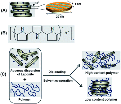 | ||
| Scheme 1 (A) Schematic structure of synthetic laponite clay; (B) oxidized state of polypyrrole; (C) different types of nanocomposites formed by combining polymer and clay particles. | ||
The second component in our nanocomposite is polypyrrole (PPy), a well-known conjugated polymer that is conductive in the doped, oxidized state schematically shown in Scheme 1. This conductive polymer has attracted tremendous interest because of its wide range of applications spanning electrodes for lithium ion batteries to microactuators.13,14 PPy is available in different conducting grades, is dispersible in water and can be processed as a thin film via spin or dip-coating;14 films can also be processed by electro-polymerization but this is beyond the scope of the present paper. The electrochemical behaviour of PPy has been extensively studied in different types of electrolytes, and it has been shown that faradaic processes consisting of a reversible redox reaction dominate the current–voltage (CV) characteristics with a specific capacity of up to 400 F g−1 in aqueous electrolytes.13
Nanocomposites of laponite and polymers have received considerable attention, mostly focusing on mechanical properties. In particular, it has been shown that laponite was effective in improving the stiffness of elastomeric polymers.9
The present paper extends our preliminary note15 that focused on the use of laponite as active electrode material for electrochemical double layer capacitors. The specific capacitance of these laponite film electrodes were even further boosted by intercalating an organo-silane.15 Herein, we propose nanocomposites of laponite–PPy (Lp–PPy), intending to take advantage of the functional properties of both components in order to build robust thin film electrodes for electrochemical energy storage.
Because green energy is due to take a formidable share in the near future, and the issue of energy storage is still not fully solved despite the huge ongoing research activities, devising bottom-up solutions that could yield high energy storage capacities while maintaining low cost and low carbon footprint may contribute to efficiently harnessing and exploiting surplus green energy. We will show in the course of this paper that Lp–PPy nanocomposites can yield highly cost-effective, environmentally friendly and versatile supercapacitor electrodes.
Results and discussion
Structural characterization
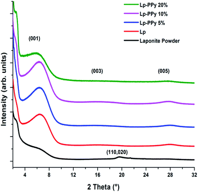
The XRD patterns of Lp powder, Lp and Lp–PPy films are displayed in Fig. 1. The diffraction pattern of the Lp-powder is consistent with a hectorite-type powder pattern showing some disorder in the clay.16 When Lp is dispersed in water and deposited by dip-coating, the clay platelets form a film with the (00L) basal plane oriented parallel to the substrate surface, and the diffraction patterns show a well-defined and intense 001 diffraction peak at 2θ = 6.28°. The full width at half-maximum (FWHM) of the 001 peak is 4.29° for the Lp-powder and decreases to 3.29° for the Lp-film; the calculated interplanar d-spacing is 1.41 nm, and is often referred to as the basal plane spacing.The XRD patterns of the Lp–PPy nanocomposites containing different PPy contents (2 to 20 wt%) show that with increasing PPy content up to 10%, the intensity of the 001 peak slightly increases without noticeable change in FWHM. For the 20% PPy sample, the intensity of this peak decreases and its FWHM increases, suggesting increasing disorder of the Lp-particles. Further, a slight shift in the basal plane diffraction peak to higher d-spacing with increasing PPy concentration is noticed, which indicates an increase of layer spacing, although this shift is difficult to assess due to the large value of FWHM of 001 peak. Using the Bragg's equation, the corresponding d001 increase is from 1.41 nm for the Lp-film to 1.57 nm in the nanocomposite sample, suggesting that the 001 plane of Lp is slightly affected by the presence of PPy (see below for discussion).
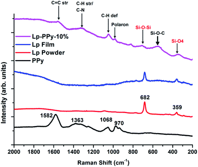
Additional information about the chemical structure of the synthesized Lp–PPy nanocomposites can be obtained using Raman spectroscopy. Fig. 2 shows the Raman spectra of Lp-powder, Lp-film and Lp-10%–PPy nanocomposite as well as pure PPy. In the low energy region, the spectrum shows one band at 682 cm−1 assigned to a Si–O–Si vibration and one band at 359 cm−1 assigned to a Si–O bending vibration.17
Characteristic peaks of PPy (obtained by measuring a drop of pure PPy) appear in the range between 2000 cm−1 and 900 cm−1; they are attributed to C–H stretching and deformation vibrations (1068 cm−1 and 1363 cm−1). A sharp peak at 1582 cm−1 is ascribed to C![[double bond, length as m-dash]](https://www.rsc.org/images/entities/char_e001.gif) C stretching vibrations. The nanocomposite shows in principle the same vibrations of the Lp film in addition to the characteristic vibrations of PPy. But additional peak also observed, the origin of which may be speculated upon as pertaining to Si–O–C vibration. Early work on IR and Raman spectra of some silicon compounds, including substituted disilylacetylene, by Kriegsmann and Beyer18 had shown that the Si–O–C Raman deformation vibration was situated at approximately 507 cm−1, which is close to the somewhat broad peak centred at 540 cm−1. However, it can also be noticed that the valence vibrations attributed to Si–O are somewhat displaced with respect to the values reported by Kriegsmann and Beyer. An explanation may be found in the different materials under investigation. On the basis of these data, we may surmise grafting of PPy on Lp via C–O–Si-bonds.
C stretching vibrations. The nanocomposite shows in principle the same vibrations of the Lp film in addition to the characteristic vibrations of PPy. But additional peak also observed, the origin of which may be speculated upon as pertaining to Si–O–C vibration. Early work on IR and Raman spectra of some silicon compounds, including substituted disilylacetylene, by Kriegsmann and Beyer18 had shown that the Si–O–C Raman deformation vibration was situated at approximately 507 cm−1, which is close to the somewhat broad peak centred at 540 cm−1. However, it can also be noticed that the valence vibrations attributed to Si–O are somewhat displaced with respect to the values reported by Kriegsmann and Beyer. An explanation may be found in the different materials under investigation. On the basis of these data, we may surmise grafting of PPy on Lp via C–O–Si-bonds.
Morphology observations
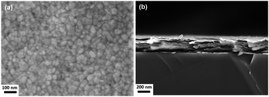
The top-view SEM micrograph (Fig. 3a) shows a homogeneous, nanocrystalline morphology of the Lp film with elongated grains in the size range from 30 to 80 nm. The arrangement of the nanoparticles in the film is probably of the well-known T-type, or edge-to-face bonds19,20 as it arises from the electrostatic interaction between the positively charged particle rim and the negatively charged surface. The scanning transmission electron micrograph (ESI, Fig. S2a†) obtained from thin film areas prepared on a Ni-TEM grid suggests this kind of arrangement.The addition of small amounts of PPy (2 wt%) leads to drastic refinement of the microstructure (Fig. 4a), with no evidence of phase separation, at least to the resolution available for this work. This suggests a different arrangement of the Lp-particles, and indeed close examination of the cross-section micrograph of Fig. 4b reveals that the particles arrange in form of leaflets in which individual elements are glued face-to-face with their edges nearly perpendicular to the substrate surface. This arrangement suggests that PPy grafts on Lp-face (see Raman spectra above) and acts in a similar way to a glue between particles.
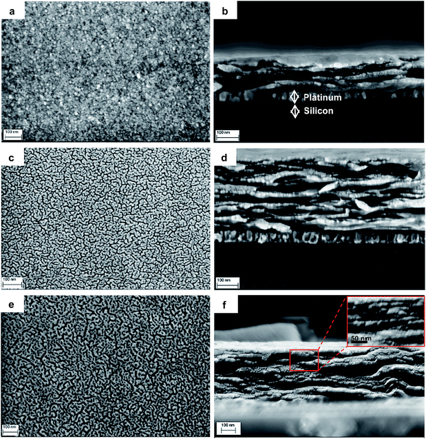 | ||
| Fig. 4 Morphology of Lp–PPy nanocomposites: top views and cross-sections of Lp–PPy-2% (a and b), Lp–PPy-10% (c and d) and Lp–PPy-20% (e and f). Notice the fine structure in (a) that is barely resolved in comparison to Fig. 3a. The arrangement of the Lp nanoparticles (edge nearly perpendicular to substrate surface) is well observed in the cross-section micrographs. In (c and d) the phase separation at the nanoscale is evident: bright nanodomains are LP-rich, the dark, worm-like structure is PPy rich. In (f) one can notice the phase separation in the cross section and the shape of the Lp-platelets in the inset. | ||
With increasing PPy content, the SEM micrographs (Fig. 4c and e) strongly suggest phase separation with the formation of PPy and Lp-rich nanodomains that appear to be interconnected throughout the surface. This phase separation can be observed through film thickness in Fig. 4d and more clearly for Lp–PPy-20% (Fig. 4f). The high-resolution electron backscatter micrograph (ESI, Fig. S2b†) where atomic number contrast depicts PPy (dark) and Lp rich-domains (bright) confirms the nanoscale phase separation. More evidence of this phase separation can also be found in the AFM-micrographs using the force modulation modus of the AFM (ESI, Fig. S3†) that traces differences in the elastic properties of the participating materials.
The results above strongly suggest that the addition of PPy to Lp dispersion leads to a particular arrangement of the Lp-particles in the film with excess PPy being rejected to the interface of the Lp-domains. Due to the specific arrangement of the Lp-domains in the film, excess PPy is thought to meander between the domains throughout film thickness. In general, according to Okamoto et al.,21 a colloidal suspension of Lp and polymer may give rise to three general types of morphology (Scheme 1): (1) intercalated clay composites formed by the insertion of one or more molecular layers of the organic compound into the clay host galleries. (2) Exfoliated clay composites or (3) conventional composites containing clay with the layers non-intercalated in a face-to-face aggregation with segregation between clays and polymer. The results above rather suggest a mechanism of film formation based on grafting of a small fraction of polymer chains on the edges or faces of the Lp particles with excess polymer segregation between the laponite domains thus resulting in phase separation at the nanoscale.
Electrochemical properties
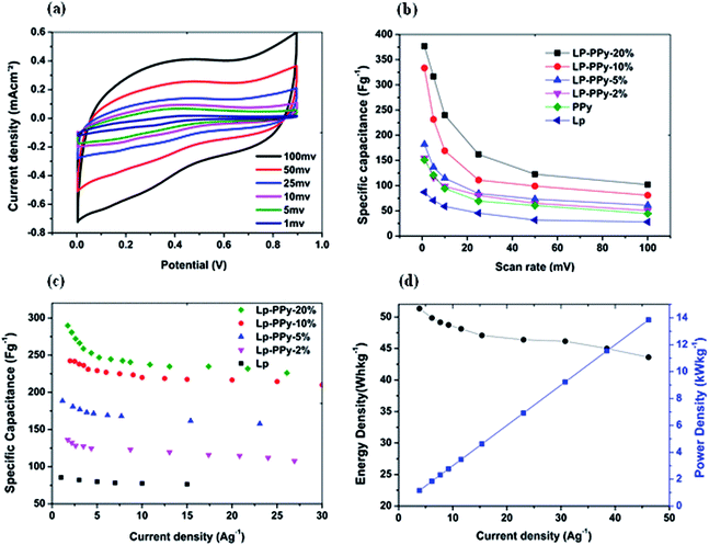
The microstructure depicted above affords a high density of interfaces with a conducting phase (PPy) that meanders between Lp-rich domains throughout film thickness. This structure may therefore be particularly suitable for electrochemical supercapacitors. Because only a small fraction of the film consists of PPy, the cost of such supercapacitor films may be kept low. The capacitive performance of the Lp and Lp–PPy film electrodes was electrochemically tested using cyclic voltammetry (CV) measurements in the potential window from 0 to 0.9 V at various scan rates. It is well-known that PPy behaves as pseudocapacitor following a well-known redox reaction22 in the negative voltage range, using non-aqueous electrolytes. Because the electrolyte used in this work is an aqueous solution of KCl, we have deliberately opted for the voltage range above and avoided negative voltages where hydrogen evolution is set to take place which would interfere with our results, e.g., through redox-reactions of the Pt-layer of the substrate. Bearing the latter in mind, the CV behaviour of the nanocomposite is exemplary for Lp–PPy-20% electrode in Fig. 5a where only the last curve of 50 cycles that are necessary for stabilization is depicted. The curves have nearly rectangular shape that indicates a good double-layer capacitive behaviour under the measured scan rates, and quick dynamics of charge propagation (for the plain film, see ESI, Fig. S4a†). With increasing scan rate, the CV curves gradually deviate from rectangular shape. This behaviour may be explained with the charge–discharge process of composites in the KCl aqueous electrolyte, which is associated with the insertion of K+ into the hybrid material and release of Na+ to the electrolyte as reported by He et al.23 At a low scan rate (e.g. 1 mV s−1), the ions have enough time (the mean ionic penetration depth is generally proportional to the square root of time) to diffuse into most of the accessible spaces of the hybrid composite, but at higher scan rates, e.g., of 100 mV s−1, the K+ ions can only reach the outer surface of the nanocomposite material and the internal part has little contribution to the electrochemical capacitive behaviour.The specific capacitance of Lp, PPy and Lp–PPy electrodes is calculated from the CVs (ESI, Fig. S4†) following the procedure outlined in the Experimental section, and the dependence of the specific capacitance on the scan rate is depicted in Fig. 5b that shows the well-known downward trend with increasing scan rate. At 1 mV s−1, the specific capacitance obtained for the nanocomposite increased with increasing Lp–PPy ratio from 87 F g−1 for the Lp film to 350 F g−1 for Lp–PPy-20% (Table 1). These values are higher than the range of values reported for carbon-based materials, including carbon nanotubes, and are very similar to those reported for plain PPy electrodes.13,24,25
| Sample | Lp powder | Lp | Lp–polyp 2 | Lp–PPy 5 | Lp–PPy 10 | Lp–PPy 20 |
|---|---|---|---|---|---|---|
| a Estimated from SEM micrographs. b Specific capacitance at 1 mV s−1. | ||||||
| Composition | ||||||
PP–Lp (wt![[thin space (1/6-em)]](https://www.rsc.org/images/entities/char_2009.gif) : :![[thin space (1/6-em)]](https://www.rsc.org/images/entities/char_2009.gif) wt)% wt)% |
— | 0 | 2 | 5 | 10 | 20 |
| Thickness (nm)a | — | 370 | 350 | 320 | 320 | 400 |
![[thin space (1/6-em)]](https://www.rsc.org/images/entities/char_2009.gif) |
||||||
| XRD/001 peak | ||||||
| 2θ (°) | 6.33 | 6.31 | 6.25 | 6.18 | 5.9 | 5.65 |
| d 001 (nm) | 1.41 | 1.39 | 1.42 | 1.44 | 1.49 | 1.57 |
| FWHM (°) | 5.5 | 3.43 | 3.4 | 3.46 | 4.15 | 4.9 |
![[thin space (1/6-em)]](https://www.rsc.org/images/entities/char_2009.gif) |
||||||
| Electrochemical | ||||||
| Capacitance (F g−1)b | — | 87 | 154 | 181 | 320 | 350 |
The cause for this higher capacitance could be attributed to the higher conductivity pertaining to the PPy phase and the larger surface that arises from the nanoscale phase separation. The electronic charge path is thought to follow the meandering PPy phase throughout film thickness to the collector electrode.
In this respect, the higher value of specific capacitance obtained for Lp–PPy-20% may be attributed to a combination of higher conductivity and large surface area accessible to ionic species, because it is well know that double layer capacitance per unit of external surface area is strongly dependent on surface morphology and porosity.26,27 For practical applications, the galvanostatic charging–discharging behaviour is more appropriate to describe the performance of the electrode. Fig. 5c shows the charging–discharging curves at 3 A g−1 for the different electrodes investigated in the potential range from 0 to 0.6 V. The charging–discharging curves are triangular in shape with linear charging–discharging behaviour that is characteristic for double layer capacitors, and denotes good charge–discharge reversibility and an ideal capacitive behaviour (ESI, Fig. S4b†). The specific capacitance can then be obtained from the slope of the charge–discharge curve according to the procedure described in the Experimental section. Fig. 5c shows that the specific capacitance is nearly constant for all current densities investigated, with values ranging from 80 F g−1 for the plain Lp film and from 136 to 290 F g−1 for increasing PPy content from 2 to 20%. The long term behaviour was investigated at 3 A g−1 for 500 cycles without noticeable change in the specific capacitance (ESI, Fig. S5†). Energy density and power density are additional important factors that characterize the performance of the capacitor electrode. Using the galvanostatic charge–discharge curves, the energy and power densities can be calculated using eqn (1) and (2) as follows:
| De = 1/2CV2 | (1) |
| Dp = De/Δt, | (2) |
In addition to cyclic voltammetry, the capacitive behaviour of the Lp and Lp–PPy nanocomposite films is further investigated using electrochemical impedance spectroscopy (EIS) in three-electrode cell measurements in KCl electrolyte.
Fig. 6 presents the Nyquist plots of the Lp and Lp–PPy-10% samples tested in 1 M KCl. The Nyquist plot represents the behaviour of an electrical double layer capacitor, which can be easily described by a series resistance (Rs) related to the bulk electrolyte and to the involved faradic process29,30 and a double layer capacitance (Cdl) related to the charge accumulation at the electrode/electrolyte interface.
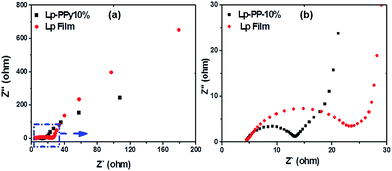 | ||
| Fig. 6 (a) Nyquist plots of the EIS for Lp and Lp–PPy-10% sample (b) the magnified part of the semicircles. | ||
From the Nyquist plot, a charge transfer resistance can be obtained from the diameter of the semicircle. At high frequency (i.e., at low resistance Z′ values), the impedance implies the conductivity of both active materials and electrolyte. The high-to-medium frequency region shows pseudocharge transfer resistance, which is associated with the porous structure of the nanocomposite. The low frequency range (i.e., at high resistance Z′ values) of the impedance characterizes pure capacitive behaviour. Theoretically, an ideal double layer capacitor should display a parallel line to the imaginary axis of the Nyquist plot. However, in our case, the plot shows a line with an inclined angle between 45° and 90° against the real axis, denoting the existence of pseudocapacitive processes31 that are probably related to the redox reactions of PPy.32
From the diameters of the semicircle, the charge-transfer resistance of Lp and Lp–PPy-10% was calculated to be 15 and 7 Ω, respectively. The high resistance of the pristine Lp sample indicates its poor conductive properties. The relatively low resistance obtained for Lp–PPy-10% may be explained by the particular nanoscale structure discussed above that affords efficient pathways for charge transport.
Experimental section
Materials
Laponite RD, synthetic smectic clay with a density of 2.65 g cm−3, was obtained from Southern Clay Products and used as received without any further purification. Doped polypyrrole, high-conductivity grade, dispersed in water was purchased from Aldrich (Germany). Deionized water was used to prepare aqueous solutions.Preparation of laponite–polypyrrole solutions
Lp–PPy mixture was prepared as follows. First a 1% of well-dispersed clay suspension was prepared by adding 0.5 g of Lp nanoparticles into 50 mL of water (at a pH of 9.6). The dispersion was stirred at room temperature overnight. A dispersion of PPy (5% in water), was then added to Lp sol in various weight ratios to obtain the clay–polymer mixture in its final aqueous form. The mixture was stirred for 24 hours at room temperature and ultrasonicated for around 15 minutes before use.Lp–PPy films elaboration
Large particles were removed from the solution by filtration (1.2 μm filter) before coating. The films were deposited by dip-coating in a glove box onto cleaned substrates with a withdrawal speed of 100 mm min−1. Platinized silicon wafers were used as substrates. The coating layer was dried at 80 °C for 15 hours. High quality transparent films are obtained and studied at room temperature. The film thickness was in the range from 320 to 400 nm, determined from SEM cross sections.Sample series were fabricated via dip coating for electrochemical tests and structural characterization. The first consisted of pure Lp films, the second of Lp–PPy of various percentages of PPy. Samples were designated Lp–xPPy where x is the PPy–Lp ratio (wt![[thin space (1/6-em)]](https://www.rsc.org/images/entities/char_2009.gif) :
:![[thin space (1/6-em)]](https://www.rsc.org/images/entities/char_2009.gif) wt).
wt).
Materials characterization
Atomic force microscopy (AFM, Nano wizard, JPK Instruments, Berlin) images were obtained in tapping mode using super-sharp silicon tips (Nanosensors, Neuchatel, Switzerland).
A Bruker Raman microscope (SINTERRA, Bruker, Germany) was used to acquire Raman scattering spectra over a range of 70−3600 cm−1, with a spectral resolution of 3–5 cm−1, using a backscattering configuration with a 20× objective excited with a 532 nm laser diode. Data were collected on numerous spots on the sample and recorded with a fully focused laser power of 20 mW. Each spectrum was accumulated four times with an integration time of 10 s. The Raman signal was recorded using a CCD camera. Silicon substrate Raman peak position (520 cm−1) was used to calibrate spectral frequency.
To measure the capacitance of the electrodes, CVs were recorded in an aqueous electrolyte containing 1 M KCl between 0 V and 0.9 V at different scan rates. The charge–discharge behaviour at different current densities and long-term cycling stability were tested in 1 M KCl. Before each electrochemical experiment, N2 was bubbled in the electrolyte for 30 min. The electrochemical experiments were conducted on a minimum of three to five samples each. The specific capacitances were calculated from the CVs using the equation given below:33
| C = I/(2VSm), | (3) |
From the slope of the charge–discharge curve, the specific capacitance can then be deduced according to the following:
| C = It/(Vm), | (4) |
Conclusions
In the present work Lp–PPy nanocomposites containing 2–20% of PPy were investigated. With increasing PPy content, evidence of a phase separation at the nanoscale is obtained with the formation of Lp and PPy rich nanodomains. The PPy phase appears to meander through film thickness down to substrate surface. The high surface area obtained through the nanoscale phase separation together with the well-known conductivity of the polypyrrole phase affords promising nanocomposite electrodes for supercapacitor applications. The electrodes combine high specific capacitance with promising retention rates and long term stability. More important advantages may be seen in the robustness of the nanocomposite and its cost-effectiveness because: (i) the Lp-nanomaterial acts as reinforcing component for the polymer; (ii) the amount of the expensive PPy phase is reduced to few tens of a percent. Moreover, because processing is from aqueous suspensions at ambient atmosphere and curing temperatures are below 90 °C, the films are environmentally friendly. Further, they can be deposited on electroded polymer sheets in a continuous process, thus allowing electrode coils to be fabricated, and therefore making industrial scale-up an easy issue.Acknowledgements
Financial support of this work is provided by the EU-program INTERREG IVA-Southern Denmark-Schleswig-K.E.R.N.-Project# 111-1.2-12 “SuperCap”.Notes and references
- (a) C. Sanchez, P. Belleville, P. M. Popall and L. Nicole, Chem. Soc. Rev., 2011, 40, 696 RSC; (b) G. M. Nascimento, V. R. L. Constantino, R. Landers and M. L. A. Temperini, Macromolecules, 2004, 37, 9373 CrossRef.
- M. I. Carretero and M. Pozo, Appl. Clay Sci., 2010, 47, 171 CrossRef CAS PubMed.
- V. Rives, M. del Arco and C. Martín, Appl. Clay Sci., 2014, 88–89, 239 CrossRef CAS PubMed.
- J. I. Dawson and R. O. C. Oreffo, Adv. Mater., 2013, 25, 4069 CrossRef CAS PubMed.
- Z. P. Xu, J. Zhang, M. O. Adebajo, H. Zhang and C. Zhou, Appl. Clay Sci., 2011, 53, 139 CrossRef CAS PubMed.
- S. Navalon, M. Alvaro and H. Garcia, Appl. Catal., B, 2010, 99, 1 CrossRef CAS PubMed.
- C. Belver, P. Aranda and E. Ruiz-Hitzky, J. Mater. Chem. A, 2013, 1, 7477 CAS.
- S. M. Lee and D. Tiwari, Appl. Clay Sci., 2012, 59, 84 CrossRef PubMed.
- S. M. Liff, N. Kumar and G. H. McKinley, Nat. Mater., 2007, 6, 76 CrossRef CAS PubMed.
- V. L. Reena, C. Pavithran, V. Verma and J. D. Sudha, J. Phys. Chem. B, 2010, 114, 2578 CrossRef CAS PubMed.
- S. Letaïef, A. Martín-Luengo, P. Aranda and E. Ruiz-Hitzky, Adv. Funct. Mater., 2006, 16, 401 CrossRef.
- H. He, Q. Tao, J. Zhu, P. Yuan, W. Shen and S. Yang, Appl. Clay Sci., 2013, 71, 15 CrossRef CAS PubMed.
- T. V. Vernitskaya and O. N. Efimov, Russ. Chem. Rev., 1997, 66, 443 CrossRef PubMed.
- E. Smela, J. Micromech. Microeng., 1999, 9, 1 CrossRef CAS.
- M. Fatnassi, C. H. Solterbeck and M. Es-Souni, RSC Adv., 2014, 87, 46976 RSC.
- H. van Olphen and J. J. Fripiat, Data handbook of clay materials and other non-metallic minerals, OECD and Clay Minerals Society, Pergamon Press, New York, 1979 Search PubMed.
- Y. Sekine and T. Ikeda-Fukazawa, J. Chem. Phys., 2009, 130, 034501 CrossRef PubMed.
- H. Kriegsmann and H. Beyer, Z. Anorg. Allg. Chem., 1961, 311, 180 CrossRef CAS.
- H. van Olphen, An Introduction to Clay Colloid Chemistry, Wiley, New York, 1977 Search PubMed.
- M. Dijkstra, J.-P. Hansen and P. A. Madden, Phys. Rev. E: Stat. Phys., Plasmas, Fluids, Relat. Interdiscip. Top., 1997, 55, 3044 CrossRef CAS.
- S. Ray and M. Okamoto, Prog. Polym. Sci., 2003, 28, 1539 CrossRef CAS PubMed.
- A. F. Diaz, J. I. Castillo, J. A. Logan and W.-Y. Lee, J. Electroanal. Chem., 1981, 129, 115 CrossRef CAS.
- J. Zhu and J. He, ACS Appl. Mater. Interfaces, 2012, 4, 1770 CAS.
- T. Chen and L. Dai, Mater. Today, 2013, 16, 272 CrossRef CAS PubMed.
- D. N. Futaba, K. Hata, T. Yamada, T. Hiraoka, Y. Hayamizu, Y. Kakudate, O. Tanaike, H. Hatori, M. Yumura and S. Iijima, Nat. Mater., 2006, 5, 987 CrossRef CAS PubMed.
- H. Shi, Electrochim. Acta, 1996, 41, 1633 CrossRef CAS.
- N. Brun, S. R. S. Prabaharan, C. Surcin, M. Morcrette, H. Deleuze, M. Birot, O. Babot, M.-F. Achard and R. Backov, J. Phys. Chem. C, 2012, 116, 1408 CAS.
- D. W. Wang, F. Li, M. Liu, G. Q. Lu and H. M. Cheng, Angew. Chem., Int. Ed., 2008, 47, 373 CrossRef CAS PubMed.
- K. Liang, X. Tang and W. Hu, J. Mater. Chem., 2012, 22, 11062 RSC.
- G. Han, Y. Liu, E. Kan, J. Tang, L. Zhang, H. Wang and W. Tang, RSC Adv., 2014, 4, 9898 RSC.
- L. Cui, J. Li and X. G. Zhang, J. Appl. Electrochem., 2009, 39, 1871 CrossRef CAS.
- H. Liu, P. He, Z. Li, Y. Liu and J. Li, Electrochim. Acta, 2006, 51, 1925 CrossRef CAS PubMed.
- K. W. Nam and K. B. Kim, J. Electrochem. Soc., 2002, 149, 346 CrossRef PubMed.
Footnotes |
| † Electronic supplementary information (ESI) available. See DOI: 10.1039/c4ra16540c |
| ‡ M. Fatnassi and M. Es-Souni contributed equally to this work. |
| This journal is © The Royal Society of Chemistry 2015 |

