
 Open Access Article
 This Open Access Article is licensed under a
 Creative Commons Attribution 3.0 Unported Licence
The Zn-vacancy related green luminescence and donor–acceptor pair emission in ZnO grown by pulsed laser deposition
Zilan
Wang
a,
S. C.
Su
a,
M.
Younas
a,
F. C. C.
Ling
*a,
W.
Anwand
b and
A.
Wagner
b
aDepartment of Physics, The University of Hong Kong, Pokfulam Road, Hong Kong, P. R. China. E-mail: ccling@hku.hk
bInstitute of Radiation Physics, Helmholtz-Zentrum Dresden-Rossendorf, Bautzner Landstr. 400, 01328 Dresden, Germany
First published on 14th January 2015
Abstract
A low temperature (10 K) photoluminescence study shows that green luminescence (GL) peaking at 2.47 eV and near band edge (NBE) emission at 3.23 eV are introduced in undoped ZnO grown by pulsed laser deposition (PLD) after 900 °C annealing. The NBE emission exhibiting blue shift with increasing temperature is assigned to the transitions of the donor–acceptor-pair (DAP)/free-electron-to-acceptor (FA). Positron annihilation spectroscopy (PAS) study shows that the introduction of the GL is correlated with the formation of the Zn vacancy-related defect (VZn). Comparing the transition energies of VZn obtained by the previous first principles calculation [Janotti and Van de Walle, Phys. Rev. B: Condens. Matter Mater. Phys., 2007, 76, 165202], the GL is associated with the transition from the conduction band to the ε(−/2−) state of VZn and the DAP/FA emission involves the acceptor level ε(0/−) of VZn.
Introduction
ZnO has attracted extensive attention as a potential material for a variety of device applications, including optoelectronics operating in the wavelength range of ultra-violet (UV), solid-state white lighting, and sensors.1,2 Based on the ZnO-related structures, UV light emitting diode (LED) fabrication and low threshold UV lasing have been achieved.3–8 However, the realization of practical ZnO-based optoelectronic devices is still hindered by the asymmetric p-type doping difficulty.1,2 Results of recent p-type doping studies suggest that more exact and detailed knowledge concerning the physics of the defects and the corresponding control is needed to achieve reliable p-type doping in ZnO. However, the understanding of defects in ZnO is far from complete and controversial.One of the controversial assignments of defect spectroscopic signal in ZnO is the green luminescence (GL). GL is a broad defect emission peaking at 2.3–2.5 eV, which has been associated with Cu-impurity,9 Zn-vacancy,10–13 O-vacancies,14–16 Zni-related complexes,17 and oxide antisite defects.18 It is generally accepted that the GL with the fine structure is originated from the Cu impurity and the structureless GL is associated to the intrinsic defects. Ton-That et al.19 identified two kinds of GL's having peak positions at 2.30 eV and 2.53 eV respectively in the O-rich and Zn-rich ZnO samples, and they are respectively assigned to VZn and VO. Lv and Li20 show that the peak positions and shapes of the GL's observed in their ZnO powder samples depend on the abundance of the VO, VZn and Oi defects. These recent results show that there are more than one origins of GL's associated with the different intrinsic defects in ZnO. Donor–acceptor pair (DAP) emission at 3.220 eV has been observed in undoped ZnO at the temperature of 5 K.21 As temperature increases, the 3.220 eV emission quenches and the 3.236 eV free electron to acceptor (FA) emission emerges because of the thermal ionization of the shallow donors. The acceptor level was found to be 195 ± 10 meV and the acceptor was attributed to NO.
In the present study, undoped ZnO films are grown on sapphire by pulsed laser deposition (PLD) with different substrate temperatures and oxygen pressures. Low temperature PL study shows that after annealing at 900 °C, the GL (peaking at 2.47 eV) originated from a single type of defect and the near band emission (3.23 eV) are created. Positron annihilation spectroscopy (PAS) is employed to reveal the origin of the emissions. The origins of the emissions will also be discussed by making comparison to the previous results of first principle calculations.
Experimental
Undoped ZnO films with thickness of 300 nm were grown on the c-plane sapphire using the method of PLD. To carry out a systematic study and to obtain a conclusive result, films are grown with different substrate temperatures (Tsub = 300 °C and 600 °C) and oxygen pressures (P(O2) = 0 Pa, 1.3 Pa and 5 Pa). The ZnO target (99.999% impurity) is obtained from Kurt J. Lesker Co. The background pressure for the growth is 10−4 Pa. The 248 nm laser pulse having the pulse energy of 300 mJ and repetition rate of 2 Hz from the Coherent COMPexPro 102 excimer laser is used for the PLD growth. Isochronal post-growth annealing was carried out at different temperatures with the period of 40 minutes in Ar atmosphere. Another piece of ZnO sample was placed on top of the sample being studied during the annealing in order to prevent the surface damage during the annealing process. The samples thus fabricated have been systematically and comprehensively characterized by a variety of spectroscopies including Atomic force microscopy (AFM), X-ray diffraction (XRD), secondary ion mass spectroscopy (SIMS), Hall measurement, Raman spectroscopy, and PAS. The details of the results can be found in ref. 22.For the PL measurement, the 325 nm line from the Kimmon 30 mW He–Cd laser is used as the excitation source. The 500 mm focal length monochrometer, the photomultiplier (PMT), and the lock-in amplifier are used for the spectrum acquisition. The samples are loaded in the Oxford Instrument 10 K closed cycle He refrigerator for controlling the sample temperature.
The PAS measurement is carried out with a mono-energetic positron beam having the maximum positron incident energy of 25 keV. The annihilation gamma ray energy spectra are detected by a high purity Ge detector system having the energy resolution of 1.3 keV at the 514 keV gamma line. The energy window for the S-parameter is 511 ± 0.76 eV, and those for the W parameter are 511 ± 3.4 eV and 511 ± 6.8 eV.
Results and discussion
The XRD spectra of all the samples exhibit only the (002) and (004) peaks. The full width at the half maximum (FWHM) of the (002) peak is 0.21–0.25° for the as-grown samples grown at 300 °C, and improve to ∼0.12° after the 900 °C annealing.Fig. 1(a) shows the 10 K PL spectra of the samples grown at Tsub = 300 °C without oxygen annealed at different temperatures. The defect emission of the sample annealed at 600 °C has the peak at ∼2.2 eV. As the annealing temperature increases, the peak position, intensity, and width of the GL band would be blue-shifted, increased, and narrowed respectively. After annealing at 900 °C, the peak position is blue-shifted to 2.47 eV. For the other samples grown with the different initial conditions, similar thermal evolution in the spectral features is observed, although the exact shape of the GL band depends on the initial growth conditions. The 10 K PL spectra of the samples grown at different initial growth conditions and annealed at 900 °C are shown in Fig. 1(b). The corresponding normalized spectra are shown in the insert of Fig. 1(b). It clearly demonstrates that the same GL band peaking at 2.47 eV is yielded after the 900 °C annealing regardless of the initial growth parameters.
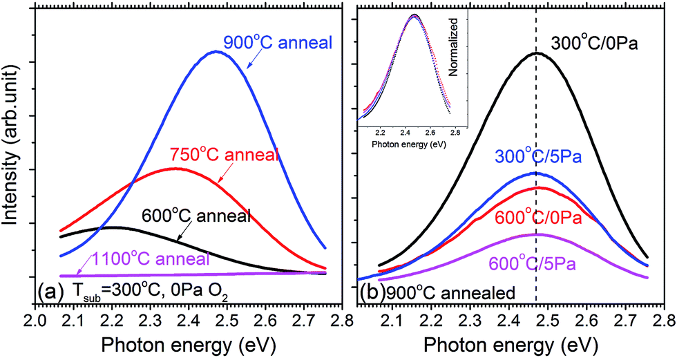 | ||
| Fig. 1 The low temperature (10 K) PL spectra of (a) the undoped ZnO samples grown at the substrate temperature of 300 °C without oxygen subjected to post-growth annealing at different temperatures; and (b) the undoped ZnO samples grown with the different substrate temperatures Tsub and oxygen pressures P(O2) (Tsub/P(O2)) subjected to the post-growth annealing of 900 °C. The insert of (b) shows the normalized spectra in (b). | ||
The thermal evolution of the GL in the undoped samples can be understood as follows. The GL's of the samples annealed at temperatures lower than 900 °C are the superposition of the defect emissions contributed from more than one defect origins. As the samples grown at different conditions and annealed at different temperatures would have different compositions of the involved defects, the shape and the peak position of the resultant GL (which is governed by the relative composition of the different defects20) is thus dependent on the annealing temperature and the initial growth parameters. However as the annealing temperature increases to 900 °C, all the samples irrespective of the initial growth condition exhibit the GL with the same peak position and shape. The GL bands of all the samples annealed at 900 °C (peaked at 2.47 eV as seen in Fig. 1(b)) are originated from a single type of defect. The other defects contributed for the GL bands as found in the samples annealed at temperatures lower than 900 °C are thermally removed. It is also noticed that the 2.47 eV defect emission disappears after the temperature of 1100 °C (see Fig. 1(a)).
Fig. 2(a) and (b) show the temperature dependent PL spectra of the samples grown at Tsub = 600 °C and P(O2) = 1.3 Pa annealed at 750 °C and 900 °C respectively. For the sample annealed at 750 °C, the peak position of the PL spectra is at 2.31 eV at 10 K. The peak position shifts to higher energy and the intensity decreases with increasing temperature. This could be understood as that the emissions from the different defects have different quenching dependence on the measuring temperature. For the PL spectrum of the sample annealed at 900 °C which is originated from the single type of defect, the peak position does not have significant change and the intensity reduces while the measuring temperature increases as expected. This result is typical for all the sample sets grown with the different initial growth conditions.
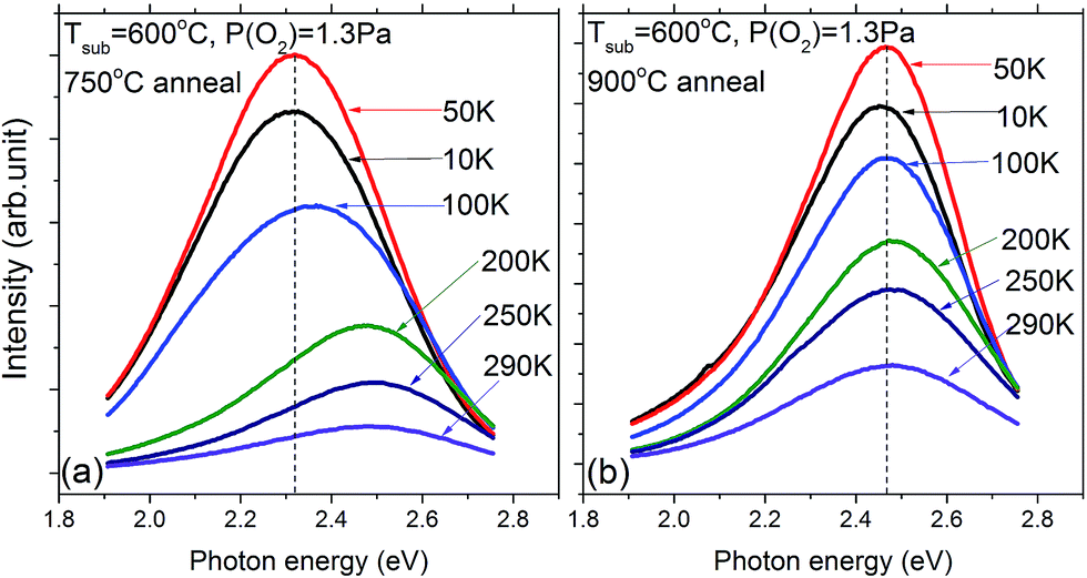 | ||
| Fig. 2 The temperature dependent PL spectra of the undoped ZnO samples grown at Tsub = 600 °C and P(O2) = 1.3 Pa after the post-growth annealings of (a) 750 °C; and (b) 900 °C. | ||
Room temperature PAS study is carried out to investigate the origin of the 2.47 eV GL. Zn-vacancy has low formation energy in n-type ZnO23 and is the important acceptor in ZnO single crystal.24 At room temperature, PAS is selectively sensitive to the Zn-vacancy related defects in ZnO. The S and W parameters are used to monitor the Doppler broadening of the line shape of the 511 keV positron-electron annihilation peak. For all the samples, the plots of the S-parameter (and also the W-parameter) against the positron incident energy (E) show plateaus at E ∼ 5 keV, which correspond to the mean positron implantation depth of ![[x with combining macron]](https://www.rsc.org/images/entities/i_char_0078_0304.gif) ≈ 100 nm. While the film thickness is 300 nm, the S-parameter (and also the W-parameter) of each of the films is taken at E = 5 keV.
≈ 100 nm. While the film thickness is 300 nm, the S-parameter (and also the W-parameter) of each of the films is taken at E = 5 keV.
It is well known that the same single type of Zn-vacancy related defect would present as a straight line in the S–W plot. The S–W parameter plot of the samples grown at the Tsub/P(O2) of 300 °C/0 Pa, 600 °C/0 Pa, and 600 °C/1.3 Pa are shown in Fig. 3. The insert shows the zoom-in of the marked region in Fig. 3. The samples that exhibit the GL peaked at 2.47 eV are marked by the green rectangles.
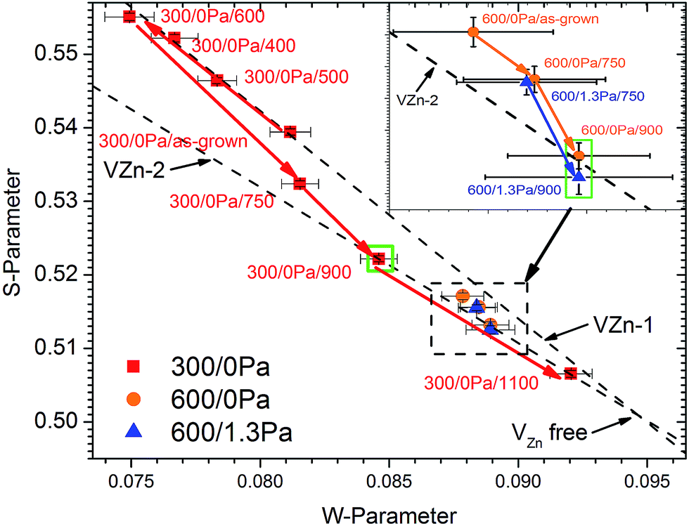 | ||
| Fig. 3 The S–W plots of the three sets of undoped ZnO samples fabricated at different Tsub/P(O2) of 300 °C/0 Pa, 600 °C/0 Pa, and 300 °C/1.3 Pa subjected to post-growth annealing at different temperatures. The zoom-in of the dash-lined enclosed region is shown in the insert. The arrows indicate the thermal induced conversions to the VZn-2 defect. The samples exhibiting the GL with the peak at 2.47 eV are marked by the green rectangles. | ||
In the previous study on the ZnO samples grown by the same method,22 two kinds VZn-related defects (namely VZn-1 and VZn-2) having different microstructures are identified, and their corresponding characteristic straight lines are reproduced in Fig. 3. The intersection of the two straight lines is the S–W value of the ZnO bulk state.22 For the present 300 °C/0 Pa sample, the S–W data of the as-grown and the samples annealed at Tanneal < 750 °C lie on the straight line of VZn-1, indicating that single type of VZn-1 defect exists in these samples. At Tanneal = 900 °C, the VZn structure transits to the VZn-2 structure. Similar transition to the VZn-2 structure is also observed in the 600 °C/0 Pa, and 600 °C/1.3 Pa samples after the 900 °C annealing (insert of Fig. 3). To conclude the PAS story, the transition to the Zn-vacancy microstructure of VZn-2 occurs at 900 °C in all the samples, which exactly coincides with the introduction of the 2.47 eV GL. The GL peaked at 2.47 eV observed after the annealing of 900 °C is thus associated to the Zn-vacancy related defect VZn-2. From Fig. 3, the S-parameter of the sample grown at 300 °C/0 Pa decreases (and thus so does the concentration of VZn-2) after the annealing of 1100 °C. This is consistent with the observation that the GL having the 2.47 eV peak anneals out after the annealing of 1100 °C is performed (as shown in Fig. 1(a)).
The low temperature (10 K) near band edge PL spectra of the 600 °C/1.3 Pa samples annealed at different temperatures are shown in the insert of Fig. 4. The 3.356 eV line observed in the as-grown sample is assigned to the neutral donor bound exciton (D0X) emission.25 Its first and second LO-phonon replicas are also observed. The peak positions of the D0X, 1LO (D0X) and 2LO (D0X) are shown in Fig. 5, showing that their peak positions are red-shifted with the increasing temperature.
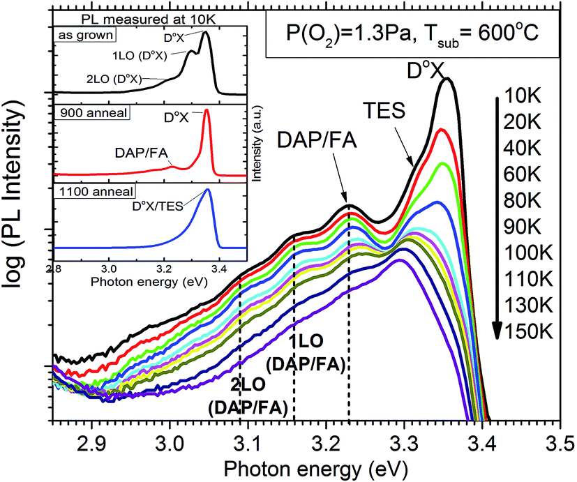 | ||
| Fig. 4 The temperature dependent NBE PL spectra of the undoped ZnO sample grown at Tsub = 600 °C and P(O2) = 1.3 Pa after the 900 °C post-growth annealing. The PL intensity is plotted with the log scale. The insert shows the low temperature (10 K) near band edge PL spectra of the as-grown sample, the samples annealed at 900 °C and 1100 °C with the PL intensity in normal scale. | ||
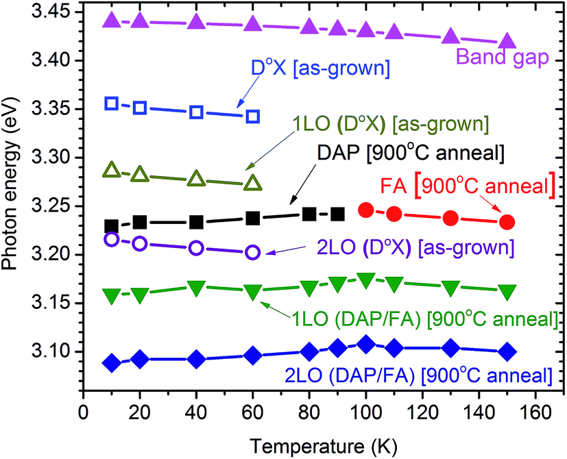 | ||
| Fig. 5 The peak positions of some NBE emissions versus the measuring temperature. The samples are grown at Tsub = 600 °C and P(O2) = 1.3 Pa. These peaks include the D0X and its first two LO replicas identified in the as-grown sample, as well as the DAP/FA emissions and its two LO replicas identified in the sample annealed at 900 °C. The band gap calculated by the Varshni equation is also included for reference. | ||
The low temperature (10 K) near band edge PL spectrum of the 600 °C/1.3 Pa sample annealed at 900 °C is shown in the insert of Fig. 4, and the corresponding temperature dependent PL spectra with the PL intensity plotted in log scale are shown in Fig. 4. The D0X (and its two-electron satellite (TES)26) emissions persist after the sample is annealed at 900 °C. As the measuring temperature increases, the D0X and TES peaks red-shift with their intensity decreased, and they merge at 80 K (Fig. 4). A peak of 3.229 eV is found in the low temperature PL spectrum of this sample (Fig. 4). This peak cannot be the first and second phonon replicas of the D0X observed in the as-grown sample as it exhibits blue-shift with increasing temperature (Fig. 4 and 5). One of the possible origins of this 3.229 eV peak is associated with the free exciton (FX) emission of ∼3.37 eV, which has been observed in the low temperature PL spectra of ZnO.27,28 Its second LO-phonon replica (2LO (FX)) would overlap with this 3.229 eV peak, and the observed blue-shift could be due to the transition from the D0X emission to the FX emission as the temperature increases. Another possible origin of the 3.229 eV emission is the donor–acceptor-pair (DAP) transition. The blue shift is due to the enhancement of the free-electron-to-acceptor (FA) emission because of the shallow donor ionization as the measuring temperature increases.
Teke et al.28 have studied the excitonic fine structure of high quality wurtzite structure ZnO single crystal produced by Cermet Inc. The intrinsic excitonic features are significantly strengthened with the forming gas annealing due to the improvement of the crystal quality of the surface. Phonon replicas 1LO (FX), 2LO (FX), and 3LO (FX) are observed in the post-growth forming gas annealed sample. The 3LO (FX) are very weak and barely detectable. In the present study, higher order LO-phonon replicas of the 3.229 eV are also observed at 3.163 eV and 3.093 eV in the low temperature (10 K) PL of Fig. 4. If the 3.229 eV peak is associated with the 2LO of the FX emission, then the 3.163 eV and 3.093 eV would be the 3LO (FX) and 4LO (FX) respectively. The peak positions of these two phonon replicas are also observed to be blue-shifted by the increasing temperature (see Fig. 5). Though not specified in Teke et al.,28 the high crystalline quality ZnO single crystal produced by Cermet has typical electron mobility of larger than 200 cm2 V−1 s−1. For the present PLD grown samples annealed at 900 °C, the electron mobility is 50–95 cm2 V−1 s−1 depending on the initial growth oxygen pressure.22 The observation of the 4LO (FX) in the PLD grown film (expected to have inferior crystalline quality than the single crystal in Teke et al.28) is thus less likely tenable. Moreover if the 3.229 eV in the 10 K PL spectrum is the 2LO (FX), the corresponding stronger 1LO (FX) is expected to be presence at ∼3.299 eV in the same spectrum. However such peak cannot be found. The 3.229 eV in the low temperature PL spectrum is thus plausibly assigned to the DAP/FA emission, while the 3.163 eV and 3.093 eV are the corresponding 1LO (DAP/FA) and 2LO (DAP/FA).
The peak position of the DAP/FA as a function of the measuring temperature is shown in Fig. 5. The band gap calculated by the Varshni equation is also included. As the temperature increases, the DAP/FA peak increases from 3.229 eV at 10 K to the maximum of 3.246 eV at 100 K and then decreases. The increase of the photon energy with increasing temperature at temperature below 100 K is associated with the enhancement of the FA emission induced by the shallow donor ionization. At temperatures higher than 100 K, the red-shift of the peak is related to the increase of the band gap and thus the decrease of the photon energy. The relations between the donor level ED, acceptor level EA, the photons energies of the FA (EFA) and DAP (EDAP) emissions are given by:21
| ED = [EFA(T) − kBT/2] − [EDAP(T) − αND1/3] | (1) |
| EA = [Eg(T) − ED] − [EDAP(T) − αND1/3] | (2) |
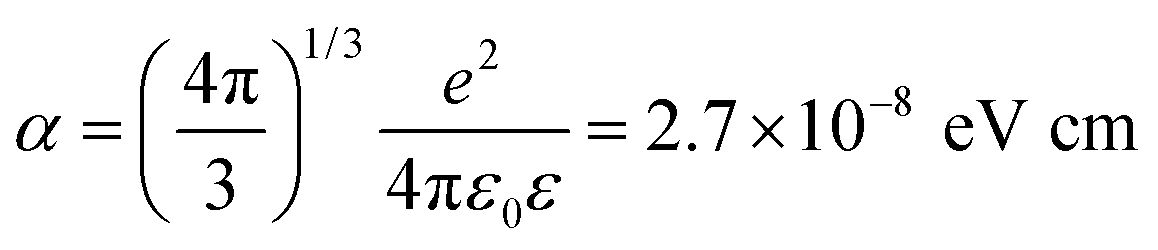
To calculate the acceptor level EA, ED in eqn (1) is substituted into eqn (2) and the term EDAP(T) − αND1/3 is found to be cancelled, which yields:
| EA = Eg(T) − EFA(T) + kBT/2 | (3) |
Taking the approximation that the transition is pure FA at the high temperature (say 100 K, i.e. EFA(100 K) = 3.246 eV), EA can be calculated to be 188 ± 9 meV from eqn (3) with the Eg(100 K) obtained through the Varshni equation.
At the temperature of 1100 °C annealing, the D0X/TES merged peak becomes broadened (insert of Fig. 4) and it is difficult to determine unambiguously whether the DAP/FA peak exists. However by monitoring the first and the second phonon replicas of the DAP/FA in the log scaled PL spectra, they do not exist in the PL spectrum of the samples annealed at 1100 °C.
Thonke et al.21 observed the DAP emission (3.220 eV) in the PL spectrum of ZnO measured at 5 K, and the FA emission (3.236 eV) emerged at the temperature of 40 K. The corresponding acceptor was found to have EA = 195 ± 10 meV, which is similar to the EA found in the present study. While considering the possible candidate for the acceptor, the EA value was compared with the theoretical values available at that time. Thonke et al.21 ruled out the possibility of assigning the acceptor to Zn-vacancy as Zn-vacancy was taken as the singly ionized acceptor with EA ∼ 0.8 eV.21 The acceptor was assigned to NO as its theoretical EA was ∼200 meV, though the details of the calculation was not given. Based on the density functional theory (DFT) with the local density approximation (LDA) or generalized gradient approximation (GGA), the theoretical EA value of NO was ∼0.4 eV.29,30 However, DFT-LDA (GGA) calculations usually severely underestimate the band gap, and thus lead to large uncertainty in the defect ionization level for wide band gap materials. Lyons et al.31 has recently performed the advanced first principle study on NO using the hybrid functionals, which could give a good description to the band gap. The NO was found to be a deep acceptor having the ionization energy of 1.3 eV. Moreover, advanced first principal calculation showed that the Zn-vacancy is doubly ionized acceptor having transition levels of ε(0/−) = 0.18 eV and ε(−/2−) = 0.87 eV.23 The acceptor involved in the DAP/FA emission is thus not likely associated to the NO acceptor.
With first principle calculation, Janotti and Van de Walle23 report the transition levels of ε(0/−) = 0.18 eV and ε(−/2−) = 0.87 eV for the Zn-vacancy in ZnO. Concerning the GL, the photon energy of 2.47 eV could be associated with the conduction band to acceptor transition with the acceptor level at 0.93 eV, which is close to the calculated (−/2−) level for the Zn-vacancy. For the DAP/FA emission at 3.229 eV, it is associated with the acceptor with the EA of 0.19 eV, which agrees well with the calculated (0/−) level for the Zn-vacancy. The assignment of the GL with peak at 2.47 eV to Zn-vacancy related defect is also confirmed by the result of PAS, which is selectively sensitive to Zn-vacancy in ZnO. Concerning the annealing behaviors, both the GL and the DAP/FA are induced after the annealing of 900 °C. Thus based on the results of PAS, the annealing behaviors, and the comparison with the theoretical study, the GL with the peak at 2.47 eV is associated with the (−/2−) state of Zn-vacancy. The DAP/FA emission of 3.229 eV observed in the 10 K PL spectrum is associated with the (0/−) acceptor level of Zn-vacancy.
Conclusion
In conclusion, the GL with peak at 2.47 eV and the DAP/FA emission are induced in the 10 K PL spectra after the ZnO samples are annealed at 900 °C regardless of the initial growth condition. Supported by the correlated annealing behavior of the VZn-related defect as revealed by PAS, and the compatibility with the transition levels of VZn obtained through first principle calculation, the GL and the DAP/FA emissions observed in the present PLD grown ZnO samples have the same origin of the Zn-vacancy defect.Acknowledgements
This work is supported by the HKSAR RGC under the GRF scheme with the project no. of 7036/12P. We would like to thank for Mr X. H. Wang and Prof. S. J. Xu with their involvement in the PL measurement and their expertise offered.References
- Ü. Özgür, Y. I. Alivov, C. Liu, A. Teke, M. A. Reshchikov, S. Doğan, V. Avrutin, S.-J. Cho and H. Morkoç, J. Appl. Phys., 2005, 98, 041301 CrossRef.
- M. D. McCluskey and S. J. Jokela, J. Appl. Phys., 2009, 106, 071101 CrossRef.
- S. C. Su, H. Zhu, L. X. Zhang, M. He, L. Z. Zhao, M. He, L. Z. Zhao, S. F. Yu, J. N. Wang and F. C. C. Ling, Appl. Phys. Lett., 2013, 103, 131104 CrossRef.
- Z. K. Tang, G. K. L. Wong, P. Yu, M. Kawasaki, A. Ohtomo, H. Koinuma and Y. Segawa, Appl. Phys. Lett., 1998, 72, 3270 CrossRef CAS.
- J. S. Liu, C. X. Shan, H. Shen, B. H. Li, Z. Z. Zhang, L. Liu, L. G. Zhang and D. Z. Shen, Appl. Phys. Lett., 2012, 101, 011106 CrossRef.
- A. Tsukazaki, A. Ohotomo, T. Onuma, M. Ohtani, T. Makino, M. Sumiya, K. Ohtani, S. F. Chichibu, S. Fuke, Y. Segawa, H. Ohno, H. Koinuma and M. Kawasaki, Nat. Mater., 2005, 4, 42 CrossRef CAS.
- H. Zhu, C. X. Shan, B. Yao, B. H. Li, J. Y. Zhang, Z. Z. Zhang, D. X. Zhao, D. S. Shen, X. W. Fan, Y. M. Liu and Z. K. Tang, Adv. Mater., 2009, 21, 1613 CrossRef CAS.
- Y. J. Lu, C. X. Shan, M. M. Jiang, B. H. Li, K. W. Liu, R. G. Li and D. Z. Shen, RSC Adv., 2014, 4, 16578 RSC.
- R. Dingle, Phys. Rev. Lett., 1969, 23, 579 CrossRef CAS.
- Y. W. Heo, D. P. Norton and S. J. Peaton, J. Appl. Phys., 2005, 98, 073502 CrossRef.
- X. Yang, G. Du, X. Wang, J. Wang, B. Liu, Y. Zhang, D. Liu, D. Liu, H. C. Ong and S. Yang, J. Cryst. Growth, 2003, 252, 275 CrossRef CAS.
- B. Guo, Z. R. Qiu and K. S. Wong, Appl. Phys. Lett., 2003, 82, 2290 CrossRef CAS.
- H.-J. Egelhaaf and D. Oelkrug, J. Cryst. Growth, 1996, 161, 190 CrossRef CAS.
- K. Vanheusden, C. H. Seager, W. L. Warren, D. R. Tallant and J. A. Voigt, Appl. Phys. Lett., 1996, 68, 403 CrossRef CAS.
- S. A. Studenikin, N. Golego and M. Cocivera, J. Appl. Phys., 1998, 84, 2287 CrossRef CAS.
- F. H. Leiter, H. R. Alves, N. G. Romanov, D. V. Hoffmann and B. K. Meyer, Phys. B, 2003, 340–342, 201 CrossRef CAS.
- N. O. Korsunska, L. V. Borkovska, B. M. Bulakh, L. Y. Khomenkova, V. I. Kushnirenko and I. V. Markevich, J. Lumin., 2003, 102–103, 733 CrossRef CAS.
- B. Lin, Z. Fu and Y. Jia, Appl. Phys. Lett., 2001, 79, 943 CrossRef CAS.
- C. Ton-That, L. Weston and M. R. Phillips, Phys. Rev. B: Condens. Matter Mater. Phys., 2012, 86, 115205 CrossRef.
- J. P. Lv and C. D. Li, Appl. Phys. Lett., 2013, 103, 232114 CrossRef.
- K. Thonke, T. Gruber, N. Trofilov, R. Schönfelder, A. Waag and R. Sauer, Phys. B, 2001, 308–310, 945 CrossRef CAS.
- Z. Wang, S. Su, F. Chi-Chung Ling, W. Anwand and A. Wagner, J. Appl. Phys., 2014, 116, 033508 CrossRef.
- A. Janotti and C. Van de Walle, Phys. Rev. B: Condens. Matter Mater. Phys., 2007, 76, 165202 CrossRef.
- F. Tuomisto, V. Ranki, K. Saarinen and D. C. Look, Phys. Rev. Lett., 2003, 91, 205502 CrossRef CAS PubMed.
- B. K. Meyer, H. Alves, D. M. Hofmann, W. Kriegseis, D. Forster, F. Bertram, J. Christen, A. Hoffmann, M. Straβburg, M. Dworzak, U. Haboeck and A. V. Rodina, Phys. Status Solidi A, 2004, 241, 231 CrossRef CAS.
- M. R. Wagner, G. Callsen, J. S. Reparaz, J.-H. Schulze, R. Kirste, M. Cobet, I. A. Ostapenko, S. Rodt, C. Nenstiel, M. Kaiser, A. Hoffmann, A. V. Rodina, M. R. Phillips, S. Lautenschläger, S. Eisermann and B. K. Meyer, Phys. Rev. B: Condens. Matter Mater. Phys., 2011, 84, 035313 CrossRef.
- D. C. Reynolds, D. C. Look, B. Jogai, C. W. Litton, G. Cantwell and W. C. Harsch, Phys. Rev. B: Condens. Matter Mater. Phys., 1999, 60, 2340 CrossRef CAS.
- A. Teke, Ü. Özgür, S. Doğan, X. Gu, H. Morkoç, B. Nemeth, J. Nause and H. O. Everitt, Phys. Rev. B: Condens. Matter Mater. Phys., 2004, 70, 195207 CrossRef.
- C. H. Park, S. B. Zhang and S.-H. Wei, Phys. Rev. B: Condens. Matter Mater. Phys., 2002, 66, 073202 CrossRef.
- E.-C. Lee, Y.-S. Kim, Y.-G. Jin and K. J. Chang, Phys. Rev. B: Condens. Matter Mater. Phys., 2001, 64, 085120 CrossRef.
- J. L. Lyons, A. Janotti and C. G. Van de Walle, Appl. Phys. Lett., 2009, 95, 252105 CrossRef.
| This journal is © The Royal Society of Chemistry 2015 |