
 Open Access Article
 This Open Access Article is licensed under a
 Creative Commons Attribution 3.0 Unported Licence
Resolving ambiguities in nanowire field-effect transistor characterization
Sebastian
Heedt
*a,
Isabel
Otto
a,
Kamil
Sladek
a,
Hilde
Hardtdegen
a,
Jürgen
Schubert
a,
Natalia
Demarina
b,
Hans
Lüth
a,
Detlev
Grützmacher
a and
Thomas
Schäpers
*a
aPeter Grünberg Institut (PGI-9) and JARA-Fundamentals of Future Information Technology, Forschungszentrum Jülich, 52425 Jülich, Germany. E-mail: s.heedt@fz-juelich.de; th.schaepers@fz-juelich.de
bPeter Grünberg Institut (PGI-2) and JARA-Fundamentals of Future Information Technology, Forschungszentrum Jülich, 52425 Jülich, Germany
First published on 9th October 2015
Abstract
We have modeled InAs nanowires using finite element methods considering the actual device geometry, the semiconducting nature of the channel and surface states, providing a comprehensive picture of charge distribution and gate action. The effective electrostatic gate width and screening effects are taken into account. A pivotal aspect is that the gate coupling to the nanowire is compromised by the concurrent coupling of the gate electrode to the surface/interface states, which provide the vast majority of carriers for undoped nanowires. In conjunction with field-effect transistor (FET) measurements using two gates with distinctly dissimilar couplings, the study reveals the density of surface states that gives rise to a shallow quantum well at the surface. Both gates yield identical results for the electron concentration and mobility only at the actual surface state density. Our method remedies the flaws of conventional FET analysis and provides a straightforward alternative to intricate Hall effect measurements on nanowires.
1 Introduction
Semiconductor nanowires represent nanostructures of tailored stoichiometric, crystallographic and morphologic properties, which have proven to be promising building blocks for integrated high-speed logic devices1–4 and sensors5,6 as well as for the investigation of fundamental quantum transport phenomena.7–9 This holds in particular, since the Fermi level can be tuned over a wide range via controlled doping during growth and via on-chip electric gating. The quasi one-dimensional nature which is intrinsic to nanowires enables a straightforward suppression of an electric current by means of top,10,11 bottom12,13 or back gates,14 and – even more sophisticated – wrap-around gates.15,16 Beyond the excellent electrostatic coupling, which is common to essentially all nanowires, a particular feature of narrow-gap group III–V semiconductor nanowires (e.g. InAs, InSb and InN) is the location of the charge neutrality level of surface states inside the bulk conduction band. Surface reconstruction leads to a high density of surface states close to the charge neutrality level.17,18 This results in the creation of an electron accumulation layer in the vicinity of the surface and a gradual pinning of the Fermi level position. It is particularly prominent for nanowires considering the large surface-to-volume ratio and it becomes stronger with an increasing density of surface states, distinctly reducing the effective gate control. However, owing to the electron accumulation, ohmic contacts to nanowires can be realized with ease and nanowire field-effect transistors (FETs) with promising characteristics have been fabricated.10,16The accurate determination of the charge concentration and the carrier mobility, which are key parameters of nanoelectronic devices, remains a challenging task. Recent approaches like Hall effect measurements involve intricate nanostructuring close to the limit of alignment accuracy of state-of-the-art electron beam lithography.19–21 Commonly, FET measurements are utilized to obtain these quantities, albeit they cannot be regarded as a reliable means due to insufficient knowledge of the nanowire-to-gate capacitance. Apart from numerous flaws of the analytical model for the capacitance discussed below, the major unknown quantity is the density of surface states which represents the degree of freedom of the capacitance. Lind et al.22 and Dayeh et al.23 have accounted for the screening effect of a fixed surface charge of 1012 cm−2 in numerical simulations, which introduces a surface accumulation layer. However, the surface represents a capacitor with variable charge as a function of the Fermi level position, which has to be taken into account. Although, more detailed assumptions on the distribution of surface states can be made,24 for a modest degree of Fermi level pinning, the assumption of a fixed surface charge density per energy interval Ds is reasonable. Also, the assumption of a constant Ds around the nanowire circumference is justified as a good approximation. Conventional methods employed to determine surface charge densities at semiconductor surfaces like capacitance–voltage measurements are intricate for nanowires.15,25,26 Such C–V measurements have also been achieved on the level of individual nanowires.27–29 However, the energy distribution of surface states Ds of an InAs nanowire has so far only been determined using Kelvin probe force microscopy.30
We have found a simple and straightforward method to determine Ds, the actual nanowire-to-gate capacitance and thus the electron concentration n and mobility μ. By providing a semiconductor nanowire with top gate as well as back gate functionality, we can exploit the two independent transistor actions due to the different gate coupling to the channel. Since FET measurements are supposed to reflect the same electron concentration, independent of the selected gate geometry, we perform two complementary transconductance measurements on individual InAs nanowires. In conjunction with finite element method simulations these yield an unequivocal result only at particular values for Ds and the density of ionized dopants Nd. A central aim of this work is to quantify the amount of charge which is absorbed in the surface states and how much charge is induced inside the nanowire bulk. Thus, we can quantify electronic transport properties and the efficiency of donor incorporation during nanowire growth. A main issue is the accurate description of the geometrical and dielectric surroundings of the channel, which hitherto have been commonly overlooked. The two gates offer very dissimilar coupling to the channel due to their distinct dielectric separation from the nanowire. Beyond that, the semiconducting nature of the channel as well as the dominating contribution from the surface electron accumulation layer are considered. This description goes beyond the numerical calculations of the mere geometric corrections to the effective permittivity31 and in putting an emphasis on surface capacitances also beyond the semiconducting picture offered by Khanal and Wu.32 The results presented here are in good agreement with previous Hall effect measurements on single InAs nanowires.
2 Methods
2.1 Experimental
The nanowires investigated in this study have been grown by selective area metal–organic vapor phase epitaxy.33 They exhibit a very homogeneous morphology with hexagonal cross-sections and without any tapering. Typical nanowire diameters are in the range of 75–110 nm. Since the growth process does not require any metallic seed particles and the high growth temperature (650 °C) ensures a complete decomposition of metal–organic precursor molecules, a low intrinsic background doping concentration can be achieved.14 The first nanowires under investigation are devices A, B and C, which were prepared with the dopant precursor (disilane) flux set to zero. Furthermore, devices D and E are investigated, which have been grown using a finite nominal doping concentration (disilane partial pressure 0.75% of indium source partial pressure). Detailed parameters for the nanowire growth are given elsewhere.33 The nanowire diameters and lengths as well as the gate widths for all measured devices are shown in Table 1. The sample layout is depicted in Fig. 1a. As illustrated, after growth, the nanowires are mechanically transferred onto a degenerately doped Si substrate covered with 200-nm-thick thermal SiO2 (relative permittivity εr = 3.9). The top gate dielectric LaLuO3 is subsequently prepared via pulsed laser deposition.11,34 From capacitance measurements on layer structures we find a high relative permittivity of εr = 26.9. The employed LaLuO3 layer thickness is 88 nm for all nanowires except for device B (56 nm). Since the deposition is performed at room temperature lift-off process becomes feasible. For this step and for the following metal deposition a PMMA multilayer resist is used for electron beam lithography. After metalization of the Ti/Au top gate electrode the nanowire surface in contact with source and drain leads is treated by Ar+ sputtering, in order to remove the native oxide layer prior to evaporation of Ti (20 nm) and Au (130 nm). A typical device is shown in Fig. 1b. Since the evaporation of LaLuO3 is directional, the most reasonable assumption for the shape of the top gates is the one depicted in Fig. 1a and 4. | ||
| Fig. 1 (a) Schematic illustration of the device geometry. The InAs nanowire is covered with the high-k dielectric LaLuO3 (εr = 26.9). Hence, the top gate is much more strongly coupled to the nanowire than the back gate, being covered with SiO2. The contour map illustrates the carrier concentration along the nanowire cross-section. (b) Scanning electron micrograph of device A. (c) Illustration of the measurement setup with antisymmetrically applied bias to avoid drain-induced barrier lowering. | ||
| Device | Doping | d NW [nm] | L [μm] | L G [μm] | C planeBG [fF] | C FEMBG [fF] | C planeTG [fF] | C FEMTG [fF] | ρ [Ω μm] | n [1017 cm−3] | μ d [cm2 V−1 s−1] | μ fe [cm2 V−1 s−1] |
|---|---|---|---|---|---|---|---|---|---|---|---|---|
| A | × | 80 | 2.66 | 2.37 | 0.22 | 0.25 | 1.99 | 1.13 | 160 | 5.1 | 770 | 1000 |
| B | × | 100 | 4.57 | 4.32 | 0.41 | 0.48 | 4.60 | 3.29 | 52 | 3.6 | 3300 | 960 |
| C | × | 75 | 2.36 | 2.07 | 0.19 | 0.21 | 1.71 | 0.92 | 91 | 4.6 | 1500 | 1080 |
| D | ✓ | 95 | 2.18 | 1.96 | 0.19 | 0.29 | 1.73 | 1.37 | 29 | 45.7 | 470 | 590 |
| E | ✓ | 95 | 1.72 | 1.40 | 0.14 | 0.22 | 1.28 | 1.07 | 24 | 55.9 | 470 | 450 |
For all FET measurements the source–drain bias voltage Vsd is applied antisymmetrically across the nanowire with respect to ground (Fig. 1c) in order to avoid drain-induced barrier lowering.
2.2 Finite element modeling
A central element of this investigation is the calculation of the nanowire-to-gate capacitance as a function of the relevant electronic quantities, i.e. Ds and Nd. To this end, we create three-dimensional models of all devices which reflect the actual proportions and band offsets in Fig. 2a. We assign the respective dielectric properties to each material and perform finite element method simulations, in order to calculate the electric potential distribution Φ(r) from Poisson's equation. For this purpose, the commercial software package COMSOL Multiphysics is utilized. For all simulations charge conservation is assumed. The boundary of the entire simulation domain is described by a perfectly insulating surface. For a large domain size the results do not differ from calculations assuming equipotential boundaries. The free electron concentration n(r) in thermal equilibrium is determined via explicit integration of the Fermi distribution and the density of states of the conduction band:35 | (1) |
 | ||
| Fig. 2 (a) Lateral cross-section of the energy band diagram. χInAs and χSi denote the electron affinities of the InAs nanowire and the n+-doped Si substrate, respectively. ϕTi is the metal work function of the Ti top gate. The location of the Fermi level EF is designated as well as the separation ΔΦNL between conduction band edge ECB and charge neutrality level ENL. For instructive purposes the difference in energy of the charge neutrality level at the two interfaces between the nanowire and the dielectrics are exaggerated. (b) Schrödinger–Poisson solver calculation of the free electron distribution n(r) and of ECB for a circular undoped nanowire with EF being pinned at ENL for different gate bias conditions.24 | ||
Quantum confinement is neglected in this study given the only moderate lateral confinement and room temperature application. Similarly, the free hole concentration p(r) is calculated:
 | (2) |
Here, ECB and Eg denote the conduction band edge and the room temperature band gap (354 meV) of InAs, respectively. The nonparabolic correction to the electron effective mass of the density of states  is taken into account via the energy-dependent Kane model in the context of k·p perturbation theory, which accounts for the coupling of the conduction band to the valence bands and remote bands.36–38 The hole effective mass of the density of states
  is calculated from the three uppermost valence bands to be 0.629me, with the free electron mass me.39 By this means, the local space charge density ρv is calculated:
| ρv(r) = e[p(r) − n(r) + Nd]. | (3) |
Additionally, we have accounted for the finite density of surface states at the nanowire surface, which is assumed to be constant. Close to the branch point energy (the so-called charge neutrality level) this should be a good approximation. Also, we do not discriminate between Ds for different semiconductor-dielectric interfaces. Hence, the surface charge density is assumed to be
| σs(r) = Ds[ΔΦNL − eΦ(r) − χInAs], | (4) |
The work function mismatch between the InAs nanowire and the top gate metal (Ti) or the degenerately doped Si substrate, respectively, results in additional charge transfer from the gates to the nanowire bulk and interface states (see Fig. 2a). We account for the work function of Ti (ϕTi = 4.33 eV) as well as the electron affinities of InAs (χInAs = 4.90 eV) and Si (χSi = 4.05 eV), respectively. The initial potential for the entire simulation domain except for the gates is Φ0 = ΔΦNL − χInAs, which is also assumed as the chemical potential at the metallic source and drain contacts. Using these boundary and starting conditions, Poisson's equation [eqn (5)] is solved with the total charge density ρtot being comprised of the local space charge density eqn (3) and the local surface charge density eqn (4):
 | (5) |
In equilibrium, the electrons populating the nanowire bulk in the vicinity of the surface correspond to the amount of positive charge in the unoccupied donor-type surface states. It was verified that when all electrodes are removed from the simulation domain the total space charge induced inside the undoped nanowire equals the opposite amount of charge at the surface and a surface accumulation layer forms (see Fig. 3 and 4). This is consistent with results from our Schrödinger–Poisson solver (see Fig. 2b).24 Charge neutrality is always maintained in the device since the charge that is induced in the nanowire bulk and at the interface is compensated by minor changes in the chemical potential of the gate given the large metallic density of states. A pinning of the Fermi level at the charge neutrality level arises due to the presence of plenty of chargeable surface states for very large Ds as demonstrated in Fig. 3. In order to turn off the transistor channel, first, the surface electron accumulation has to be compensated, which primarily occurs at the nanowire facets which are most strongly coupled to the gates (see Fig. 4a and b). Remarkably, the presence of the high-k dielectric (with the top gate being electrostatically inactive at a floating potential) leads to a more pronounced back gate induced depletion at the facets facing towards the top gate (see Fig. 4d). This result can be understood by considering that the electric field lines will follow the path of lowest potential gradient (i.e. minimizing the path inside the SiO2). The effect of the high-k dielectric on electric field lines is analogous to the screening effect of mu-metal surrounding a shielded space on low-frequency magnetic fields.
 | ||
Fig. 3 Fermi energy relative to the charge neutrality level (EF − ENL) for different densities of surface states Ds. In comparison, the space charge is shown in units of the elementary charge e in the nanowire bulk Qvol induced by the charge at the surface Qsurf for Nd = 0. In the limit of vanishing Ds, EF approaches the intrinsic Fermi level  .35 For large Ds, EF converges towards ENL, being gradually pinned inside the conduction band for Ds > 1012 cm−2 eV−1. ENL is assumed to be 160 meV above the surface conduction band edge, consistent with literature.39–41 Simulation parameters: nanowire length L = 1 μm, outer hexagon diameter dNW = 80 nm and air as surrounding dielectric. .35 For large Ds, EF converges towards ENL, being gradually pinned inside the conduction band for Ds > 1012 cm−2 eV−1. ENL is assumed to be 160 meV above the surface conduction band edge, consistent with literature.39–41 Simulation parameters: nanowire length L = 1 μm, outer hexagon diameter dNW = 80 nm and air as surrounding dielectric. | ||
 | ||
| Fig. 4 Hexagonal nanowire cross-section of the space charge density with a surface electron accumulation layer forming due to the presence of positively charged surface states. Here, Ds = 7 × 1012 cm−2 eV−1 and the designated voltages are applied to (a) the back gate and (b) the top gate. The arrows in (c)–(e) represent the logarithmic electric field distribution. In (c) and (d) VBG = −3 V is applied to the back gate. While no top gate is present in (a) and (c), the top gate is at a floating potential in (d). There, electric field lines induced by the back gate impinge from all sides onto the nanowire owing to the large εr of the LaLuO3 layer, causing the nanowire to be depleted more strongly at the top facets facing away from the back gate. (e) VTG = −0.60 V is applied to the top gate, the back gate is at a floating potential, just as in (b). | ||
The capacitance is determined by calculating the total induced space charge in the entire nanowire volume. To this end, the integration of the space charge density is performed for two configurations where first zero volt and then a small voltage of 5 mV is applied to the gates. As depicted in Fig. 5, capacitances have been calculated for the geometric dimensions of device A apart from the overall device length, which has been increased to 5 μm to render fringe capacitances marginal. Here, Ds is neglected to focus on geometric effects. The resulting back gate capacitances CBG converge towards the metallic limit for increasing Nd. This reflects the increase in semiconductor capacitance, which can be thought of being in series with the geometric oxide capacitance. For Nd ≪ 1016 cm−3, the capacitance is independent of the dopant concentration. The blue line in Fig. 5a and b illustrates the metallic limit, which has been simulated by assuming the hexagonal nanowire to be an equipotential. The results for a circular nanowire with an equivalent diameter of  (green data points) in the limit of large Nd are in good agreement with the value we get from the analytical model [eqn (9) and green line in Fig. 5a]. However, for the more common case that the nanowire is lying on top of the SiO2 dielectric CBG converges towards a value corresponding to an effective permittivity
  of 2.35 when using eqn (9), as indicated by the red line in Fig. 5b. This value of
  for nonembedded hexagonal nanowires is within the bounds given by Wunnicke31 ranging from 2.20 for circular to 2.65 for triangular cross-sections. Albeit for the case of hexagonal nanowires a value of
  was given, the agreement is reasonably good, keeping in mind that in the present work calculations also comprise finite-length effects. The presence of the top gate dielectric significantly enhances the back gate capacitance as shown in Fig. 5c (cf.Fig. 4d). The pronounced asymmetric dielectric surrounding causes CBG to surpass also the capacitance of the completely embedded nanowire in Fig. 5a substantially. The dependence of the top gate capacitance CTG on Nd (see Fig. 5c) – and in the following on Ds – differs from the back gate results in the onset of the capacitance increase and the relative change. This is the key requirement for the following dual-gate evaluation.
 | ||
| Fig. 5 (a)–(c) Back gate capacitances CBG for different dielectric environments calculated numerically as a function of the density of ionized dopants Nd (Ds = 0). The parameters are taken from device A (except for the nanowire length of 5 μm). Red and green data points correspond to a hexagonal nanowire of radius dNW and a circular nanowire of equivalent diameter d, respectively. In (a) the nanowire is assumed to be completely embedded in SiO2 reflecting the configuration described by the analytical model [eqn (9) and green line]. (b) Corresponds to the conventional cylinder-on-plane geometry with SiO2 as back gate dielectric. (c) Reflects CBG and CTG for the actual device geometry. Here, the nanowire is partly covered with LaLuO3 and top gate metal (gate width LG = 4.3 μm and top gate dielectric width Lox = 4.4 μm). | ||
3 Results
A central aspect of our methodology is the pronounced dissimilarity of top and back gate capacitances, which can differ by almost an order of magnitude. First, we will address the experimental results of the gate control measurements and in the following we will discuss the formalism used for the evaluation.In Table 1 the nanowire resistivities are shown. Doped nanowire devices (not all included in this study) show very similar resistivities (ρ = 25 ± 4 Ω μm) whereas the three nominally undoped nanowires exhibit more pronounced variations (ρ = 101 ± 55 Ω μm). The electron concentrations are derived from the transconductance measurements in Fig. 6 from which the threshold voltages Vth are extracted. Vth is determined from back gate measurements by linear extrapolation from I–VG characteristics whereas for negative top gate voltage complete pinch-off can be achieved. Utilizing the information about the gate coupling, the electron concentration n at a gate voltage VG can be determined from Vth (cf.Fig. 6) by assuming homogeneous transport across the whole nanowire cross-section area  :
:
 | (6) |
 | ||
| Fig. 6 (a)–(c), Left: Transfer characteristics of devices A, B and C, measured at room temperature using top and back gates. The bias voltage applied antisymmetrically between source and drain was set to 10 mV (cf. setup in Fig. 1c). To avoid hysteretic effects, the gates are slowly swept across a relatively small gate voltage range and traces for both sweep directions are averaged. Vth − Δϕ denotes the top gate threshold voltage corrected for the work function difference between gate and nanowire. (a)–(c) Right: Electron concentrations versus density of surface states as calculated by means of eqn (6) utilizing Vth. In the inset, the capacitance is depicted as a function of Ds. Most prominently, for device B the top gate outperforms the back gate by a factor of 7 due to the smaller tox. | ||
We discuss below that the assumption of homogeneous transport is justified a posteriori given that the surface quantum well is rather shallow and the electron distribution is not as distinctly localized at the surface as suggested by Fig. 2b reflecting the strong Fermi level pinning regime. In many investigations,11,28 the length in the denominator of eqn (6) is the gate width LG. In our case the capacitance is not inferred from the analytical model (see eqn (9) below), which is weighted by the geometric gate width, but from 3D simulations, which determine the actual coupling of the gates to the nanowire. To accurately model this condition, we introduce an effective gate width  , i.e. the length of the de facto modulated nanowire segment (see Fig. 7). It is defined by the integrated induced space charge divided by the maximum value inside the nanowire. We find that
  for device A exceeds LG by 0.15 μm. As expected, the simulations show that the enhancement of LG is restricted due to the screening effect caused by the proximity to the metallic electrodes. For device B with a thinner LaLuO3-layer and closer proximity of the gate to the leads, LG is enhanced by only 0.11 μm. The enhancement is calculated for all devices individually and on average amounts to 0.13 μm. It is to some extend also affected by the density of surface states. Moreover, also the back gate action is modified by the screening of the electrodes. As a result the effective back gate length L* deviates from the source–drain contact separation L by about −0.10 μm, which is the typical back gate screening length for all devices.
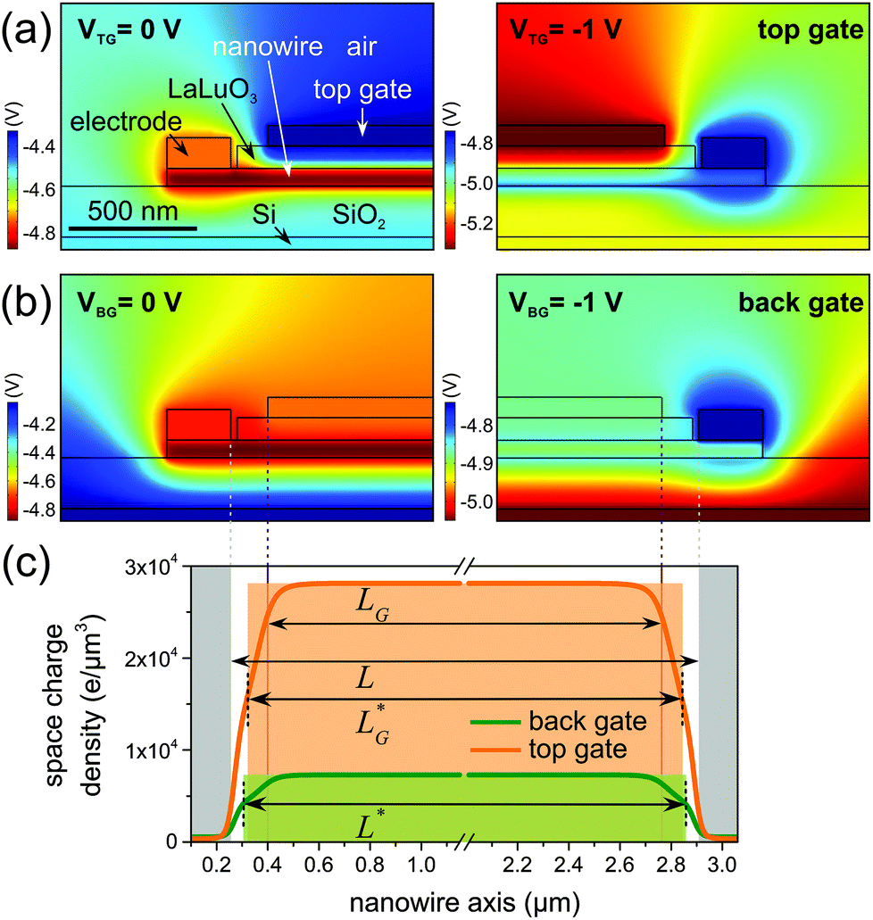 | ||
| Fig. 7 Potential distribution along the nanowire axis for device A with Ds = 3 × 1012 cm−2 eV−1 and for (a) top gate voltage VTG = 0 V (left), −1 V (right). The back gate is set to a floating potential. In (b) the potential distribution is depicted for back gate voltage VBG = 0 V (left), −1 V (right) and the top gate at a floating potential. Simulations are performed using the geometric dimensions of device A. (c) Distribution of space charge induced by ΔVG = −1 V at the center of the nanowire along the axis. | ||
Using the drift velocity  , with the bias voltage Vsd, the current can be expressed as a function of gate voltage, giving
 | (7) |
Taking into account the transconductance gm = dI/dVG, derived from the measurements in Fig. 6 and 8, the expression for the field-effect mobility is
 | (8) |
 | ||
| Fig. 8 Left: Transfer characteristics of (a) device D and (b) device E measured at room temperature using top and back gates. The bias voltage was set to 10 mV. Right: Electron concentration versus density of ionized dopants Nd for (a) device D and (b) device E, as calculated by means of eqn (6). In the insets, the capacitance is depicted as a function of Nd. | ||
In order to calculate the electron concentration from eqn (6), Vth is corrected for the work function difference between the gate and the InAs channel. The unused gate electrode is set to a floating potential in the measurements as well as in the numerical calculations. Nominally undoped nanowires can be utilized to determine the surface state density Ds, since the background doping level is a few orders of magnitude smaller than the overall charge concentration.14 In Fig. 6n is depicted as a function of Ds for devices A, B and C. At large Ds the two curves for the carrier density derived from top and back gate characteristics monotonously converge towards zero for either gate configuration at values of Ds beyond the realistic regime. This is obvious, since for large Ds the surface screens the nanowire bulk and renders the difference in electrostatic coupling between the two gates negligible. At intermediate values of Ds the curves intersect. The point of intersection is considered as the “sweet spot” where both types of measurement yield identical results. It is important to note that such a sweet spot has to exist for all devices, since the degree of freedom Ds is lifted by the two dissimilar and independent gates. The uniqueness of the sweet spot is due to the fact that it is possible to make both curves congruent via axis transformations. We find a sweet spot for the density of surface states of about 2.8 × 1012 cm−2 eV−1 for devices A and B and 3.1 × 1012 cm−2 eV−1 for device C. Thus, we arrive at a crossing of the electron concentrations at 5.1 × 1017 cm−3, 3.6 × 1017 cm−3 and 4.6 × 1017 cm−3 for device A, B and C, respectively. The field-effect mobilities for the three undoped devices are close to 1000 cm2 V−1 s−1 at the sweet spot of Ds, whereas the variation in the corresponding drift mobilities μd = 1/enρ is more pronounced. In the linear transport regime and for vanishing contact resistance, μd should equal μfe. However, in contrast to the threshold voltage, the transconductance used for calculating μfe and the resistivity which yields μd suffer from the uncertainty of the contact resistance. On average, the analysis of the undoped nanowires consistently points towards Ds ≈ 3 × 1012 cm−2 eV−1, which induces an average electron concentration of 4.4 × 1017 cm−3. The variations in mobility and resistivity among the undoped devices is a manifestation of their susceptibility to surface potential variations and surface scattering owing to the surface charge accumulation.
A key element of this analysis was the calculation of CBG and CTGvia finite element methods. However, commonly the capacitance of nanowire FETs is calculated utilizing an analytical cylinder-on-plane model:
 | (9) |
This formula holds for circular nanowires of diameter d located at a distance tox above a planar gate electrode, which is entirely surrounded by a gate dielectric of permittivity ε0εr. For hexagonal nanowires of outer diameter dNW an equivalent circular diameter  is used. However, it is well known,31 that this model has a number of flaws and is often not suitable to describe nanowire FETs properly. For instance, the nanowire is usually not entirely embedded in the gate dielectric. Furthermore, especially for short nanowires, the distortion of the electric field lines due to the presence of the metallic leads becomes important, resulting in “fringe capacitances”.32 Using eqn (9), the nanowire is treated as an equipotential. In reality however, there is a radial voltage drop inside the nanowire, which gives rise to an induced space charge. Above all, surface states are ubiquitous at semiconductor nanowire surfaces and also compete for the gate coupling. It turns out that the numerically calculated back gate capacitances are comparable in magnitude to the capacitances calculated from the cylinder-on-plane model using εr = 3.9 (see Table 1). However, this is a result of the large εr of LaLuO3, which compensates for corrections to eqn (9) related to surface capacitances and geometry. As discussed above, the surface states are critical and impose corrections of comparable magnitude as the corrections related to the semiconductivity.32 The large number of corrections to the common evaluation method presented in this work indicate that previous studies14 have overestimated n by more than 30%, when accounting for the hexagonal cross-section (there n ≈ 6 × 1017 cm−3). In contrast, μfe has been underestimated previously by about 30% (there μfe ≈ 700 cm2 V s−1).
Apart from eqn (9) the capacitance of nanowire FETs with Ω-shaped top gates is commonly described in literature by a model reflecting the wrap-around geometry of coaxial cables:
 | (10) |
However, eqn (10) is off by an even larger factor than the cylinder-on-plane model. The coaxial cable model overestimates CTG by a factor of almost 3, while the expression in eqn (9) can be corrected by a factor of ≈0.6 to account for CTG.11 The discrepancy between the current analytical models and our numerical results is large and the complex device geometries would require tremendous efforts to refine the analytical models. Using a simple capacitor model, which treats the accumulation layer (Cacc) and interface states (Cint) as parallel capacitors, the overall gate capacitance can be described by an effective capacitance correcting the mere geometric capacitance Cox connected in series:23
 | (11) |
Neglecting the curvature of the top gate, a factor of 0.6 corresponds to an accumulation layer thickness of 12 nm, i.e. the separation of the surface and the average charge location in the shallow surface quantum well. This result is in agreement with our self-consistent Schrödinger–Poisson solver calculations.
It was found that doping does not affect the crystal structure of the nanowires.14 Thus, it is a reasonable assumption that the surface state density Ds remains unchanged. Hence, we invoke the aforementioned result for Ds of the undoped devices of 3 × 1012 cm−2 eV−1 to calculate the capacitance of the doped devices to find the density of incorporated dopants. Since the ionized dopants supply the majority of free carriers for heavily doped nanowires, we choose to plot the electron concentration in Fig. 8versus Nd rather than versus Ds, as in Fig. 6. As depicted in Fig. 8, for the doped devices the curves for n using back and top gate cross for Nd in the range of 1019 cm−3, which is larger than the resulting sweet spot of n. Considering the uncertainty in extrapolating Vth from the gate traces of the doped devices, the agreement is reasonable, also with regard to the small effect variations of Nd have on the resulting n. It is well known that heavily doped semiconductors (Nd ∼ 1018 cm−3) exhibit conduction band tails due to the overlap with the donor levels leading to the fact that the donor electrons are delocalized.35,42 Hence, Nd corresponds to the actually ionized donor density. It is expected that the values for Nd and n agree quite well, since the carriers are predominantly supplied by the incorporated donor atoms in addition to a minor contribution from the surface states. We find that n is enhanced via doping by more than one order of magnitude to about 5 × 1018 cm−3. The average mobility however drops by a factor of 2. Both findings contrast previous results,14 where a more than 3-fold smaller n was found under identical doping conditions, when accounting for the hexagonal cross-section. The drift mobilities for devices D and E are 470 cm2 V−1 s−1 (see Table 1) and agree well with the field-effect mobilities (590 cm2 V−1 s−1 for device D and 450 cm2 V−1 s−1 for device E). Although the role of surface scattering is reduced for doped nanowires, since the electrons almost homogeneously populate the nanowire cross-section, the observed mobilities deteriorate due to an enhancement of scattering from ionized donors.
4 Conclusion
In conclusion, our work establishes how accurate electrostatic modeling of a nanowire FET in conjunction with dual-gate FET characterization can yield valuable information on the electronic properties of the nanowire surface and bulk. We have eliminated ambiguity in the interpretation of FET measurements by employing two gates with a pronounced difference in their capacitive coupling to the nanowire. The density of surface states is used as a free parameter to reconcile the derived transistor properties. We find a sweet spot of Ds = 3 × 1012 cm−2 eV−1, where both transfer characteristics yield identical results for the electron concentration and mobility. We demonstrate the striking impact of the presence of top gate high-k dielectrics on back gate capacitance. Our calculations confirm geometrical corrections to the conventional cylinder-on-plane model reported previously.31,32 Apart from the commonly neglected explicit device geometry and dielectric surrounding as well as the finite semiconductor capacitance, our simulations draw the attention towards the profound impact of the nanowire surface states on transistor functionality. Due to their capacitive effect surface states strongly mitigate the gate action. We find that about 25–30% of the charge is induced at the surface rather than in the electron accumulation layer and the nanowire bulk. Also Blömers et al.20 determined a surface charge density of a few 1012 cm−2 by comparing FET measurements with room temperature Hall measurements on single nanowires. Invoking a reasonable energy distribution width on the order of 100 meV, this corresponds to Ds ≈ 1013 cm−2 eV−1, which is in good agreement with the present analysis of the dual-gated nanowire FET. Similar results were found by C–V measurements on InAs nanowire arrays by Astromskas et al.26 where a surface charge density of 5 × 1012 cm−2 was calculated. Halpern et al.30 have utilized Kelvin probe force microscopy on an individual InAs nanowire and measured the energy distribution of Ds with a maximum of 1013 cm−2 eV−1. Our results are also in agreement with investigations on InAs layers by Noguchi et al.17 who found surface charge densities that translate to Ds on the order of 1012 cm−2 eV−1.The dramatic impact of surface states on electronic transport in InAs nanowires has been under debate previously.43 The conflicting results which advocate for44 and against45 the existence of surface electron gases at InAs nanowire surfaces might be explained by the shallowness of the triangular quantum well forming the 2DEG. The value for Ds we find only gives rise to a weak Fermi level pinning (cf.Fig. 3) just 60 meV above the conduction band edge. For all gate configurations depicted in Fig. 5b and c the corrections to the capacitances in the metallic limit (i.e. reflecting merely the dielectric surrounding31) can be accounted for by a factor of 0.6. This comprises corrections due to the addition of surface states and voltage drops inside the undoped nanowire. For the most common nanowire-FET device with SiO2-based back gate (undoped and hexagonal nanowires) an effective permittivity of  can be employed for the analytical evaluation using eqn (9). In the presence of the LaLuO3 top gate dielectric (conf.Fig. 5c) the back gate
  is enhanced from εr = 3.9 to about 4.4, while the top gate
  is reduced from εr = 26.9 to about 15.2. A limitation of our model is that the consideration of trap states inside the SiO2 or the LaLuO3 might lead to further corrections. However, it is expected that trap states are not as decisive for transistor functionality as the nanowire/dielectric interface states.28 More critical might be the assumption of a fixed value of Ds for all facets, albeit detailed assumptions on the exact distribution would be unsubstantiated. For very narrow nanowires also quantum confinement effects have to be taken into account.
The presented methodology offers a beneficial tool to accurately determine nanowire transport properties and demands substantial corrections to carrier concentrations and mobilities commonly derived from analytical models.
Acknowledgements
We are grateful to St. Trellenkamp for performing electron beam lithography. This work has been supported by the German Research Foundation (DFG) via FOR 912.References
- C. Thelander, P. Agarwal, S. Brongersma, J. Eymery, L. Feiner, A. Forchel, M. Scheffler, W. Riess, B. Ohlsson, U. Gösele and L. Samuelson, Mater. Today, 2006, 9, 28–35 CrossRef CAS
.
- T. Bryllert, L.-E. Wernersson, L. Froberg and L. Samuelson, IEEE Electron Device Lett., 2006, 27, 323–325 CrossRef CAS
- H. Yan, H. S. Choe, S. Nam, Y. Hu, S. Das, J. F. Klemic, J. C. Ellenbogen and C. M. Lieber, Nature, 2011, 470, 240–244 CrossRef CAS PubMed
- J. Xiang, W. Lu, Y. Hu, Y. Wu, H. Yan and C. M. Lieber, Nature, 2011, 441, 489–493 CrossRef PubMed
- J. Du, D. Liang, H. Tang and X. P. Gao, Nano Lett., 2009, 9, 4348–4351 CrossRef CAS PubMed
- G. Zheng, X. P. A. Gao and C. M. Lieber, Nano Lett., 2010, 10, 3179–3183 CrossRef CAS PubMed
- W. Lu, J. Xiang, B. P. Timko, Y. Wu and C. M. Lieber, Proc. Natl. Acad. Sci. U. S. A., 2005, 102, 10046–10051 CrossRef CAS PubMed
- V. Mourik, K. Zuo, S. M. Frolov, S. R. Plissard, E. P. A. M. Bakkers and L. P. Kouwenhoven, Science, 2012, 336, 1003–1007 CrossRef CAS PubMed
- I. van Weperen, S. R. Plissard, E. P. A. M. Bakkers, S. M. Frolov and L. P. Kouwenhoven, Nano Lett., 2013, 13, 387–391 CrossRef CAS PubMed
- S. A. Dayeh, D. P. R. Aplin, X. Zhou, P. K. L. Yu, E. T. Yu and D. Wang, Small, 2007, 3, 326–332 CrossRef CAS PubMed
- C. Volk, J. Schubert, M. Schnee, K. Weis, M. Akabori, K. Sladek, H. Hardtdegen and Th. Schäpers, Semicond. Sci. Technol., 2010, 25, 085001 CrossRef
- C. Fasth, A. Fuhrer, M. T. Björk and L. Samuelson, Nano Lett., 2005, 5, 1487–1490 CrossRef CAS PubMed
- P. D. Nissen, T. S. Jespersen, K. Grove-Rasmussen, A. Márton, S. Upadhyay, M. H. Madsen, S. Csonka and J. Nygård, J. Appl. Phys., 2012, 112, 084323 CrossRef
- S. Wirths, K. Weis, A. Winden, K. Sladek, C. Volk, S. Alagha, T. E. Weirich, M. von der Ahe, H. Hardtdegen, H. Lüth, N. Demarina, D. Grützmacher and Th. Schäpers, J. Appl. Phys., 2011, 110, 053709 CrossRef
- O. Karlström, A. Wacker, K. Nilsson, G. Astromskas, S. Roddaro, L. Samuelson and L.-E. Wernersson, Nanotechnology, 2008, 19, 435201 CrossRef PubMed
- K. Storm, G. Nylund, L. Samuelson and A. P. Micolich, Nano Lett., 2012, 12, 1–6 CrossRef CAS PubMed
- M. Noguchi, K. Hirakawa and T. Ikoma, Phys. Rev. Lett., 1991, 66, 2243–2246 CrossRef CAS PubMed
- B. Z. Nosho, W. H. Weinberg, W. Barvosa-Carter, B. R. Bennett, B. V. Shanabrook and L. J. Whitman, Appl. Phys. Lett., 1999, 74, 1704–1706 CrossRef CAS
- J. Moers, S. Trellenkamp, D. Grützmacher, A. Offenhäusser and B. Rienks, Microelectron. Eng., 2012, 97, 68–71 CrossRef CAS
- Ch. Blömers, T. Grap, M. I. Lepsa, J. Moers, St. Trellenkamp, D. Grützmacher, H. Lüth and Th. Schäpers, Appl. Phys. Lett., 2012, 101, 152106 CrossRef
- K. Storm, F. Halvardsson, M. Heurlin, D. Lindgren, A. Gustafsson, P. M. Wu, B. Monemar and L. Samuelson, Nat. Nanotechnol., 2012, 7, 718–722 CrossRef CAS PubMed
- E. Lind, A. I. Persson, L. Samuelson and L.-E. Wernersson, Nano Lett., 2006, 6, 1842–1846 CrossRef CAS PubMed
- S. A. Dayeh, C. Soci, P. K. L. Yu, E. T. Yu and D. Wang, J. Vac. Sci. Technol., B, 2007, 25, 1432–1436 Search PubMed
-
N. V. Demarina, M. I. Lepsa and D. Grützmacher, Future Trends in Microelectronics: Frontiers and Innovations, Wiley-IEEE Press, 2013, pp. 351–358 Search PubMed
- S. Roddaro, K. Nilsson, G. Astromskas, L. Samuelson, L.-E. Wernersson, O. Karlström and A. Wacker, Appl. Phys. Lett., 2008, 92, 253509 CrossRef
- G. Astromskas, K. Storm, O. Karlström, P. Caroff, M. Borgström and L.-E. Wernersson, J. Appl. Phys., 2010, 108, 054306 CrossRef
- R. Tu, L. Zhang, Y. Nishi and H. Dai, Nano Lett., 2007, 7, 1561–1565 CrossRef CAS PubMed
- A. C. Ford, J. C. Ho, Y.-L. Chueh, Y.-C. Tseng, Z. Fan, J. Guo, J. Bokor and A. Javey, Nano Lett., 2009, 9, 360–365 CrossRef CAS PubMed
- N. Clément, K. Nishiguchi, A. Fujiwara and D. Vuillaume, IEEE Trans. Nanotechnol., 2011, 10, 1172–1179 CrossRef
- E. Halpern, G. Elias, A. V. Kretinin, H. Shtrikman and Y. Rosenwaks, Appl. Phys. Lett., 2012, 100, 262105 CrossRef
- O. Wunnicke, Appl. Phys. Lett., 2006, 89, 083102 CrossRef
- D. R. Khanal and J. Wu, Nano Lett., 2007, 7, 2778–2783 CrossRef CAS PubMed
- M. Akabori, K. Sladek, H. Hardtdegen, Th. Schäpers and D. Grützmacher, J. Cryst. Growth, 2009, 311, 3813–3816 CrossRef CAS
- E. D. Özben, J. M. J. Lopes, A. Nichau, M. Schnee, S. Lenk, A. Besmehn, K. Bourdelle, Q. Zhao, J. Schubert and S. Mantl, IEEE Electron Device Lett., 2011, 32, 15–17 CrossRef
-
H. Ibach and H. Lüth, Solid-State Physics, Springer, Berlin Heidelberg, 2009 Search PubMed
- E. O. Kane, J. Phys. Chem. Solids, 1957, 1, 249–261 CrossRef
- M. Cardona, J. Phys. Chem. Solids, 1963, 24, 1543–1555 CrossRef CAS
- I. Vurgaftman, J. R. Meyer and L. R. Ram-Mohan, J. Appl. Phys., 2001, 89, 5815–5875 CrossRef CAS
- C. Affentauschegg and H. H. Wieder, Semicond. Sci. Technol., 2001, 16, 708 CrossRef CAS
- K. Smit, L. Koenders and W. Mönch, J. Vac. Sci. Technol., B, 1989, 7, 888–893 Search PubMed
- J. Smoliner and C. Eder, Phys. Rev. B: Condens. Matter, 1998, 57, 9856–9860 CrossRef CAS
- P. Van Mieghem, Rev. Mod. Phys., 1992, 64, 755–793 CrossRef CAS
- Ch. Blömers, M. I. Lepsa, M. Luysberg, D. Grützmacher, H. Lüth and Th. Schäpers, Nano Lett., 2011, 11, 3550–3556 CrossRef PubMed
- M. Scheffler, S. Nadj-Perge, L. P. Kouwenhoven, M. T. Borgström and E. P. A. M. Bakkers, J. Appl. Phys., 2009, 106, 124303 CrossRef
- T. S. Jespersen, J. R. Hauptmann, C. B. Sørensen and J. Nygård, Phys. Rev. B: Condens. Matter, 2015, 91, 041302 CrossRef
| This journal is © The Royal Society of Chemistry 2015 |